EP0138329A2 - Einrichtung und Verfahren zur Steuerung einer Anzeigeeinrichtung mit Speichereigenschaft - Google Patents
Einrichtung und Verfahren zur Steuerung einer Anzeigeeinrichtung mit Speichereigenschaft Download PDFInfo
- Publication number
- EP0138329A2 EP0138329A2 EP84305588A EP84305588A EP0138329A2 EP 0138329 A2 EP0138329 A2 EP 0138329A2 EP 84305588 A EP84305588 A EP 84305588A EP 84305588 A EP84305588 A EP 84305588A EP 0138329 A2 EP0138329 A2 EP 0138329A2
- Authority
- EP
- European Patent Office
- Prior art keywords
- scan
- sustainer
- cells
- period
- display
- Prior art date
- Legal status (The legal status is an assumption and is not a legal conclusion. Google has not performed a legal analysis and makes no representation as to the accuracy of the status listed.)
- Granted
Links
- 238000000034 method Methods 0.000 title description 7
- 230000006870 function Effects 0.000 claims description 3
- 230000001360 synchronised effect Effects 0.000 claims 2
- 239000011159 matrix material Substances 0.000 abstract description 3
- 230000000694 effects Effects 0.000 description 5
- 229910052751 metal Inorganic materials 0.000 description 5
- 239000002184 metal Substances 0.000 description 5
- 239000002245 particle Substances 0.000 description 5
- 238000010304 firing Methods 0.000 description 3
- 239000011521 glass Substances 0.000 description 3
- 230000037452 priming Effects 0.000 description 3
- 239000011248 coating agent Substances 0.000 description 2
- 238000000576 coating method Methods 0.000 description 2
- 239000004020 conductor Substances 0.000 description 2
- 238000010276 construction Methods 0.000 description 2
- 239000011810 insulating material Substances 0.000 description 2
- 230000008569 process Effects 0.000 description 2
- 230000002459 sustained effect Effects 0.000 description 2
- 238000005513 bias potential Methods 0.000 description 1
- 230000008878 coupling Effects 0.000 description 1
- 238000010168 coupling process Methods 0.000 description 1
- 238000005859 coupling reaction Methods 0.000 description 1
- 230000009977 dual effect Effects 0.000 description 1
- 230000008030 elimination Effects 0.000 description 1
- 238000003379 elimination reaction Methods 0.000 description 1
- 230000008020 evaporation Effects 0.000 description 1
- 238000001704 evaporation Methods 0.000 description 1
- 230000006872 improvement Effects 0.000 description 1
- 230000002452 interceptive effect Effects 0.000 description 1
- CPLXHLVBOLITMK-UHFFFAOYSA-N magnesium oxide Inorganic materials [Mg]=O CPLXHLVBOLITMK-UHFFFAOYSA-N 0.000 description 1
- 239000000395 magnesium oxide Substances 0.000 description 1
- AXZKOIWUVFPNLO-UHFFFAOYSA-N magnesium;oxygen(2-) Chemical compound [O-2].[Mg+2] AXZKOIWUVFPNLO-UHFFFAOYSA-N 0.000 description 1
- 239000000463 material Substances 0.000 description 1
- 230000007246 mechanism Effects 0.000 description 1
- 239000000203 mixture Substances 0.000 description 1
- 230000004048 modification Effects 0.000 description 1
- 238000012986 modification Methods 0.000 description 1
- 229910052754 neon Inorganic materials 0.000 description 1
- GKAOGPIIYCISHV-UHFFFAOYSA-N neon atom Chemical compound [Ne] GKAOGPIIYCISHV-UHFFFAOYSA-N 0.000 description 1
- 229910052709 silver Inorganic materials 0.000 description 1
- 239000004332 silver Substances 0.000 description 1
- 125000006850 spacer group Chemical group 0.000 description 1
- 238000004544 sputter deposition Methods 0.000 description 1
- 230000001629 suppression Effects 0.000 description 1
- ZCUFMDLYAMJYST-UHFFFAOYSA-N thorium dioxide Chemical compound O=[Th]=O ZCUFMDLYAMJYST-UHFFFAOYSA-N 0.000 description 1
- 229910003452 thorium oxide Inorganic materials 0.000 description 1
- 230000007704 transition Effects 0.000 description 1
- 229910052724 xenon Inorganic materials 0.000 description 1
- FHNFHKCVQCLJFQ-UHFFFAOYSA-N xenon atom Chemical compound [Xe] FHNFHKCVQCLJFQ-UHFFFAOYSA-N 0.000 description 1
Images


Classifications
-
- G—PHYSICS
- G09—EDUCATION; CRYPTOGRAPHY; DISPLAY; ADVERTISING; SEALS
- G09G—ARRANGEMENTS OR CIRCUITS FOR CONTROL OF INDICATING DEVICES USING STATIC MEANS TO PRESENT VARIABLE INFORMATION
- G09G3/00—Control arrangements or circuits, of interest only in connection with visual indicators other than cathode-ray tubes
- G09G3/20—Control arrangements or circuits, of interest only in connection with visual indicators other than cathode-ray tubes for presentation of an assembly of a number of characters, e.g. a page, by composing the assembly by combination of individual elements arranged in a matrix no fixed position being assigned to or needed to be assigned to the individual characters or partial characters
- G09G3/22—Control arrangements or circuits, of interest only in connection with visual indicators other than cathode-ray tubes for presentation of an assembly of a number of characters, e.g. a page, by composing the assembly by combination of individual elements arranged in a matrix no fixed position being assigned to or needed to be assigned to the individual characters or partial characters using controlled light sources
- G09G3/28—Control arrangements or circuits, of interest only in connection with visual indicators other than cathode-ray tubes for presentation of an assembly of a number of characters, e.g. a page, by composing the assembly by combination of individual elements arranged in a matrix no fixed position being assigned to or needed to be assigned to the individual characters or partial characters using controlled light sources using luminous gas-discharge panels, e.g. plasma panels
- G09G3/2813—Control arrangements or circuits, of interest only in connection with visual indicators other than cathode-ray tubes for presentation of an assembly of a number of characters, e.g. a page, by composing the assembly by combination of individual elements arranged in a matrix no fixed position being assigned to or needed to be assigned to the individual characters or partial characters using controlled light sources using luminous gas-discharge panels, e.g. plasma panels using alternating current [AC] - direct current [DC] hybrid-type panels
Definitions
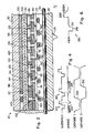
- a plurality of scan cathode electrodes 60 are seated on the top surface of the base plate or in shallow grooves 70 therein.
- the grooves 70 and scan cathodes 60 are disposed transverse to the grooves 40 and scan anodes 50, and each crossing of a scan cathode 60 and scan anode 50 defines a scanning cell 72 (Fig. 2).
- the anodes 50 and cathodes 60 form a matrix of scanning cells which are arrayed in rows and columns. More specifically, the cathode portions 61, the underlying portions of anodes 50, and the intermediate gas volumes define the scanning cells.
- a reset cathode strip 62 is disposed on the base plate or in a groove 64 therein adjacent to the first scan cathode 60A, so that, when it is energized, it provides excited particles for cathode 60A at the beginning of a scanning cycle to be described.
- the reset cathode crosses each scan anode 50, a reset cell is formed, and the crossing of all of the scan anodes by the reset cathode provides a column of reset cells.
- These reset cells are turned on or energized at the beginning of each scanning cycle, and they expedite the turn-on of the first column of scanning cells associated with cathode 60A.
- the portions of the panel described up to this point comprise the base plate assembly. This is the D.C. portion and the scanning and addressing portion of the panel 10 in which the electrodes are in contact with the gas in the panel.
- the slot 142 overlies and is aligned with the column of holes 150, and both lie beneath and are aligned with the A.C. electrode 140 so that, in effect, the electrode 140, slot 142 and holes 150 form a sandwich.
- the slot 142 in the plate 86 is narrower than the opaque A.C. electrode 140 so that a viewer, looking through face plate 30, cannot see any glow which is present in slot 142 and holes 150.
- Electrode 140 operates with plate 80 to produce glow discharge between them and produce excited particles in slot 142 and holes 150. These excited particles are available to the reset cathode 62 and assist the firing of the column of reset cells.
- the circuit includes a keep-alive driver 170, which provides an A.C. signal, suitably coupled to keep-alive electrode 140.
- the system also includes module 172 which comprises a series of serially energizable drivers for providing a negative reset pulse for reset cathode 62 on lead 173 and a series of negative scan cathode pulses for cathodes 60 on leads 174.
- the scan cathodes 60 are connected in groups or phases, with each group including any suitable number of cathodes such as three or four or six, or more, as desired.
- a D.C. power source 185 is coupled through a resistive path to each of the scan anodes 50.
- separate data drivers 183 each of which represents a source of write pulses and erase pulses, are coupled, one to each scan/address anode 50.
- a source 187 of D.C. bias potential is coupled to priming plate 80, and a source 200 of A.C. sustainer signals, is connected to the transparent conductive layer 100.
- the erasing operation is generally similar to the writing operation described above.
- the selected display cell is operated upon while its underlying scan cell is being scanned, but the erase signal is applied in synchronism with, but following, the negative sustainer pulse.
- the associated scan cell is again turned off momentarily, and then it is turned back on, to avoid interfering with the normal column-by-column scan of the scan cells. While it is off, the decaying discharge around electrode portion 61 again produces electron flow to electrode 80, and through the aperture in that electrode into the display cell.
- transistor 260 performs a dual function in switching the sustaining signal either from 200 volts to the reference level of 80 volts or from zero volts to the reference level of 80 volts.
- the positive or negative transition of the switching operation of transistor 260 is determined by the sustain output voltage level prior to switching and the resultant path through the diode bridge 274. If the sustain output level is at 200 volts, the turn-on of transistor 260 will cause the sustain output to switch in a negative direction to 80 volts due to the low impedance path to the 80 volt bus 288 by way of resistors 279, diode 284, transistor 260, and diode 286. Diodes 285 and 287 are open circuited.
- the turn-on of the transistor 260 will cause the sustain level to switch in a positive direction along a low impedance path to the 80 volt bus 388 by way of resistor 279, diode 287, transistor 260, and diode 285, with diodes 284 and 286 being open circuited.
- the desired average brightness of the viewed panel can be achieved.
- a wide range of panel brightnesses is possible.
- a period of brightness compensation (like period B) may be inserted before write period C or after write period C, or having a small portion before and after write period C.
- the particular routine can be readily determined by those skilled in the art.
Landscapes
- Engineering & Computer Science (AREA)
- Physics & Mathematics (AREA)
- Plasma & Fusion (AREA)
- Computer Hardware Design (AREA)
- General Physics & Mathematics (AREA)
- Theoretical Computer Science (AREA)
- Control Of Indicators Other Than Cathode Ray Tubes (AREA)
Applications Claiming Priority (2)
| Application Number | Priority Date | Filing Date | Title |
|---|---|---|---|
| US06/525,282 US4595919A (en) | 1983-08-22 | 1983-08-22 | System and method for operating a display panel having memory |
| US525282 | 1983-08-22 |
Publications (3)
| Publication Number | Publication Date |
|---|---|
| EP0138329A2 true EP0138329A2 (de) | 1985-04-24 |
| EP0138329A3 EP0138329A3 (en) | 1987-08-26 |
| EP0138329B1 EP0138329B1 (de) | 1990-09-19 |
Family
ID=24092621
Family Applications (1)
| Application Number | Title | Priority Date | Filing Date |
|---|---|---|---|
| EP84305588A Expired - Lifetime EP0138329B1 (de) | 1983-08-22 | 1984-08-17 | Einrichtung und Verfahren zur Steuerung einer Anzeigeeinrichtung mit Speichereigenschaft |
Country Status (5)
| Country | Link |
|---|---|
| US (1) | US4595919A (de) |
| EP (1) | EP0138329B1 (de) |
| JP (1) | JPS6095494A (de) |
| CA (1) | CA1233921A (de) |
| DE (1) | DE3483233D1 (de) |
Cited By (1)
| Publication number | Priority date | Publication date | Assignee | Title |
|---|---|---|---|---|
| KR101218583B1 (ko) * | 2007-06-18 | 2013-01-22 | 콸콤 인코포레이티드 | 핸드오프에서 pdcp 재정렬을 위한 방법 및 장치 |
Families Citing this family (12)
| Publication number | Priority date | Publication date | Assignee | Title |
|---|---|---|---|---|
| EP0193728B1 (de) * | 1985-03-08 | 1992-08-19 | Ascii Corporation | Anzeigesteuersystem |
| JPS62171385A (ja) * | 1986-01-24 | 1987-07-28 | Mitsubishi Electric Corp | 中間調表示方式 |
| EP0249954B1 (de) * | 1986-06-17 | 1992-12-02 | Fujitsu Limited | Ansteuerung für eine Anzeigevorrichtung in Matrix-Form |
| JPH0634148B2 (ja) * | 1986-07-22 | 1994-05-02 | 日本電気株式会社 | プラズマデイスプレイ装置 |
| US5077553A (en) * | 1988-01-19 | 1991-12-31 | Tektronix, Inc. | Apparatus for and methods of addressing data storage elements |
| US5247288A (en) * | 1989-11-06 | 1993-09-21 | Board Of Trustees Of University Of Illinois | High speed addressing method and apparatus for independent sustain and address plasma display panel |
| US5311204A (en) * | 1991-08-28 | 1994-05-10 | Tektronix, Inc. | Offset electrodes |
| JPH06282242A (ja) * | 1993-03-25 | 1994-10-07 | Pioneer Electron Corp | ガス放電パネルの駆動方法 |
| US5949197A (en) * | 1997-06-30 | 1999-09-07 | Everbrite, Inc. | Apparatus and method for dimming a gas discharge lamp |
| JP2003140605A (ja) * | 2001-08-24 | 2003-05-16 | Sony Corp | プラズマ表示装置及びその駆動方法 |
| KR100515299B1 (ko) | 2003-04-30 | 2005-09-15 | 삼성에스디아이 주식회사 | 화상 표시 장치와 그 표시 패널 및 구동 방법 |
| US11538435B2 (en) * | 2020-12-08 | 2022-12-27 | Sharp Kabushiki Kaisha | Dimming panel and liquid crystal display device |
Family Cites Families (9)
| Publication number | Priority date | Publication date | Assignee | Title |
|---|---|---|---|---|
| US3778673A (en) * | 1971-06-21 | 1973-12-11 | Burroughs Corp | Low power display driver having brightness control |
| US3919591A (en) * | 1973-06-29 | 1975-11-11 | Ibm | Gas panel with improved write-erase and sustain circuits and operations |
| US4067047A (en) * | 1976-03-29 | 1978-01-03 | Owens-Illinois, Inc. | Circuit and method for generating gray scale in gaseous discharge panels |
| US4386348A (en) * | 1979-06-22 | 1983-05-31 | Burroughs Corporation | Display panel having memory |
| US4385293A (en) * | 1979-12-10 | 1983-05-24 | United Technologies Corporation | Gray shade operation of a large AC plasma display panel |
| US4329616A (en) * | 1979-12-31 | 1982-05-11 | Burroughs Corporation | Keep-alive electrode arrangement for display panel having memory |
| US4315259A (en) * | 1980-10-24 | 1982-02-09 | Burroughs Corporation | System for operating a display panel having memory |
| US4373157A (en) * | 1981-04-29 | 1983-02-08 | Burroughs Corporation | System for operating a display panel |
| US4414544A (en) * | 1981-06-12 | 1983-11-08 | Interstate Electronics Corp. | Constant data rate brightness control for an AC plasma panel |
-
1983
- 1983-08-22 US US06/525,282 patent/US4595919A/en not_active Expired - Lifetime
-
1984
- 1984-08-15 CA CA000461057A patent/CA1233921A/en not_active Expired
- 1984-08-17 EP EP84305588A patent/EP0138329B1/de not_active Expired - Lifetime
- 1984-08-17 DE DE8484305588T patent/DE3483233D1/de not_active Expired - Lifetime
- 1984-08-21 JP JP59174864A patent/JPS6095494A/ja active Pending
Cited By (1)
| Publication number | Priority date | Publication date | Assignee | Title |
|---|---|---|---|---|
| KR101218583B1 (ko) * | 2007-06-18 | 2013-01-22 | 콸콤 인코포레이티드 | 핸드오프에서 pdcp 재정렬을 위한 방법 및 장치 |
Also Published As
| Publication number | Publication date |
|---|---|
| DE3483233D1 (de) | 1990-10-25 |
| EP0138329B1 (de) | 1990-09-19 |
| CA1233921A (en) | 1988-03-08 |
| EP0138329A3 (en) | 1987-08-26 |
| US4595919A (en) | 1986-06-17 |
| JPS6095494A (ja) | 1985-05-28 |
Similar Documents
| Publication | Publication Date | Title |
|---|---|---|
| US4554537A (en) | Gas plasma display | |
| US3769543A (en) | Low voltage gas discharge display | |
| US4595919A (en) | System and method for operating a display panel having memory | |
| US4315259A (en) | System for operating a display panel having memory | |
| US4253044A (en) | Gas discharge display panel, display apparatus comprising the panel and method of operating the display apparatus | |
| JPS63309994A (ja) | 1画素につき4つの電極を有するプラズマディスプレイパネルとその制御方法 | |
| US4613854A (en) | System for operating a dot matrix display panel to prevent crosstalk | |
| EP0023082B1 (de) | Anzeigevorrichtung und Verfahren in ihrem Betrieb | |
| US4373157A (en) | System for operating a display panel | |
| US4532505A (en) | Gas-filled dot matrix display panel | |
| Weston | Plasma panel displays | |
| WO1983003157A1 (en) | Plasma display panel with scan-only columns | |
| EP0138330B1 (de) | Verfahren und Einrichtung zur Steuerung einer Anzeigeeinrichtung mit Speichereigenschaft | |
| EP0122072B1 (de) | Gasgefüllte Punkt-Matrix-Anzeigeeinheit und Betriebssystem | |
| US4031429A (en) | Information display and method of operating with storage | |
| US3767968A (en) | Panel-type display device having display cells and auxiliary cells for operating them | |
| US4099096A (en) | Information display and method of operating with storage | |
| US4010395A (en) | Gas discharge display panel with cell-firing means having glow spreading electrode | |
| US4035689A (en) | Panel-type display device | |
| US3781587A (en) | Gas discharge display apparatus | |
| US4147959A (en) | Display section for multilayer gas-discharge display panel | |
| US4156164A (en) | Display device using hot cathode gas discharge | |
| US4047169A (en) | Display panel having improved arrangement of reset cells for facilitating scanning of the panel | |
| US4065699A (en) | Cathode assembly for two-dimensional scanned gas discharge display panel | |
| US4107576A (en) | Panel-type display device |
Legal Events
| Date | Code | Title | Description |
|---|---|---|---|
| PUAI | Public reference made under article 153(3) epc to a published international application that has entered the european phase |
Free format text: ORIGINAL CODE: 0009012 |
|
| 17P | Request for examination filed |
Effective date: 19840901 |
|
| AK | Designated contracting states |
Designated state(s): BE DE FR GB IT NL SE |
|
| RAP1 | Party data changed (applicant data changed or rights of an application transferred) |
Owner name: BURROUGHS CORPORATION (A DELAWARE CORPORATION) |
|
| RAP1 | Party data changed (applicant data changed or rights of an application transferred) |
Owner name: UNISYS CORPORATION |
|
| PUAL | Search report despatched |
Free format text: ORIGINAL CODE: 0009013 |
|
| AK | Designated contracting states |
Kind code of ref document: A3 Designated state(s): BE DE FR GB IT NL SE |
|
| 17Q | First examination report despatched |
Effective date: 19890830 |
|
| GRAA | (expected) grant |
Free format text: ORIGINAL CODE: 0009210 |
|
| AK | Designated contracting states |
Kind code of ref document: B1 Designated state(s): BE DE FR GB IT NL SE |
|
| PG25 | Lapsed in a contracting state [announced via postgrant information from national office to epo] |
Ref country code: SE Effective date: 19900919 Ref country code: NL Effective date: 19900919 Ref country code: IT Free format text: LAPSE BECAUSE OF FAILURE TO SUBMIT A TRANSLATION OF THE DESCRIPTION OR TO PAY THE FEE WITHIN THE PRESCRIBED TIME-LIMIT;WARNING: LAPSES OF ITALIAN PATENTS WITH EFFECTIVE DATE BEFORE 2007 MAY HAVE OCCURRED AT ANY TIME BEFORE 2007. THE CORRECT EFFECTIVE DATE MAY BE DIFFERENT FROM THE ONE RECORDED. Effective date: 19900919 Ref country code: BE Effective date: 19900919 |
|
| ET | Fr: translation filed | ||
| REF | Corresponds to: |
Ref document number: 3483233 Country of ref document: DE Date of ref document: 19901025 |
|
| NLV1 | Nl: lapsed or annulled due to failure to fulfill the requirements of art. 29p and 29m of the patents act | ||
| PLBE | No opposition filed within time limit |
Free format text: ORIGINAL CODE: 0009261 |
|
| STAA | Information on the status of an ep patent application or granted ep patent |
Free format text: STATUS: NO OPPOSITION FILED WITHIN TIME LIMIT |
|
| 26N | No opposition filed | ||
| PGFP | Annual fee paid to national office [announced via postgrant information from national office to epo] |
Ref country code: GB Payment date: 19930708 Year of fee payment: 10 |
|
| PGFP | Annual fee paid to national office [announced via postgrant information from national office to epo] |
Ref country code: FR Payment date: 19930808 Year of fee payment: 10 |
|
| PGFP | Annual fee paid to national office [announced via postgrant information from national office to epo] |
Ref country code: DE Payment date: 19930825 Year of fee payment: 10 |
|
| PG25 | Lapsed in a contracting state [announced via postgrant information from national office to epo] |
Ref country code: GB Effective date: 19940817 |
|
| GBPC | Gb: european patent ceased through non-payment of renewal fee |
Effective date: 19940817 |
|
| PG25 | Lapsed in a contracting state [announced via postgrant information from national office to epo] |
Ref country code: FR Effective date: 19950428 |
|
| PG25 | Lapsed in a contracting state [announced via postgrant information from national office to epo] |
Ref country code: DE Effective date: 19950503 |
|
| REG | Reference to a national code |
Ref country code: FR Ref legal event code: ST |