EP0138440A2 - Fokussierungsvorrichtung für eine Röntgenstrahlungspunktquelle - Google Patents
Fokussierungsvorrichtung für eine Röntgenstrahlungspunktquelle Download PDFInfo
- Publication number
- EP0138440A2 EP0138440A2 EP84306510A EP84306510A EP0138440A2 EP 0138440 A2 EP0138440 A2 EP 0138440A2 EP 84306510 A EP84306510 A EP 84306510A EP 84306510 A EP84306510 A EP 84306510A EP 0138440 A2 EP0138440 A2 EP 0138440A2
- Authority
- EP
- European Patent Office
- Prior art keywords
- focusing
- layer pairs
- ray
- forming
- section
- Prior art date
- Legal status (The legal status is an assumption and is not a legal conclusion. Google has not performed a legal analysis and makes no representation as to the accuracy of the status listed.)
- Withdrawn
Links
Images


Classifications
-
- G—PHYSICS
- G21—NUCLEAR PHYSICS; NUCLEAR ENGINEERING
- G21K—HANDLING OF PARTICLES OR IONISING RADIATION NOT OTHERWISE PROVIDED FOR; IRRADIATION DEVICES; GAMMA RAY OR X-RAY MICROSCOPES
- G21K1/00—Arrangements for handling particles or ionising radiation, e.g. focusing or moderating
- G21K1/06—Arrangements for handling particles or ionising radiation, e.g. focusing or moderating using diffraction, refraction or reflection, e.g. monochromators
- G21K1/062—Devices having a multilayer structure
-
- B—PERFORMING OPERATIONS; TRANSPORTING
- B82—NANOTECHNOLOGY
- B82Y—SPECIFIC USES OR APPLICATIONS OF NANOSTRUCTURES; MEASUREMENT OR ANALYSIS OF NANOSTRUCTURES; MANUFACTURE OR TREATMENT OF NANOSTRUCTURES
- B82Y10/00—Nanotechnology for information processing, storage or transmission, e.g. quantum computing or single electron logic
-
- G—PHYSICS
- G21—NUCLEAR PHYSICS; NUCLEAR ENGINEERING
- G21K—HANDLING OF PARTICLES OR IONISING RADIATION NOT OTHERWISE PROVIDED FOR; IRRADIATION DEVICES; GAMMA RAY OR X-RAY MICROSCOPES
- G21K2201/00—Arrangements for handling radiation or particles
- G21K2201/06—Arrangements for handling radiation or particles using diffractive, refractive or reflecting elements
- G21K2201/061—Arrangements for handling radiation or particles using diffractive, refractive or reflecting elements characterised by a multilayer structure
-
- G—PHYSICS
- G21—NUCLEAR PHYSICS; NUCLEAR ENGINEERING
- G21K—HANDLING OF PARTICLES OR IONISING RADIATION NOT OTHERWISE PROVIDED FOR; IRRADIATION DEVICES; GAMMA RAY OR X-RAY MICROSCOPES
- G21K2201/00—Arrangements for handling radiation or particles
- G21K2201/06—Arrangements for handling radiation or particles using diffractive, refractive or reflecting elements
- G21K2201/064—Arrangements for handling radiation or particles using diffractive, refractive or reflecting elements having a curved surface
Definitions
- This invention relates to an improved point source X-ray focusing device.
- the device utilizes synthetic layered structures which are free from the constraints of crystalline symmetries.
- the layers are formed on a focusing element surface which is selected to collect, reflect and focus the maximum X-ray flux from the point source to a focus point for a particular wavelength of interest.
- X-ray dispersive structures are formed from crystalline structures such as LiF, metal acid phthalates (map), pyrolytic graphite and Langmuir-Blodgett (LB) films. These materials have very restrictive lattice spacing constraints.
- the LB and map devices have severe environmental limitations and must be operated near room temperature in a dry environment. LB devices are not appropriate for very high vacuum applications since under certain conditions they can evolve contaminants. They are also inappropriate for high incident beam energy applications since they can decompose. They have poor mechanical integrity, such as scratch resistance, mechanical breaking strength and resistance to abrasion. Further, all of the prior structures have lower reflectivities than desired.
- the superlattices can be characterized by the format of a number of layer pairs formed by a layer of A (such as GaAs) followed by a layer of B (such as AlAs), etc.; formed on a single crystal substrate.
- the desired superlattice is a single crystal synthetic material with good crystalline quality and long range order.
- the thickness of each layer pair (A and B) is defined as the "d" spacing.
- layered synthetic microstructures utilizing other forms of vapor deposition, including diode and magnetron sputtering, reactive gas injection and standard multisource evaporation.
- the layer dimensions are controlled by shutters or moving the substrates relative to the material sources or with combinations of shutters and relative motion.
- the required thickness control is achieved by monitoring the X-ray reflectivity of the film in situ as the deposition is being made.
- the materials reported have been formed from crystalline layers, noncrystalline layers and mixtures thereof; however, generally the efforts so far reported are directed at the synthesis of superlattice-type structures by precisely reproducing the deposition conditions on a periodic recurring basis. Some of the structures have graded d spacing across or through the structures.
- These materials can be thought of as synthetic crystals or crystal analogues in which it is defined as crucial that the long range periodicity or repetition of a particular combination of layers be maintained.
- These structures are both structurally and chemically homogeneous in the x-y plane, and are periodic in the third (z) direction.
- These construction approaches particularly sputtering, can utilize a greater variety of materials than evaporation.
- the d spacing in a structure can be graded throughout the structure to provide some reflectivity for a range of X-ray wavelengths, but they do not achieve optimum control of higher order reflections and the deposition precision is not as good as desired. This results in interfaces and layer thicknesses which are not as precise as desired for certain applications.
- One desired goal in producing high efficiency X-ray reflectors is to produce a maximum contrast in electron density across the most precisely defined interface which produces the greatest number of orders of reflection. Further, the smoothness of the layer surfaces must be as precise as possible to minimize scattering caused by the surface variations.
- X-ray dispersive structures and methods of making them are described in copending EPC application number 84 303 699.7, filed June 1, 1984, which is incorporated by reference herein.
- the layered structures described therein and the methods of making them are particularly applicable to making the focusing devices of the present invention.
- Prior art and point source X-ray devices have been formed from cones which have an internal surface coated typically with W or Pt.
- the cones focus a very small amount of the X-ray intensity since the cones only collect and reflect X-rays which have a very small incidence angle (grazing incidence) which is below the angle of total internal reflection (6g).
- the disadvantages of the prior art are overcome by an improved point source X-ray focusing device.
- the devices are formed from a focusing element which is formed with a focusing surface from a section transverse to the axis of revolution of an ellipse. A plurality of layer pairs are selected and formed on the focusing surface to focus X-rays at a wavelength of interest emitted by a point source to a point of focus.
- the focusing device increases the flux of the focused X-rays at the wavelength of interest which are collected, reflected and concentrated at the point of focus over previous systems.
- a method of replicating the focusing element with the focusing surface thereon includes forming the layer pairs on an inverse master surface and then removing the pairs so formed to form the focusing element.
- a first object of the invention is to provide a point source non-imaging X-ray focusing device.
- the device is characterized by a focusing element, formed from a section transvers- ed to the axis of revolution of an ellipse and the focusing element has a focusing surface, a plurality of layer pairs formed on one another on the focusing surface, the layer pairs having X-ray dispersive properties substantially at a predetermined wavelength of interest, and the layer pairs and the surface designed to focus the X-ray wavelength from a point source to a focus point.
- a second object of the invention is to provide a method of forming a point source X-ray focusing device.
- the device is characterized by forming a focusing element from a section trans- versed to the axis of revolution of an ellipse, and forming the element with the focusing surface thereon, forming a plurality of layer pairs on the focusing surface with X-ray dispersive properties substantially at a wavelength of interest, and designing the surface and the layer pairs to focus the X-ray wavelength from a point source to a focus point.
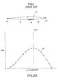
- FIG. 1 there is shown a diagrammatical representation of a conventional X-ray imaging system 10.
- the system 10 includes a point X-ray source 12 which directs a beam of X-rays 14 at a cone 16.
- a beam 18 is reflected off the inside surface of the cone 16 which is imaged on a spot 20.
- the cone 16 can be made from a number of materials and typically is made from a metal with a coating of platinum or tungsten.
- the X-rays in the beam 14 which arrive below the grazing incidence angle (Gg) are reflected by the cone 16 to the image point 20.
- Gg grazing incidence angle
- the intensity (R) of the X-ray beam 14 which is reflected from the cone 16 is directly proportional to the solid angle intersected by the cone 16 or other focusing device.
- the grazing incidence angle ( ⁇ g ) for the cone 16 is less than the angle of total internal reflection for the wavelength of interest.
- the angle ⁇ g for the cone 16 utilizing a W or a P+ coating is less than 1°. Therefore the solid angle intercepted and hence the collected X-ray intensity is very small.
- the focusing element is formed with a focusing surface from a section transverse to the axis of revolution of an ellipse. This involves defining the eccentricity of the ellipsoid, the focal separation and the optimum focusing surface.
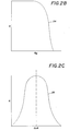
- This curve 22 is representative of the collection efficiency as a function of the equitorial angle ⁇ e .
- the angle ⁇ m of maximum collection efficiency can be solved as
- the product of curves 22 and 24 is taken which results in a curve 26 illustrated in Fig. 2C.
- the maximum value of the curve 26 defines the optimum angle ⁇ eB for an infinitesimal focusing surface of the ellipsoid.
- the 0 d spacing is 22.5A. All wavelengths which are substantially above ⁇ eB will not be reflected, i.e., the reflectivity R is zero.
- G eB is 12.7°.
- a point source 28 is selected of a size depending upon the application and then a finite segment length is chosen and the same segment length is moved along an ellipsoid surface 30 (only a portion of which is illustrated) about the median angle of 12.7°.
- the location of the point source 28 and a focus point 32 are defined by the foci of the ellipse.
- a 300 mm distance from the point source 28 to the focus point 32 was chosen.
- the flux contribution of two equal length finite segments 34 and 36 are illustrated by a flux contribution curve 38.
- the flux curve 38 represents the rate of change of flux ( ) collected by a perfectly reflecting ellipsoid surface. The curve 38 is determined without taking into account the effect of the layered coating. If the surface 30 was flat and included an appropriate layered coating, then a curve of flux collected vs. angle would result, similar to Fig. 2C.
- the coated surface 30 is an ellipsoid whose equitorial angle has been chosen to equal ⁇ eB with peak reflectance for Mg K ⁇
- a curve 40 results as illustrated in Fig. 2E.
- the curve 40 is the product of the substantially bell shaped flat coating curve (not illustrated) and the flux curve 38.
- the curve 40 represents the rate of change of flux ( ) collected by a coated reflecting ellipsoid surface in which the peak reflectance is 100% and whose peak reflectance angle coincides with the ellipsoid equator.
- Fig. 2F The effect of a shift of the angle of the peak reflectance to one side of the equitorial plane was then determined as illustrated in Fig. 2F.
- the flux resulting as a function of shift for a coating curve with a .5% width at half intensity is shown by a curve 42 and for a coating curve with a 1% width is shown by a curve 44.
- the layer coating can be graded through the structure to substantially retain the reflectance peak of the curve while increasing the width at the half intensity point.
- the width of the half intensity point can also be increased by decreasing the number of layer pairs at some loss in peak intensity.
- the layer coating can be graded across the structure to provide a high peak reflectance for the characteristic wavelength of interest at different positions on the surface of the ellipsoid by compensating for the change in incident angle at different points on the reflecting surface. Therefore, a slight shift in angle will not result in as large a magnitude decrease in reflectance as illustrated by coating curve 42.
- a total length along the coated ellipsoid of 200 mm was analyzed, 100 mm on each side of the equitorial plane. This gave a total collected flux curve 46 as illustrated by Fig. 2G.
- the curve 46 represents the curve 40 as the peak reflectance angle increases which expands and develops peaks 47 and 49 and a trough near the equitorial plane of the ellipsoid.
- the total effective length of an ellipsoidal section which would effectively collect all the flux is slightly over 80 mm in length. Therefore, for this example, the total focusing element length would be 80 mm if manufacturing considerations were ignored. As a practical manufacturing consideration, a section length of 30 mm was selected.
- This length was shifted along the length of the curve 46. It was determined that the maximum flux was collected for a section positioned with 27 mm on the source side of the equitorial angle and 3 mm on the focus side of the angle. As an alternate selection, the whole section was shifted to end 2 mm on the source side of the equitorial angle. This decreases the total reflected intensity only slightly, approximately 2% from the maximum attainable, as defined above. This can further facilitate the manufacturing of the focusing element and replication where desired as discussed with respect to Fig. 7.
- Fig. 3 illustrates a first embodiment of a focusing device 48 of the invention.
- the device includes a focusing element 50 which has a focusing surface 52 chosen in accordance with the technique described with respect to Figs. 2A-2G.
- the focusing surface 52 includes a plurality of layer pairs 54, only one pair of which is illustrated (Fig. 4). While only one layer pair 54 has been shown, having a single layer spacing d, typically many layer pairs are utilized for example on the order of 100-2000.
- the layer pairs also can have a graded d spacing as previously described.
- An incident X-ray beam 56 from a source 58 is made up of a band of wavelengths, ⁇ being an example of one wavelength.
- a beam dump would typically be utilized to prevent axial X-rays from impinging on a focus point 62.
- the focusing surface 52 is a portion of an ellipse 64 shown in phantom.
- the ellipse 64 is centered about the source 58 and the focus point 62 which define the foci of the ellipse 64.
- the ellipse 64 has a center line or plane 66 which also defines the equitorial angle O e . It could be assumed that the element 50 would be centered around the center plane 66, however, this is not the actual case as was described above.
- the element 50 is shifted toward the source 58 and, for example only, is illustrated shifted totally to the source side of the center line 66 essentially in the alternate position.
- a source 70 has a pair of conical incident beams 72 and 74 which are reflected by a respective one of a pair of focusing elements 76 and 78.
- Each of the focusing elements 76 and 78 has a respective focusing surface 80 and 82 which each reflects a respective beam 84 and 86 to a focus point 88.
- Adding the second element 78 or further elements increases the solid angle and hence, the total reflected X-ray intensity collected at the focus point 88.
- the d spacing of the layer pairs on the surface 80 is designed for angle 0 1
- the d spacing on the surface 82 is designed for angle 0 2 .
- Fig. 6 is a perspective view of a single focusing element 90 which has a focusing surface 92.
- the element or section 90 is designed as defined above for a specific width or element length "w" and has an inner diameter "id” in accordance with the ellipsoid chosen by the foci of 300 mm and the angle O e .
- the sections conveniently are formed of Al, Be or stainless steel which are diamond turned or conventionally machined and preferably are plated with electroless Ni and then polished.
- the sections could be formed of glass or other rigid substrate material.
- the layer pairs such as Hf:Si or W:Si are typically formed in ac - cordance with the methods described in the above referenced EPC application number 83 303 699.7.
- Fig. 7 illustrates a replication method of forming the focusing element 50 of the invention.
- a male section 94 is formed having a surface 96 which is a reverse or mirror image surface of the focusing surface 52 of the focusing element 50.
- a release coating 98 is then formed on the surface 96.
- a plurality of layer pairs 100 like the pairs 54, for example, are then formed on the release coating 98.
- a substrate 102 is then secured to the layer pairs 100 by a hardening filler 104, such as an epoxy type glue.
- the release coating 98 is then removed from the male section 94 and removed from the layer pairs 100 to replicate the element 50 and focusing surface 52 with the layer pairs 54 thereon.
- the male section 94 can be formed in one or more sections to facilitate removal of the release coating 98 of the structure formed thereon.
- the section 94 can then be utilized to form another focusing element. If the section 94 was formed for a focusing element 50 which includes the equitorial plane 66, the section 94 would have to be formed in pieces to remove the replicated section.
- Fig. 8 is a graphic illustration, not totally proportional which illustrates the significant difference in solid angle and hence total collected flux intensity between a prior art cone solid angle 106 and a focusing element solid angle 108 of the present invention.
- the layer pairs and the methods and materials forming them can be selected as desired; however, those described with respect to EPC application number 84 303 699.7 are preferred.
- the focusing elements and surfaces formed in accordance with the invention provide a substantial improvement in flux collected for any wavelength selected, substantially in the range of 0 0 2.8A to 120A, over grazing incidence devices.
- the reflectivity decreases as the wavelength increases to 120A; however, the solid angle increases to provide the enhanced performance. It is, therefore, to be understood that within the scope of the appended claims, the invention may be practiced otherwise than as specifically described.
Landscapes
- Engineering & Computer Science (AREA)
- Physics & Mathematics (AREA)
- Chemical & Material Sciences (AREA)
- Nanotechnology (AREA)
- Spectroscopy & Molecular Physics (AREA)
- General Engineering & Computer Science (AREA)
- High Energy & Nuclear Physics (AREA)
- Mathematical Physics (AREA)
- Theoretical Computer Science (AREA)
- Crystallography & Structural Chemistry (AREA)
- Optical Elements Other Than Lenses (AREA)
- Analysing Materials By The Use Of Radiation (AREA)
Applications Claiming Priority (2)
| Application Number | Priority Date | Filing Date | Title |
|---|---|---|---|
| US06/542,886 US4525853A (en) | 1983-10-17 | 1983-10-17 | Point source X-ray focusing device |
| US542886 | 1983-10-17 |
Publications (2)
| Publication Number | Publication Date |
|---|---|
| EP0138440A2 true EP0138440A2 (de) | 1985-04-24 |
| EP0138440A3 EP0138440A3 (de) | 1986-09-10 |
Family
ID=24165703
Family Applications (1)
| Application Number | Title | Priority Date | Filing Date |
|---|---|---|---|
| EP84306510A Withdrawn EP0138440A3 (de) | 1983-10-17 | 1984-09-24 | Fokussierungsvorrichtung für eine Röntgenstrahlungspunktquelle |
Country Status (7)
| Country | Link |
|---|---|
| US (1) | US4525853A (de) |
| EP (1) | EP0138440A3 (de) |
| JP (1) | JPS6098399A (de) |
| AU (1) | AU562603B2 (de) |
| CA (1) | CA1223092A (de) |
| IL (1) | IL72868A (de) |
| ZA (1) | ZA847129B (de) |
Cited By (3)
| Publication number | Priority date | Publication date | Assignee | Title |
|---|---|---|---|---|
| GB2175180A (en) * | 1985-05-14 | 1986-11-19 | Energy Conversion Devices Inc | Monochromatizing x-rays |
| WO1996002058A1 (en) * | 1994-07-08 | 1996-01-25 | Muradin Abubekirovich Kumakhov | Method of guiding beams of neutral and charged particles and a device for implementing said method |
| US7885372B2 (en) | 2007-12-07 | 2011-02-08 | Morpho Detection, Inc. | System and method for energy sensitive computed tomography |
Families Citing this family (40)
| Publication number | Priority date | Publication date | Assignee | Title |
|---|---|---|---|---|
| US4785470A (en) * | 1983-10-31 | 1988-11-15 | Ovonic Synthetic Materials Company, Inc. | Reflectivity and resolution X-ray dispersive and reflective structures for carbon, beryllium and boron analysis |
| US4941163A (en) * | 1985-08-15 | 1990-07-10 | The United States Of America As Represented By The Administrator Of The National Aeronautics And Space Administration | Multispectral glancing incidence X-ray telescope |
| DE3785763T2 (de) * | 1986-08-15 | 1993-10-21 | Commw Scient Ind Res Org | Instrumente zur konditionierung von röntgen- oder neutronenstrahlen. |
| US4989226A (en) * | 1987-08-21 | 1991-01-29 | Brigham Young University | Layered devices having surface curvature |
| NL8801019A (nl) * | 1988-04-20 | 1989-11-16 | Philips Nv | Roentgen spectrometer met dubbel gebogen kristal. |
| JPH0782117B2 (ja) * | 1989-02-23 | 1995-09-06 | オリンパス光学工業株式会社 | 反射型結像光学系 |
| JP2515893B2 (ja) * | 1989-10-26 | 1996-07-10 | オリンパス光学工業株式会社 | 結像型x線顕微鏡 |
| US5027377A (en) * | 1990-01-09 | 1991-06-25 | The United States Of America As Represented By The United States Department Of Energy | Chromatic X-ray magnifying method and apparatus by Bragg reflective planes on the surface of Abbe sphere |
| US5204887A (en) * | 1990-06-01 | 1993-04-20 | Canon Kabushiki Kaisha | X-ray microscope |
| US5646976A (en) * | 1994-08-01 | 1997-07-08 | Osmic, Inc. | Optical element of multilayered thin film for X-rays and neutrons |
| US5757882A (en) * | 1995-12-18 | 1998-05-26 | Osmic, Inc. | Steerable x-ray optical system |
| JP4160124B2 (ja) * | 1996-12-20 | 2008-10-01 | パナリティカル ビー ヴィ | 部分的に変化し、部分的に一定の曲率半径を有するアナライザ結晶を有するx線スペクトロメータ |
| US6014423A (en) * | 1998-02-19 | 2000-01-11 | Osmic, Inc. | Multiple corner Kirkpatrick-Baez beam conditioning optic assembly |
| JP3734366B2 (ja) | 1998-03-20 | 2006-01-11 | 株式会社リガク | X線分析装置 |
| US6069934A (en) * | 1998-04-07 | 2000-05-30 | Osmic, Inc. | X-ray diffractometer with adjustable image distance |
| US6094471A (en) * | 1998-04-22 | 2000-07-25 | Smithsonian Astrophysical Observatory | X-ray diagnostic system |
| DE10138313A1 (de) * | 2001-01-23 | 2002-07-25 | Zeiss Carl | Kollektor für Beleuchtugnssysteme mit einer Wellenlänge < 193 nm |
| GB9815968D0 (en) | 1998-07-23 | 1998-09-23 | Bede Scient Instr Ltd | X-ray focusing apparatus |
| DE19833524B4 (de) | 1998-07-25 | 2004-09-23 | Bruker Axs Gmbh | Röntgen-Analysegerät mit Gradienten-Vielfachschicht-Spiegel |
| US6389100B1 (en) | 1999-04-09 | 2002-05-14 | Osmic, Inc. | X-ray lens system |
| US6278764B1 (en) * | 1999-07-22 | 2001-08-21 | The Regents Of The Unviersity Of California | High efficiency replicated x-ray optics and fabrication method |
| US6421417B1 (en) | 1999-08-02 | 2002-07-16 | Osmic, Inc. | Multilayer optics with adjustable working wavelength |
| US6606371B2 (en) * | 1999-12-20 | 2003-08-12 | Agere Systems Inc. | X-ray system |
| US6504902B2 (en) | 2000-04-10 | 2003-01-07 | Rigaku Corporation | X-ray optical device and multilayer mirror for small angle scattering system |
| US6870896B2 (en) | 2000-12-28 | 2005-03-22 | Osmic, Inc. | Dark-field phase contrast imaging |
| US6804324B2 (en) * | 2001-03-01 | 2004-10-12 | Osmo, Inc. | X-ray phase contrast imaging using a fabry-perot interferometer concept |
| US6510200B1 (en) | 2001-06-29 | 2003-01-21 | Osmic, Inc. | Multi-layer structure with variable bandpass for monochromatization and spectroscopy |
| JP3762665B2 (ja) * | 2001-07-03 | 2006-04-05 | 株式会社リガク | X線分析装置およびx線供給装置 |
| US6643353B2 (en) | 2002-01-10 | 2003-11-04 | Osmic, Inc. | Protective layer for multilayers exposed to x-rays |
| JP3699998B2 (ja) * | 2002-03-20 | 2005-09-28 | 国立大学法人東北大学 | 蛍光x線ホログラフィー装置、蛍光x線ホログラフィーおよび局所構造解析方法 |
| US7245696B2 (en) * | 2002-05-29 | 2007-07-17 | Xradia, Inc. | Element-specific X-ray fluorescence microscope and method of operation |
| DE10254026C5 (de) * | 2002-11-20 | 2009-01-29 | Incoatec Gmbh | Reflektor für Röntgenstrahlung |
| GB0306829D0 (en) * | 2003-03-25 | 2003-04-30 | Oxford Diffraction Ltd | High flux x-ray source |
| WO2004114325A2 (en) * | 2003-06-13 | 2004-12-29 | Osmic, Inc. | Beam conditioning system |
| US7280634B2 (en) * | 2003-06-13 | 2007-10-09 | Osmic, Inc. | Beam conditioning system with sequential optic |
| JP4120502B2 (ja) * | 2003-07-14 | 2008-07-16 | 株式会社ニコン | 集光光学系、光源ユニット、照明光学装置および露光装置 |
| CN1918667A (zh) * | 2004-02-12 | 2007-02-21 | 独立行政法人科学技术振兴机构 | 软x射线加工装置以及软x射线加工方法 |
| US7068753B2 (en) * | 2004-07-30 | 2006-06-27 | Jordan Valley Applied Radiation Ltd. | Enhancement of X-ray reflectometry by measurement of diffuse reflections |
| US8369674B2 (en) * | 2009-05-20 | 2013-02-05 | General Electric Company | Optimizing total internal reflection multilayer optics through material selection |
| US8249220B2 (en) * | 2009-10-14 | 2012-08-21 | Rigaku Innovative Technologies, Inc. | Multiconfiguration X-ray optical system |
Family Cites Families (13)
| Publication number | Priority date | Publication date | Assignee | Title |
|---|---|---|---|---|
| US1865441A (en) * | 1923-08-04 | 1932-07-05 | Wappler Electric Company Inc | Method of and apparatus for controlling the direction of x-rays |
| US2759106A (en) * | 1951-05-25 | 1956-08-14 | Wolter Hans | Optical image-forming mirror system providing for grazing incidence of rays |
| US3010358A (en) * | 1959-02-19 | 1961-11-28 | Perkin Elmer Corp | Radiation microsampling apparatus |
| GB1045016A (en) * | 1964-01-24 | 1966-10-05 | Arthur Elliott | Improvements in or relating to mirrors |
| US3397312A (en) * | 1964-08-15 | 1968-08-13 | Hitachi Ltd | Laminated X-ray analyzing crystal wherein the respective laminations have different lattice spacings |
| NL7115946A (de) * | 1971-11-19 | 1973-05-22 | ||
| US3777156A (en) * | 1972-02-14 | 1973-12-04 | Hewlett Packard Co | Bent diffraction crystal with geometrical aberration compensation |
| US4084089A (en) * | 1976-12-20 | 1978-04-11 | North American Philips Corporation | Long wave-length X-ray diffraction crystal and method of manufacturing the same |
| US4229499A (en) * | 1978-06-23 | 1980-10-21 | North American Philips Corporation | Acid phthalate crystal |
| US4238265A (en) * | 1978-10-27 | 1980-12-09 | The Boeing Company | Method of manufacturing a glass parabolic-cylindrical solar collector |
| US4317043A (en) * | 1979-10-26 | 1982-02-23 | The University Of Rochester | Normal incidence x-ray reflectors and resonant cavities for supporting laser action using the same |
| US4261771A (en) * | 1979-10-31 | 1981-04-14 | Bell Telephone Laboratories, Incorporated | Method of fabricating periodic monolayer semiconductor structures by molecular beam epitaxy |
| CA1183285A (en) * | 1981-04-20 | 1985-02-26 | Robert K. Smither | Instrument and method for focusing x-rays, gamma rays and neutrons |
-
1983
- 1983-10-17 US US06/542,886 patent/US4525853A/en not_active Expired - Lifetime
-
1984
- 1984-09-05 IL IL72868A patent/IL72868A/xx unknown
- 1984-09-10 AU AU32880/84A patent/AU562603B2/en not_active Ceased
- 1984-09-11 ZA ZA847129A patent/ZA847129B/xx unknown
- 1984-09-18 CA CA000463475A patent/CA1223092A/en not_active Expired
- 1984-09-24 EP EP84306510A patent/EP0138440A3/de not_active Withdrawn
- 1984-09-25 JP JP59200339A patent/JPS6098399A/ja active Pending
Cited By (4)
| Publication number | Priority date | Publication date | Assignee | Title |
|---|---|---|---|---|
| GB2175180A (en) * | 1985-05-14 | 1986-11-19 | Energy Conversion Devices Inc | Monochromatizing x-rays |
| WO1996002058A1 (en) * | 1994-07-08 | 1996-01-25 | Muradin Abubekirovich Kumakhov | Method of guiding beams of neutral and charged particles and a device for implementing said method |
| US5744813A (en) * | 1994-07-08 | 1998-04-28 | Kumakhov; Muradin Abubekirovich | Method and device for controlling beams of neutral and charged particles |
| US7885372B2 (en) | 2007-12-07 | 2011-02-08 | Morpho Detection, Inc. | System and method for energy sensitive computed tomography |
Also Published As
| Publication number | Publication date |
|---|---|
| US4525853A (en) | 1985-06-25 |
| AU562603B2 (en) | 1987-06-11 |
| JPS6098399A (ja) | 1985-06-01 |
| ZA847129B (en) | 1985-06-26 |
| CA1223092A (en) | 1987-06-16 |
| IL72868A0 (en) | 1984-12-31 |
| AU3288084A (en) | 1985-04-26 |
| EP0138440A3 (de) | 1986-09-10 |
| IL72868A (en) | 1988-06-30 |
Similar Documents
| Publication | Publication Date | Title |
|---|---|---|
| EP0138440A2 (de) | Fokussierungsvorrichtung für eine Röntgenstrahlungspunktquelle | |
| EP0128026B1 (de) | Zerstreuende und reflektierende Strukturen für X-Strahlen mit verbesserter Reflexion und Auflösung und Herstellungsverfahren | |
| US5799056A (en) | Optical element of multilayered thin film for x-rays and neutrons | |
| JP3733142B2 (ja) | 操向可能のx線光学系 | |
| EP1234310B1 (de) | Zweifach gebogene optische vorrichtung mit gradierten atomaren schichten | |
| US4698833A (en) | Subassembly, method and system for monochromatizing X-rays | |
| US4675889A (en) | Multiple wavelength X-ray dispersive devices and method of making the devices | |
| US6226349B1 (en) | X-ray analysis apparatus with a graded multilayer mirror | |
| US4727000A (en) | X-ray dispersive and reflective structures | |
| EP1464061B1 (de) | Schutzschicht für der harten röntgenstrahlen ausgesetzte mehrschichten | |
| EP0876666A1 (de) | Kollimator fur rontgenstrahlungsspectroskopie | |
| US20050117239A1 (en) | Optical unit and associated method | |
| EP2433164B1 (de) | Optimierung interner totalspiegelung in mehrschicht optik durch auswahl der stoffe | |
| US7440546B2 (en) | Method of making and structure of multilayer laue lens for focusing hard x-rays | |
| US9082522B2 (en) | Zone compensated multilayer laue lens and apparatus and method of fabricating the same | |
| US4737973A (en) | Crystal monochromator | |
| US20050094271A1 (en) | Hybrid optical component for x ray applications and method associated therewith | |
| US5382342A (en) | Fabrication process for a gradient index x-ray lens | |
| US4317043A (en) | Normal incidence x-ray reflectors and resonant cavities for supporting laser action using the same | |
| CA1238988A (en) | X-ray dispersive and reflective structures and method of making the structures | |
| CA1333426C (en) | X-ray wave diffraction optics constructed by atomic layer epitaxy | |
| RU2104567C1 (ru) | Дифракционная решетка для ультрафиолетового и рентгеновского излучения | |
| Bradaczek et al. | Real X-ray optics-a challenge for crystal growers | |
| O'Hara | Nested parabolic reflective optics for laser plasmas |
Legal Events
| Date | Code | Title | Description |
|---|---|---|---|
| PUAI | Public reference made under article 153(3) epc to a published international application that has entered the european phase |
Free format text: ORIGINAL CODE: 0009012 |
|
| AK | Designated contracting states |
Designated state(s): AT BE CH DE FR GB IT LI LU NL SE |
|
| PUAL | Search report despatched |
Free format text: ORIGINAL CODE: 0009013 |
|
| AK | Designated contracting states |
Kind code of ref document: A3 Designated state(s): AT BE CH DE FR GB IT LI LU NL SE |
|
| 17P | Request for examination filed |
Effective date: 19870226 |
|
| 17Q | First examination report despatched |
Effective date: 19880707 |
|
| STAA | Information on the status of an ep patent application or granted ep patent |
Free format text: STATUS: THE APPLICATION IS DEEMED TO BE WITHDRAWN |
|
| 18D | Application deemed to be withdrawn |
Effective date: 19881118 |
|
| RIN1 | Information on inventor provided before grant (corrected) |
Inventor name: MARSHALL, GERALD FRANCIS Inventor name: KEEM, JOHN EDWARD |