EP0138517A1 - Integrierte Halbleiterschaltungen mit komplementären Metall-Oxyd-Halbleiteranordnungen - Google Patents
Integrierte Halbleiterschaltungen mit komplementären Metall-Oxyd-Halbleiteranordnungen Download PDFInfo
- Publication number
- EP0138517A1 EP0138517A1 EP84306756A EP84306756A EP0138517A1 EP 0138517 A1 EP0138517 A1 EP 0138517A1 EP 84306756 A EP84306756 A EP 84306756A EP 84306756 A EP84306756 A EP 84306756A EP 0138517 A1 EP0138517 A1 EP 0138517A1
- Authority
- EP
- European Patent Office
- Prior art keywords
- trench
- region
- substrate
- regions
- degrees
- Prior art date
- Legal status (The legal status is an assumption and is not a legal conclusion. Google has not performed a legal analysis and makes no representation as to the accuracy of the status listed.)
- Granted
Links
Images

Classifications
-
- H—ELECTRICITY
- H10—SEMICONDUCTOR DEVICES; ELECTRIC SOLID-STATE DEVICES NOT OTHERWISE PROVIDED FOR
- H10D—INORGANIC ELECTRIC SEMICONDUCTOR DEVICES
- H10D84/00—Integrated devices formed in or on semiconductor substrates that comprise only semiconducting layers, e.g. on Si wafers or on GaAs-on-Si wafers
- H10D84/80—Integrated devices formed in or on semiconductor substrates that comprise only semiconducting layers, e.g. on Si wafers or on GaAs-on-Si wafers characterised by the integration of at least one component covered by groups H10D12/00 or H10D30/00, e.g. integration of IGFETs
- H10D84/82—Integrated devices formed in or on semiconductor substrates that comprise only semiconducting layers, e.g. on Si wafers or on GaAs-on-Si wafers characterised by the integration of at least one component covered by groups H10D12/00 or H10D30/00, e.g. integration of IGFETs of only field-effect components
- H10D84/83—Integrated devices formed in or on semiconductor substrates that comprise only semiconducting layers, e.g. on Si wafers or on GaAs-on-Si wafers characterised by the integration of at least one component covered by groups H10D12/00 or H10D30/00, e.g. integration of IGFETs of only field-effect components of only insulated-gate FETs [IGFET]
- H10D84/85—Complementary IGFETs, e.g. CMOS
- H10D84/854—Complementary IGFETs, e.g. CMOS comprising arrangements for preventing bipolar actions between the different IGFET regions, e.g. arrangements for latchup prevention
-
- H—ELECTRICITY
- H10—SEMICONDUCTOR DEVICES; ELECTRIC SOLID-STATE DEVICES NOT OTHERWISE PROVIDED FOR
- H10W—GENERIC PACKAGES, INTERCONNECTIONS, CONNECTORS OR OTHER CONSTRUCTIONAL DETAILS OF DEVICES COVERED BY CLASS H10
- H10W10/00—Isolation regions in semiconductor bodies between components of integrated devices
- H10W10/01—Manufacture or treatment
- H10W10/041—Manufacture or treatment of isolation regions comprising polycrystalline semiconductor materials
-
- H—ELECTRICITY
- H10—SEMICONDUCTOR DEVICES; ELECTRIC SOLID-STATE DEVICES NOT OTHERWISE PROVIDED FOR
- H10W—GENERIC PACKAGES, INTERCONNECTIONS, CONNECTORS OR OTHER CONSTRUCTIONAL DETAILS OF DEVICES COVERED BY CLASS H10
- H10W10/00—Isolation regions in semiconductor bodies between components of integrated devices
- H10W10/40—Isolation regions comprising polycrystalline semiconductor materials
Definitions
- the invention pertains generally to semiconductor devices and, particularly, to integrated circuits containing complementary metal oxide semiconductor devices.
- CMOS integrated circuit devices include both n- and p-channel field effect transistors (FETs) on the same substrate. While, as known, it is generally desirable to space the different transistors as closely together as possible on the substrate, a limitation in the past is that if adjacent different type transistors (e.g., p and n channel field effect transistors) are too close together they can improperly electrically interact or "latchup" owing to the flow of leakage currents therebetween.
- FETs field effect transistors
- the trenches extend into or to a region of heavily doped semiconductor material providing a barrier to leakage currents between the trench-separated transistors.
- the presence of such leakage barrier reduces the depth of the trenches otherwise necessary.
- the invention is described in connection with an integrated circuit comprising a plurality of field-effect transistors disposed within a substrate of silicon.
- the trench filler material perferably comprises polycrystalline or amorphous silicon ("polysilicon” hereinafter) because such material can be readily deposited to completely fill a trench of proper design and because its coefficient of thermal expansion is the same as that of the silicon substrate. Both these conditions--complete, void-free filling and matching coefficient of expansion--are essential to avoid the prior art problem of excessive cracking of the trench-containing substrates.
- silicon dioxide While it is known in the past to fill trenches with polysilicon, silicon dioxide is also used, and no distinction has been made, as far as we know, between the two materials with respect to the cracking problem. Silicon dioxide, we have discovered, however, is not a suitable filler material with silicon substrates owing to the great disparity in the coefficients of thermal expansion of these materials.
- substrate-filler material combinations can be used. For example, it is possible to fill trenches in substrates of gallium arsenide with polycrystalline gallium arsenide deposited in known manner.
- filler materials can be used with non-identical substrate materials provided the coefficients of thermal expansion of the materials match within a factor of about 3.
- polysilicon is a good candidate for use as a filler material in substrates of gallium arsenide and similar III-IV compounds.
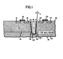
- a first embodiment of the inventive device depicted in FIG. 1, includes a substrate 20, of silicon, having a bulk region 30 of, for example, p - type conductivity (n-type conductivity is also useful) provided by a doping level ranging from about 10 15 cm -3 to about 10 17 cm -3 Doping levels less than about 10 15 cm -3 are undesirable because they require undesirably deep trenches to significantly reduce the possibility of latchup.
- the substrate 20 also includes a tub 40 of conductivity type opposite to that of the bulk region 30, e.g., n-type conductivity, extending from the surface 50.
- the depth of the tub 40 is preferably greater than about 1/2 m, while the vertical integrated doping level of the tub 40, i.e., the integral of the doping level of the tub 40 over the depth of the tub 40, ranges from about 10 12 to about 10 15 cm -2 , and is preferably about 10 13 cm -2 .
- a depth less than about 1/2 ⁇ m, and/or a vertical integrated doping level less than about 10 12 cm -2 often result in undesirable punchthrough from the source (of an FET formed in the tub 40) to the bulk region 30.
- the device includes a trench 140 which prevents, or substantially reduces the possibility of, latchup.
- the trench is formed in the silicon substrate 20, and separates the one or more p-channel FETs formed in the tub 40 from the one or more n-channel F ETs fabricated in the bulk region 30, i.e., the trench encircles the FETs in the tub 40.
- the trench 140 is formed after the fabrication of the tub 40 but before the fabrication of the FETs, and is preferably positioned at the juncture of the tub 40 and bulk region 30.
- a preferred filler material 160 is polysilicon which is readily deposited into the trench 140 using, for example, known conventional chemical vapor deposition (CVD) techniques.
- the angle (denoted a in FIG. 1) between the trench sidewall 150 and a perpendicular to the substrate surface 50 is between about 5 to 10 degrees. It is found that trenches having steeper (e.g., vertical) walls or, worse, negative angle walls (e.g., trenches which widen towards the bottom) are quite difficult to completely fill. The diverging trench walls avoid any masking effects, by the walls, of the filler material during the deposition process. Conversely, trenches having wall angles in excess of 10 degrees become too wide, thus defeating the object of small transitor spacings.
- the second condition is that the thickness of the polysilicon deposited in the trench filling process is adequate to at least completely fill the trench. To ensure this result, a thickness which is slightly excessive is used, and the excessive material overlying the trench is slightly etched back using known processes.
- the trench 140 preferably includes a relatively thin layer of a dielectric material (material whose bandgap is greater than about 2 eV) 170 covering the interior surfaces of the trench.
- a dielectric material material whose bandgap is greater than about 2 eV
- Useful dielectric materials include Sio 2 and Si 3 N 4 deposited in known fashion.
- the thickness of the dielectric layer 170 ranges from about 200 Angstroms (A) to about 5000 A. A thickness less than about 200 A is undesirable as being ineffective to prevent short circuits through the polysilicon.
- a thickness greater than about 5000 A is undesirable as resulting in the formation of cracks and dislocations at the coating 170-trench wall 150 interface during high temperature processing.
- the etching of the substrate to form the trenches is done by a known reactive-ion-etching process.
- the angle of slope of the trench walls can be selected.
- a second embodiment of the inventive device differs from the first embodiment in that the substrate.20 includes a relatively heavily doped bulk region 32 of, for example, p-type conductivity, supporting a moderately doped, relatively thin (compared to the bulk region 32) layer 34 whose conductivity type is the same as that of the region 32.
- the layer 34 is preferably epitaxially grown on the bulk region 32 using, for example, conventional vapor phase epitaxy.
- a tub 40 of, for example, n-type conductivity, is formed in the moderately doped layer 34 and a trench 140 extends through the thickness of the layer 34 at least to the heavily doped bulk region 32.
- the advantage of this arrangement is that the depth of the trench 140 is reduced (as compared to the trench employed in the first embodiment) because the heavy doping within the bulk region 32 reduces the lifetime of minority charge carriers therethrough which would otherwise cause latchup between the two MOS devices shown.
- the doping level within the bulk region 32 ranges from about 10 17 to about 10 21 cm -3 , and is preferably about 10 20 cm -3 .
- a doping level less than about 10 17 cm -3 is undesirable because so low a doping level does not significantly reduce the possibility of latchup.
- a doping level greater than about 10 21 cm -3 is undesirable because so high a doping level results in an undesirably large out-diffusion of dopant from the bulk region 32 into the layer 34.
- the layer 34 has a thickness ranging from about 1 ⁇ m to about 10 ⁇ m, and a doping level ranging from about 10 14 to about 10 17 cm -3 .
- the tub 40 has a thickness greater than about 1/2 ⁇ m but less than the thickness of the layer 34, and a vertical integrated doping level ranging from about 10 12 to about 10 15 cm -2 .
- a third embodiment of the inventive device is generally similar to the second embodiment except that the depth of the trench 140 is reduced by the depth of a relatively heavily doped region 190 within the layer 34, extending from the bottom of the trench into.the bulk region 32.
- the conductivity type and the doping level range for the region 190 is the same as that for the bulk region 32, and thus the region 190 is essentially an extension of the bulk region 32 into the layer 34.
- the region 190 serves the same purpose as the bulk region 32, i.e., it reduces the lifetime of minority carriers therethrough (while decreasing trench depth).
- the region 190 is formed by implanting donor or acceptor ions (depending on whether the region 190 is to be of n ⁇ or p +- type conductivity) into the semiconductor material adjacent the bottom of the trench, and then diffusing these ions toward the bulk region 32 with a heat treatment. Because ions diffuse both vertically and laterally, vertical diffusion, and thus the depth of region 190, is preferably less than about 4 ⁇ m to avoid undesirable lateral diffusion of dopant into the tub 40.
- Ion implantation preferably occurs after the formation of the dielectric layer 170 on the walls of the trench 140 (and before the deposition of the polysilicon). Because the trench sidewall 150 is inclined to the vertical (as viewed in FIG. 4), and because the ions travel an essentially vertical path, the ions impinging the sidewall of the trench must penetrate a greater thickness of dielectric material than the ions impinging the bottom of the trench to reach the underlying semiconductor material. Thus, relatively few, if any, ions penetrate the sidewall 150 into the tub 40.
- dopant implantation levels range from about 1 0 14 to about 10 17 cm -2 .
- An implantation level less than about 1014cm-2 is undesirable because this results in an undesirably low dopant concentration (dopant per unit volume) in the region 190.
- An implantation level greater than about 1017cm-2 is undesirable because so great an implantation level is more than is required to achieve the desired dopant concentration, and requires an undesirably long time to achieve.
Landscapes
- Metal-Oxide And Bipolar Metal-Oxide Semiconductor Integrated Circuits (AREA)
- Element Separation (AREA)
Applications Claiming Priority (4)
| Application Number | Priority Date | Filing Date | Title |
|---|---|---|---|
| US54062383A | 1983-10-11 | 1983-10-11 | |
| US54062483A | 1983-10-11 | 1983-10-11 | |
| US540623 | 1983-10-11 | ||
| US540624 | 1983-10-11 |
Publications (2)
| Publication Number | Publication Date |
|---|---|
| EP0138517A1 true EP0138517A1 (de) | 1985-04-24 |
| EP0138517B1 EP0138517B1 (de) | 1988-07-06 |
Family
ID=27066485
Family Applications (2)
| Application Number | Title | Priority Date | Filing Date |
|---|---|---|---|
| EP84903741A Pending EP0158670A1 (de) | 1983-10-11 | 1984-10-04 | Integrierte halbleiterschaltungen mit komplementären metalloxid-halbleiteranordnungen |
| EP84306756A Expired EP0138517B1 (de) | 1983-10-11 | 1984-10-04 | Integrierte Halbleiterschaltungen mit komplementären Metall-Oxyd-Halbleiteranordnungen |
Family Applications Before (1)
| Application Number | Title | Priority Date | Filing Date |
|---|---|---|---|
| EP84903741A Pending EP0158670A1 (de) | 1983-10-11 | 1984-10-04 | Integrierte halbleiterschaltungen mit komplementären metalloxid-halbleiteranordnungen |
Country Status (4)
| Country | Link |
|---|---|
| EP (2) | EP0158670A1 (de) |
| KR (1) | KR850700087A (de) |
| DE (1) | DE3472604D1 (de) |
| WO (1) | WO1985001836A1 (de) |
Cited By (10)
| Publication number | Priority date | Publication date | Assignee | Title |
|---|---|---|---|---|
| WO1986003339A1 (en) * | 1984-11-23 | 1986-06-05 | American Telephone & Telegraph Company | Method for fabricating semiconductor devices and devices formed thereby |
| DE3625742A1 (de) * | 1985-08-05 | 1987-05-27 | Rca Corp | Integrierte cmos-schaltung und verfahren zum herstellen der schaltung |
| GB2183907A (en) * | 1985-11-27 | 1987-06-10 | Raytheon Co | Reducing radiation effects on integrated circuits |
| EP0236123A3 (de) * | 1986-03-04 | 1988-07-20 | Seiko Epson Corporation | Halbleiteranordnung und Verfahren zum Herstellen derselben |
| FR2633777A1 (fr) * | 1988-06-30 | 1990-01-05 | Goldstar Semiconductor Ltd | Cellule eprom utilisant un isolement de tranchee et son procede de fabrication |
| EP0242506A3 (en) * | 1986-03-17 | 1990-03-14 | International Business Machines Corporation | Sidewall spacers for cmos circuits stress relief/isolation and method for making |
| US4936928A (en) * | 1985-11-27 | 1990-06-26 | Raytheon Company | Semiconductor device |
| EP0382865A1 (de) * | 1989-02-14 | 1990-08-22 | Siemens Aktiengesellschaft | Anordnung zur Verminderung von Latch-up-Störanfälligkeit bei CMOS-Halbleiterschaltungen |
| US5296397A (en) * | 1988-06-30 | 1994-03-22 | Goldstar Electron Co., Ltd. | Method for manufacturing an EPROM cell |
| US6642175B2 (en) | 2000-10-03 | 2003-11-04 | Fuji Photo Film Co., Ltd. | Heat-sensitive recording material |
Citations (1)
| Publication number | Priority date | Publication date | Assignee | Title |
|---|---|---|---|---|
| EP0048175A2 (de) * | 1980-09-17 | 1982-03-24 | Hitachi, Ltd. | Halbleiterbauelement und Verfahren zu dessen Herstellung |
Family Cites Families (1)
| Publication number | Priority date | Publication date | Assignee | Title |
|---|---|---|---|---|
| US4486266A (en) * | 1983-08-12 | 1984-12-04 | Tektronix, Inc. | Integrated circuit method |
-
1984
- 1984-10-04 WO PCT/US1984/001583 patent/WO1985001836A1/en not_active Ceased
- 1984-10-04 EP EP84903741A patent/EP0158670A1/de active Pending
- 1984-10-04 DE DE8484306756T patent/DE3472604D1/de not_active Expired
- 1984-10-04 KR KR1019850700081A patent/KR850700087A/ko not_active Ceased
- 1984-10-04 EP EP84306756A patent/EP0138517B1/de not_active Expired
Patent Citations (1)
| Publication number | Priority date | Publication date | Assignee | Title |
|---|---|---|---|---|
| EP0048175A2 (de) * | 1980-09-17 | 1982-03-24 | Hitachi, Ltd. | Halbleiterbauelement und Verfahren zu dessen Herstellung |
Non-Patent Citations (1)
| Title |
|---|
| INTERNATIONAL ELECTRON DEVICES MEETING, San Francisco, 13th-15th December 1982, Technical Digest, pages 237-240, IEEE, New York, USA; R.D. RUNG et al.: "Deep trench isolated CMOS devices" * |
Cited By (14)
| Publication number | Priority date | Publication date | Assignee | Title |
|---|---|---|---|---|
| WO1986003339A1 (en) * | 1984-11-23 | 1986-06-05 | American Telephone & Telegraph Company | Method for fabricating semiconductor devices and devices formed thereby |
| DE3625742A1 (de) * | 1985-08-05 | 1987-05-27 | Rca Corp | Integrierte cmos-schaltung und verfahren zum herstellen der schaltung |
| GB2183907B (en) * | 1985-11-27 | 1989-10-04 | Raytheon Co | Semiconductor device |
| DE3640438A1 (de) * | 1985-11-27 | 1987-07-02 | Raytheon Co | Halbleitergeraet |
| GB2183907A (en) * | 1985-11-27 | 1987-06-10 | Raytheon Co | Reducing radiation effects on integrated circuits |
| US4936928A (en) * | 1985-11-27 | 1990-06-26 | Raytheon Company | Semiconductor device |
| EP0236123A3 (de) * | 1986-03-04 | 1988-07-20 | Seiko Epson Corporation | Halbleiteranordnung und Verfahren zum Herstellen derselben |
| US4826781A (en) * | 1986-03-04 | 1989-05-02 | Seiko Epson Corporation | Semiconductor device and method of preparation |
| EP0242506A3 (en) * | 1986-03-17 | 1990-03-14 | International Business Machines Corporation | Sidewall spacers for cmos circuits stress relief/isolation and method for making |
| FR2633777A1 (fr) * | 1988-06-30 | 1990-01-05 | Goldstar Semiconductor Ltd | Cellule eprom utilisant un isolement de tranchee et son procede de fabrication |
| NL8901545A (nl) * | 1988-06-30 | 1990-01-16 | Goldstar Semiconductor Ltd | Eprom-cel met gleuf-isolatie, en werkwijze voor het vervaardigen hiervan. |
| US5296397A (en) * | 1988-06-30 | 1994-03-22 | Goldstar Electron Co., Ltd. | Method for manufacturing an EPROM cell |
| EP0382865A1 (de) * | 1989-02-14 | 1990-08-22 | Siemens Aktiengesellschaft | Anordnung zur Verminderung von Latch-up-Störanfälligkeit bei CMOS-Halbleiterschaltungen |
| US6642175B2 (en) | 2000-10-03 | 2003-11-04 | Fuji Photo Film Co., Ltd. | Heat-sensitive recording material |
Also Published As
| Publication number | Publication date |
|---|---|
| DE3472604D1 (en) | 1988-08-11 |
| EP0138517B1 (de) | 1988-07-06 |
| EP0158670A1 (de) | 1985-10-23 |
| WO1985001836A1 (en) | 1985-04-25 |
| KR850700087A (ko) | 1985-10-21 |
Similar Documents
| Publication | Publication Date | Title |
|---|---|---|
| JP3544833B2 (ja) | 半導体装置及びその製造方法 | |
| US7112519B2 (en) | Semiconductor device manufacturing method | |
| US5401998A (en) | Trench isolation using doped sidewalls | |
| US6255152B1 (en) | Method of fabricating CMOS using Si-B layer to form source/drain extension junction | |
| US6320225B1 (en) | SOI CMOS body contact through gate, self-aligned to source- drain diffusions | |
| US6410938B1 (en) | Semiconductor-on-insulator device with nitrided buried oxide and method of fabricating | |
| US6773995B2 (en) | Double diffused MOS transistor and method for manufacturing same | |
| US4711017A (en) | Formation of buried diffusion devices | |
| US5148247A (en) | Semiconductor device having trench isolation | |
| US6548866B2 (en) | Field effect transistor with reduced narrow channel effect | |
| US5580799A (en) | Method of manufacturing transistor with channel implant | |
| US5250837A (en) | Method for dielectrically isolating integrated circuits using doped oxide sidewalls | |
| KR20000065719A (ko) | 반도체 소자 및 그 제조방법 | |
| US4992838A (en) | Vertical MOS transistor with threshold voltage adjustment | |
| JPH0680724B2 (ja) | 絶縁分離のcmos fet集積装置の製造方法 | |
| JP7145313B2 (ja) | 半導体デバイス及びその製造方法 | |
| US4900689A (en) | Method of fabrication of isolated islands for complementary bipolar devices | |
| EP0138517B1 (de) | Integrierte Halbleiterschaltungen mit komplementären Metall-Oxyd-Halbleiteranordnungen | |
| US5932913A (en) | MOS transistor with controlled shallow source/drain junction, source/drain strap portions, and source/drain electrodes on field insulation layers | |
| US6274442B1 (en) | Transistor having a nitrogen incorporated epitaxially grown gate dielectric and method of making same | |
| US6043544A (en) | Semiconductor gate conductor with a substantially uniform doping profile having minimal susceptibility to dopant penetration into the underlying gate dielectric | |
| US20020182831A1 (en) | Semiconductor device and method of manufacturing the same | |
| US8816429B2 (en) | Charge balance semiconductor devices with increased mobility structures | |
| US6235610B1 (en) | Process for selectively implanting dopants into the bottom of a deep trench | |
| US6482719B1 (en) | Semiconductor field region implant methodology |
Legal Events
| Date | Code | Title | Description |
|---|---|---|---|
| PUAI | Public reference made under article 153(3) epc to a published international application that has entered the european phase |
Free format text: ORIGINAL CODE: 0009012 |
|
| AK | Designated contracting states |
Designated state(s): IT |
|
| 17P | Request for examination filed |
Effective date: 19850925 |
|
| 17Q | First examination report despatched |
Effective date: 19861031 |
|
| RBV | Designated contracting states (corrected) |
Designated state(s): CH DE FR GB IT LI NL |
|
| XX | Miscellaneous (additional remarks) |
Free format text: VERBUNDEN MIT 84903741.1/0158670 (EUROPAEISCHE ANMELDENUMMER/VEROEFFENTLICHUNGSNUMMER) DURCH ENTSCHEIDUNG VOM 27.08.87. |
|
| GRAA | (expected) grant |
Free format text: ORIGINAL CODE: 0009210 |
|
| AK | Designated contracting states |
Kind code of ref document: B1 Designated state(s): CH DE FR GB IT LI NL |
|
| XX | Miscellaneous (additional remarks) |
Free format text: VERBUNDEN MIT 84903741.1/0158670 (EUROPAEISCHE ANMELDENUMMER/VEROEFFENTLICHUNGSNUMMER) DURCH ENTSCHEIDUNG VOM 27.08.87. |
|
| ITF | It: translation for a ep patent filed | ||
| REF | Corresponds to: |
Ref document number: 3472604 Country of ref document: DE Date of ref document: 19880811 |
|
| ET | Fr: translation filed | ||
| PLBI | Opposition filed |
Free format text: ORIGINAL CODE: 0009260 |
|
| 26 | Opposition filed |
Opponent name: TELEFUNKEN ELECTRONIC GMBH Effective date: 19890405 |
|
| NLR1 | Nl: opposition has been filed with the epo |
Opponent name: TELEFUNKEN ELECTRONIC GMBH |
|
| PGFP | Annual fee paid to national office [announced via postgrant information from national office to epo] |
Ref country code: DE Payment date: 19900921 Year of fee payment: 7 |
|
| PGFP | Annual fee paid to national office [announced via postgrant information from national office to epo] |
Ref country code: GB Payment date: 19900927 Year of fee payment: 7 |
|
| PGFP | Annual fee paid to national office [announced via postgrant information from national office to epo] |
Ref country code: CH Payment date: 19901001 Year of fee payment: 7 |
|
| ITTA | It: last paid annual fee | ||
| PGFP | Annual fee paid to national office [announced via postgrant information from national office to epo] |
Ref country code: NL Payment date: 19901031 Year of fee payment: 7 |
|
| RDAG | Patent revoked |
Free format text: ORIGINAL CODE: 0009271 |
|
| STAA | Information on the status of an ep patent application or granted ep patent |
Free format text: STATUS: PATENT REVOKED |
|
| PGFP | Annual fee paid to national office [announced via postgrant information from national office to epo] |
Ref country code: FR Payment date: 19910917 Year of fee payment: 8 |
|
| REG | Reference to a national code |
Ref country code: CH Ref legal event code: PL |
|
| 27W | Patent revoked |
Effective date: 19910825 |
|
| GBPR | Gb: patent revoked under art. 102 of the ep convention designating the uk as contracting state | ||
| NLR2 | Nl: decision of opposition | ||
| APAH | Appeal reference modified |
Free format text: ORIGINAL CODE: EPIDOSCREFNO |