EP0138672A2 - Méthode pour la fabrication d'une plaquette à circuit imprimé - Google Patents
Méthode pour la fabrication d'une plaquette à circuit imprimé Download PDFInfo
- Publication number
- EP0138672A2 EP0138672A2 EP84401853A EP84401853A EP0138672A2 EP 0138672 A2 EP0138672 A2 EP 0138672A2 EP 84401853 A EP84401853 A EP 84401853A EP 84401853 A EP84401853 A EP 84401853A EP 0138672 A2 EP0138672 A2 EP 0138672A2
- Authority
- EP
- European Patent Office
- Prior art keywords
- substrate
- powder
- passage
- electrically conductive
- circuit board
- Prior art date
- Legal status (The legal status is an assumption and is not a legal conclusion. Google has not performed a legal analysis and makes no representation as to the accuracy of the status listed.)
- Withdrawn
Links
- 238000004519 manufacturing process Methods 0.000 title claims description 9
- 239000000758 substrate Substances 0.000 claims abstract description 56
- 239000000843 powder Substances 0.000 claims abstract description 50
- 238000000034 method Methods 0.000 claims abstract description 20
- 238000003825 pressing Methods 0.000 claims abstract description 10
- 238000010438 heat treatment Methods 0.000 claims abstract description 8
- 230000002411 adverse Effects 0.000 claims abstract description 7
- 239000002184 metal Substances 0.000 claims description 10
- 229910052751 metal Inorganic materials 0.000 claims description 10
- RYGMFSIKBFXOCR-UHFFFAOYSA-N Copper Chemical group [Cu] RYGMFSIKBFXOCR-UHFFFAOYSA-N 0.000 claims description 5
- ATJFFYVFTNAWJD-UHFFFAOYSA-N Tin Chemical group [Sn] ATJFFYVFTNAWJD-UHFFFAOYSA-N 0.000 claims description 5
- 229910052802 copper Inorganic materials 0.000 claims description 5
- 239000010949 copper Substances 0.000 claims description 5
- 239000000428 dust Substances 0.000 claims description 5
- 238000000137 annealing Methods 0.000 claims description 4
- 239000000463 material Substances 0.000 description 6
- 239000004020 conductor Substances 0.000 description 5
- 239000000126 substance Substances 0.000 description 5
- 239000004697 Polyetherimide Substances 0.000 description 3
- 239000004033 plastic Substances 0.000 description 3
- 229920003023 plastic Polymers 0.000 description 3
- 229920001601 polyetherimide Polymers 0.000 description 3
- 238000005452 bending Methods 0.000 description 2
- 239000002245 particle Substances 0.000 description 2
- 239000000654 additive Substances 0.000 description 1
- 230000000996 additive effect Effects 0.000 description 1
- 239000000919 ceramic Substances 0.000 description 1
- 239000002894 chemical waste Substances 0.000 description 1
- 238000005336 cracking Methods 0.000 description 1
- 238000000151 deposition Methods 0.000 description 1
- 239000003989 dielectric material Substances 0.000 description 1
- 239000006185 dispersion Substances 0.000 description 1
- 238000005553 drilling Methods 0.000 description 1
- 230000000694 effects Effects 0.000 description 1
- 239000011213 glass-filled polymer Substances 0.000 description 1
- 238000002347 injection Methods 0.000 description 1
- 239000007924 injection Substances 0.000 description 1
- 238000001746 injection moulding Methods 0.000 description 1
- 239000007788 liquid Substances 0.000 description 1
- 229910001092 metal group alloy Inorganic materials 0.000 description 1
- 239000002923 metal particle Substances 0.000 description 1
- 238000007747 plating Methods 0.000 description 1
- 239000012255 powdered metal Substances 0.000 description 1
- 238000003892 spreading Methods 0.000 description 1
- 239000002699 waste material Substances 0.000 description 1
Images
Classifications
-
- H—ELECTRICITY
- H05—ELECTRIC TECHNIQUES NOT OTHERWISE PROVIDED FOR
- H05K—PRINTED CIRCUITS; CASINGS OR CONSTRUCTIONAL DETAILS OF ELECTRIC APPARATUS; MANUFACTURE OF ASSEMBLAGES OF ELECTRICAL COMPONENTS
- H05K3/00—Apparatus or processes for manufacturing printed circuits
- H05K3/40—Forming printed elements for providing electric connections to or between printed circuits
- H05K3/4038—Through-connections; Vertical interconnect access [VIA] connections
- H05K3/4053—Through-connections; Vertical interconnect access [VIA] connections by thick-film techniques
- H05K3/4069—Through-connections; Vertical interconnect access [VIA] connections by thick-film techniques for via connections in organic insulating substrates
-
- H—ELECTRICITY
- H05—ELECTRIC TECHNIQUES NOT OTHERWISE PROVIDED FOR
- H05K—PRINTED CIRCUITS; CASINGS OR CONSTRUCTIONAL DETAILS OF ELECTRIC APPARATUS; MANUFACTURE OF ASSEMBLAGES OF ELECTRICAL COMPONENTS
- H05K3/00—Apparatus or processes for manufacturing printed circuits
- H05K3/10—Apparatus or processes for manufacturing printed circuits in which conductive material is applied to the insulating support in such a manner as to form the desired conductive pattern
- H05K3/102—Apparatus or processes for manufacturing printed circuits in which conductive material is applied to the insulating support in such a manner as to form the desired conductive pattern by bonding of conductive powder, i.e. metallic powder
-
- H—ELECTRICITY
- H05—ELECTRIC TECHNIQUES NOT OTHERWISE PROVIDED FOR
- H05K—PRINTED CIRCUITS; CASINGS OR CONSTRUCTIONAL DETAILS OF ELECTRIC APPARATUS; MANUFACTURE OF ASSEMBLAGES OF ELECTRICAL COMPONENTS
- H05K1/00—Printed circuits
- H05K1/02—Details
- H05K1/03—Use of materials for the substrate
- H05K1/0306—Inorganic insulating substrates, e.g. ceramic, glass
-
- H—ELECTRICITY
- H05—ELECTRIC TECHNIQUES NOT OTHERWISE PROVIDED FOR
- H05K—PRINTED CIRCUITS; CASINGS OR CONSTRUCTIONAL DETAILS OF ELECTRIC APPARATUS; MANUFACTURE OF ASSEMBLAGES OF ELECTRICAL COMPONENTS
- H05K2201/00—Indexing scheme relating to printed circuits covered by H05K1/00
- H05K2201/09—Shape and layout
- H05K2201/09009—Substrate related
- H05K2201/09118—Moulded substrate
-
- H—ELECTRICITY
- H05—ELECTRIC TECHNIQUES NOT OTHERWISE PROVIDED FOR
- H05K—PRINTED CIRCUITS; CASINGS OR CONSTRUCTIONAL DETAILS OF ELECTRIC APPARATUS; MANUFACTURE OF ASSEMBLAGES OF ELECTRICAL COMPONENTS
- H05K2203/00—Indexing scheme relating to apparatus or processes for manufacturing printed circuits covered by H05K3/00
- H05K2203/01—Tools for processing; Objects used during processing
- H05K2203/0104—Tools for processing; Objects used during processing for patterning or coating
- H05K2203/0108—Male die used for patterning, punching or transferring
-
- H—ELECTRICITY
- H05—ELECTRIC TECHNIQUES NOT OTHERWISE PROVIDED FOR
- H05K—PRINTED CIRCUITS; CASINGS OR CONSTRUCTIONAL DETAILS OF ELECTRIC APPARATUS; MANUFACTURE OF ASSEMBLAGES OF ELECTRICAL COMPONENTS
- H05K2203/00—Indexing scheme relating to apparatus or processes for manufacturing printed circuits covered by H05K3/00
- H05K2203/02—Details related to mechanical or acoustic processing, e.g. drilling, punching, cutting, using ultrasound
- H05K2203/0278—Flat pressure, e.g. for connecting terminals with anisotropic conductive adhesive
-
- H—ELECTRICITY
- H05—ELECTRIC TECHNIQUES NOT OTHERWISE PROVIDED FOR
- H05K—PRINTED CIRCUITS; CASINGS OR CONSTRUCTIONAL DETAILS OF ELECTRIC APPARATUS; MANUFACTURE OF ASSEMBLAGES OF ELECTRICAL COMPONENTS
- H05K2203/00—Indexing scheme relating to apparatus or processes for manufacturing printed circuits covered by H05K3/00
- H05K2203/11—Treatments characterised by their effect, e.g. heating, cooling, roughening
- H05K2203/1131—Sintering, i.e. fusing of metal particles to achieve or improve electrical conductivity
-
- H—ELECTRICITY
- H05—ELECTRIC TECHNIQUES NOT OTHERWISE PROVIDED FOR
- H05K—PRINTED CIRCUITS; CASINGS OR CONSTRUCTIONAL DETAILS OF ELECTRIC APPARATUS; MANUFACTURE OF ASSEMBLAGES OF ELECTRICAL COMPONENTS
- H05K3/00—Apparatus or processes for manufacturing printed circuits
- H05K3/10—Apparatus or processes for manufacturing printed circuits in which conductive material is applied to the insulating support in such a manner as to form the desired conductive pattern
- H05K3/107—Apparatus or processes for manufacturing printed circuits in which conductive material is applied to the insulating support in such a manner as to form the desired conductive pattern by filling grooves in the support with conductive material
Definitions
- This invention relates to a printed circuit board and more particularly to a dry additive process for providing an electrically conductive path through a circuit board.
- Each circuit board is comprised of a dielectric substrate having on one or both sides a plurality of electrically conductive paths, arranged in a predetermined manner, to connect together circuit elements mounted to the substrate.
- a conductive path on each side of the substrate may be connected together by one or more conductors traversing the edge of the board between the sides or by a metal eyelet located in a hole in the board.
- One example of a circuit board with metal eyelets may be found in U.S. Patent 3,731,252 entitled "Printed Circuit Board Connector" and issued May 1, 1973.
- the conductive paths may be placed on the substrate by the application of a metal conductor to the substrate and the subsequent removal of portions of the conductor by liquid chemicals or by depositing an electrical conductor on the substrate with chemical plating baths.
- Examples of other methods of making circuit boards may be found in U.S. Patents 4,327,124 entitled “Method for Manufacturing Printed Circuits Comprising Printing Conductive Ink on Dielectric Surface” issued April 27, 1982; and 3,013,913 entitled “Molded Printed Circuit,” issued December 19, 1961.
- wastes are a problem as they must be disposed of without adversely affecting our environment. Further, the methods using chemicals are expensive and relatively complex.
- the resulting conductive path has material from the substrate dispersed within the conductor lowering its conductivity. This is not acceptable for certain circuit board applications.
- using metal eyelets to connect conductive paths on opposite sides of a circuit board requires an extra step in the manufacturing process and hence increases the cost of making the board.
- the use of a metal eyelet limits the minimum diameter of a passage through a circuit board.
- This invention is a method for making a conductive path through a circuit board to connect together the electrically conducting paths on opposite sides of the circuit board.
- the invention is characterized by the steps of forming a passage through a circuit board that connects to a conductive path on each side of the circuit board, filling the passage in the substrate with an electrically conductive powder, applying pressure to compact the powder in the passage of the substrate, and then heating the compacted powder to its isothermal annealing temperature to increase the conductivity and ductility of the compacted powder and its adhesion to the substrate without adversely affecting the shape or condition of the substrate.
- the heating step may be omitted when the compacted powder is a metal such as tin.
- An advantage of the method is that it does not require the use of chemicals and hence eliminates chemical wastes, which if not treated properly would provide a hazard to our environment.
- Another advantage of the invention is that it reduces the complexity and expense of manufacturing a circuit board.
- Another advantage of the invention is that the conductive paths on a circuit board and the conductive passages through a circuit board may be made in one operation.
- Another advantage of the invention is that it provides a method of making a conductive path through a circuit board.
- Another advantage of the invention is that it provides a method of making a conductive path through a substrate that can have a smaller diameter than required by a metal eyelet.
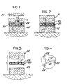
- FIGURES 1 through 4 illustrate a method of applying pressure, by a die 30 to an electrically conductive powder 10 in the passage 21 of a substrate 20 to provide a compacted powder 11 in the passage 21 that connects to conductive paths 25 on the substrate 20.
- Step 1 is the forming of at least one passage 21 through a substrate 20 having electrically conductive paths 25 on opposite sides of the substrate 20.
- the passage 21 may be made by injection molding a substrate with a passage, drilling a passage into the substrate, or by stamping the substrate with a die to form the passage.
- the passage 21 is located so as to connect to ' predetermined conductive paths 25 on opposite sides of the substrate 20.
- a preferable material for such a substrate would be a plastic such as polyetherimide. Other dielectric materials such as a glass filled plastic or a ceramic may be used.
- a polyetherimide substrate 20 is injection molded to have a passage 21 and grooves on both sides.
- Step 2 is the filling or over filling of the passage 21 and any grooves in the substrate 20 with an electrically conductive powder 10.
- the electrically conductive powder 10 may be a metal or metal alloy such - ⁇ -as a copper electrolytic dust which has a particle size less than about 100 microns and is flaky and irregularly shaped.
- Step 3 is the application of pressure with die 30 to the electrically conductive powder 10 to provide a compacted powder 11 in the passage 21. Spreading additional powder 10 and compacting it may be accomplished if a thicker compacted powder 11 is desired. The pressure applied may vary depending upon the materials chosen for the conductive powder 10 and the substrate 20.
- the pressure applied is the highest pressure possible that can be applied to the electrically conductive powder 10 without adversely affecting the substrate 20.
- adverse effects would include fracturing of the substrate or the bending or warping of the substrate so that it is not acceptable for use as a circuit board.
- a pressure of about 20,000 to 55,000 psi (2.9 psacals to 8.0 Pascals) at room temperature will achieve the desired result.
- Such a pressure range is sufficient to cold work the metal particles of the powder to increase the bulk density of the resulting compacted particles.
- the die 30 may include a pin shaped portion that extends through the powder 10 in the passage 21 so the passage 21 is not blocked by the compacted powder.
- Step 4 is the heating of the compacted powder 11 in the passage 21.
- the temperature should be sufficient to increase the conductivity and ductility of the compacted powder 11 and its adhesion to the substrate 20 without adversely affecting the substrate, e.g., warping, bending or cracking.
- the compacted powder is heated to a temperature at about the isothermal annealing temperature of the compacted powder for a period of 20 to 60 minutes. For a copper electrolytic dust this temperature is about 200 degrees centigrade. This temperature is acceptable when the substrate material is a plastic such as polyetherimide and prevents the dispersion of the substrate material into the final conductive path except at the interface between the conductive path and substrate.
- the heating step may be accomplished in an oven or with a heated die.
- powdered metal such as tin
- applying pressure to compact the tin is sufficient to provide the conductive path without the need to heat the compacted powder.
- tin a pressure above 10,000 psi (1.45 pascals) will be sufficient to compact the powder.
- grooves and passages connecting to the grooves are formed into the board in one operation and the conductive paths 25 are made at the same time the conductive path 11 through the substrate 20 is made. This is accomplished by filling the grooves and passages 21 with an electrically conductive powder at the same time and then applying pressure and heat to the powder in the grooves and passages.
Landscapes
- Engineering & Computer Science (AREA)
- Manufacturing & Machinery (AREA)
- Microelectronics & Electronic Packaging (AREA)
- Manufacturing Of Printed Wiring (AREA)
- Printing Elements For Providing Electric Connections Between Printed Circuits (AREA)
Applications Claiming Priority (2)
| Application Number | Priority Date | Filing Date | Title |
|---|---|---|---|
| US53442983A | 1983-09-21 | 1983-09-21 | |
| US534429 | 1983-09-21 |
Publications (2)
| Publication Number | Publication Date |
|---|---|
| EP0138672A2 true EP0138672A2 (fr) | 1985-04-24 |
| EP0138672A3 EP0138672A3 (fr) | 1986-07-30 |
Family
ID=24129992
Family Applications (1)
| Application Number | Title | Priority Date | Filing Date |
|---|---|---|---|
| EP84401853A Withdrawn EP0138672A3 (fr) | 1983-09-21 | 1984-09-19 | Méthode pour la fabrication d'une plaquette à circuit imprimé |
Country Status (4)
| Country | Link |
|---|---|
| EP (1) | EP0138672A3 (fr) |
| JP (1) | JPS60502282A (fr) |
| KR (1) | KR850700098A (fr) |
| WO (1) | WO1985001415A1 (fr) |
Cited By (3)
| Publication number | Priority date | Publication date | Assignee | Title |
|---|---|---|---|---|
| GB2226707A (en) * | 1988-11-03 | 1990-07-04 | Micro Strates Inc | Ceramic substrate for hybrid microcircuits and method of making the same |
| EP0576872A1 (fr) * | 1992-06-05 | 1994-01-05 | Matsushita Electric Industrial Co., Ltd. | Procédé de liaison par diffusion et pâte utilisée |
| EP2151150A4 (fr) * | 2007-06-07 | 2011-07-06 | Finnish Environment Technology Oy | Procédé de fabrication de cartes de circuit imprimé |
Families Citing this family (3)
| Publication number | Priority date | Publication date | Assignee | Title |
|---|---|---|---|---|
| DE3429236A1 (de) * | 1984-08-08 | 1986-02-13 | Krone Gmbh, 1000 Berlin | Folie mit beidseitig aufgedruckten elektrischen leiterbahnen |
| US4813130A (en) * | 1987-04-23 | 1989-03-21 | International Business Machines | Automatic extrusion pinning method and apparatus |
| JP6138026B2 (ja) * | 2013-11-12 | 2017-05-31 | 日本メクトロン株式会社 | 導電ペーストの充填方法、および多層プリント配線板の製造方法 |
Family Cites Families (13)
| Publication number | Priority date | Publication date | Assignee | Title |
|---|---|---|---|---|
| US2599710A (en) * | 1946-08-07 | 1952-06-10 | Albert M Hathaway | Method of making electrical wiring |
| US2963748A (en) * | 1957-05-27 | 1960-12-13 | Young Lawrence John | Printed circuits |
| US3013913A (en) * | 1957-08-30 | 1961-12-19 | Westinghouse Electric Corp | Molded printed circuit |
| DE2249878A1 (de) * | 1972-10-11 | 1974-04-18 | Siemens Ag | Verfahren zur herstellung feiner leiterbahnstrukturen auf einem keramiksubstrat |
| US3948706A (en) * | 1973-12-13 | 1976-04-06 | International Business Machines Corporation | Method for metallizing ceramic green sheets |
| US4008300A (en) * | 1974-10-15 | 1977-02-15 | A & P Products Incorporated | Multi-conductor element and method of making same |
| US4183137A (en) * | 1977-02-15 | 1980-01-15 | Lomerson Robert B | Method for metalizing holes in insulation material |
| US4327124A (en) * | 1978-07-28 | 1982-04-27 | Desmarais Jr Raymond C | Method for manufacturing printed circuits comprising printing conductive ink on dielectric surface |
| US4290195A (en) * | 1978-09-01 | 1981-09-22 | Rippere Ralph E | Methods and articles for making electrical circuit connections employing composition material |
| US4263341A (en) * | 1978-12-19 | 1981-04-21 | Western Electric Company, Inc. | Processes of making two-sided printed circuit boards, with through-hole connections |
| US4251319A (en) * | 1979-12-21 | 1981-02-17 | Control Data Corporation | Bubble memory chip and method for manufacture |
| DE3175488D1 (en) * | 1981-02-07 | 1986-11-20 | Ibm Deutschland | Process for the formation and the filling of holes in a layer applied to a substrate |
| DE3145584C2 (de) * | 1981-11-17 | 1984-03-08 | Robert Bosch Gmbh, 7000 Stuttgart | Verfahren zum Durchkontaktieren einer Leiterplatte |
-
1984
- 1984-09-17 JP JP59503622A patent/JPS60502282A/ja active Pending
- 1984-09-17 KR KR1019850700041A patent/KR850700098A/ko not_active Ceased
- 1984-09-17 WO PCT/US1984/001458 patent/WO1985001415A1/fr not_active Ceased
- 1984-09-19 EP EP84401853A patent/EP0138672A3/fr not_active Withdrawn
Cited By (6)
| Publication number | Priority date | Publication date | Assignee | Title |
|---|---|---|---|---|
| GB2226707A (en) * | 1988-11-03 | 1990-07-04 | Micro Strates Inc | Ceramic substrate for hybrid microcircuits and method of making the same |
| GB2226707B (en) * | 1988-11-03 | 1993-05-26 | Micro Strates Inc | Ceramic substrate for hybrid microcircuits and method of making the same |
| EP0576872A1 (fr) * | 1992-06-05 | 1994-01-05 | Matsushita Electric Industrial Co., Ltd. | Procédé de liaison par diffusion et pâte utilisée |
| US5439164A (en) * | 1992-06-05 | 1995-08-08 | Matsushita Electric Industrial Co., Ltd. | Methods for joining copper or its alloys |
| US5551626A (en) * | 1992-06-05 | 1996-09-03 | Matsushita Electric Industrial Co., Ltd. | Diffusion joining method and a paste used therefor |
| EP2151150A4 (fr) * | 2007-06-07 | 2011-07-06 | Finnish Environment Technology Oy | Procédé de fabrication de cartes de circuit imprimé |
Also Published As
| Publication number | Publication date |
|---|---|
| KR850700098A (ko) | 1985-10-21 |
| WO1985001415A1 (fr) | 1985-03-28 |
| EP0138672A3 (fr) | 1986-07-30 |
| JPS60502282A (ja) | 1985-12-26 |
Similar Documents
| Publication | Publication Date | Title |
|---|---|---|
| US5061438A (en) | Method of making a printed circuit board | |
| DE3602487C2 (fr) | ||
| DE69627389T2 (de) | Leitfähige elastomere und verfahren zur herstellung derselben | |
| EP0618762B1 (fr) | Montage de circuit | |
| US5348686A (en) | Electrically conductive gel | |
| US3561110A (en) | Method of making connections and conductive paths | |
| DE69527851T2 (de) | Chemisch gepfropfte elektrische vorrichtungen | |
| US3268653A (en) | Printed circuit board with solder resistant coating in the through-hole connectors | |
| KR100766883B1 (ko) | 땜납 없는 핀 연결부 | |
| DE9114141U1 (de) | Elektrischer Verbinder mit leitfähigem Gel | |
| DE1968172U (de) | Elektrische steckverbinder. | |
| US20080301933A1 (en) | Method of providing a printed circuit board with an edge connection portion | |
| US5094811A (en) | Method of making a printed circuit board | |
| JPH0623349B2 (ja) | 異方導電性接着剤 | |
| EP0138672A2 (fr) | Méthode pour la fabrication d'une plaquette à circuit imprimé | |
| EP0138673A2 (fr) | Méthode pour la fabrication d'une plaquette à circuit imprimé | |
| DE69839204T2 (de) | Leitfähiges Elastomer zur Pfropfung auf ein elastisches Substrat | |
| CA2214130A1 (fr) | Ensembles de substrats et de composants electroniques | |
| US4393438A (en) | Porcelain coated metal boards having interconnections between the face and reverse surfaces thereof | |
| US2994058A (en) | Printed circuit article | |
| EP0138671A2 (fr) | Méthode pour la fabrication d'une plaquette à circuit imprimé | |
| US8093712B2 (en) | Monolithic molded flexible electronic assemblies without solder and methods for their manufacture | |
| US3671813A (en) | Panel board system and components thereof with connector and integrated circuit device | |
| DE3545560A1 (de) | Elektrischer druckpassungssockel fuer eine direkte verbindung mit einem halbleiterchip | |
| JPS62179792A (ja) | プラスチツク配線板 |
Legal Events
| Date | Code | Title | Description |
|---|---|---|---|
| PUAI | Public reference made under article 153(3) epc to a published international application that has entered the european phase |
Free format text: ORIGINAL CODE: 0009012 |
|
| AK | Designated contracting states |
Designated state(s): AT BE CH DE FR GB IT LI NL SE |
|
| PUAL | Search report despatched |
Free format text: ORIGINAL CODE: 0009013 |
|
| RHK1 | Main classification (correction) |
Ipc: H05K 3/40 |
|
| AK | Designated contracting states |
Kind code of ref document: A3 Designated state(s): AT BE CH DE FR GB IT LI NL SE |
|
| 17P | Request for examination filed |
Effective date: 19870116 |
|
| 17Q | First examination report despatched |
Effective date: 19881108 |
|
| STAA | Information on the status of an ep patent application or granted ep patent |
Free format text: STATUS: THE APPLICATION IS DEEMED TO BE WITHDRAWN |
|
| 18D | Application deemed to be withdrawn |
Effective date: 19890331 |
|
| RIN1 | Information on inventor provided before grant (corrected) |
Inventor name: LILLIE, EDWIN DAVID Inventor name: ILARDI, JOSEPH MICHAEL Inventor name: KANE, ROBERT PETER |