EP0139254A2 - Vorrichtung und Verfahren für direkte Datenübertragung vom Speicher an das Peripheriegerät und vom Peripheriegerät an den Speicher - Google Patents
Vorrichtung und Verfahren für direkte Datenübertragung vom Speicher an das Peripheriegerät und vom Peripheriegerät an den Speicher Download PDFInfo
- Publication number
- EP0139254A2 EP0139254A2 EP84111589A EP84111589A EP0139254A2 EP 0139254 A2 EP0139254 A2 EP 0139254A2 EP 84111589 A EP84111589 A EP 84111589A EP 84111589 A EP84111589 A EP 84111589A EP 0139254 A2 EP0139254 A2 EP 0139254A2
- Authority
- EP
- European Patent Office
- Prior art keywords
- peripheral
- memory
- microprocessor
- data
- address
- Prior art date
- Legal status (The legal status is an assumption and is not a legal conclusion. Google has not performed a legal analysis and makes no representation as to the accuracy of the status listed.)
- Ceased
Links
Images
Classifications
-
- G—PHYSICS
- G06—COMPUTING OR CALCULATING; COUNTING
- G06F—ELECTRIC DIGITAL DATA PROCESSING
- G06F12/00—Accessing, addressing or allocating within memory systems or architectures
- G06F12/02—Addressing or allocation; Relocation
- G06F12/06—Addressing a physical block of locations, e.g. base addressing, module addressing, memory dedication
- G06F12/0615—Address space extension
- G06F12/063—Address space extension for I/O modules, e.g. memory mapped I/O
-
- G—PHYSICS
- G06—COMPUTING OR CALCULATING; COUNTING
- G06F—ELECTRIC DIGITAL DATA PROCESSING
- G06F9/00—Arrangements for program control, e.g. control units
- G06F9/06—Arrangements for program control, e.g. control units using stored programs, i.e. using an internal store of processing equipment to receive or retain programs
- G06F9/30—Arrangements for executing machine instructions, e.g. instruction decode
- G06F9/38—Concurrent instruction execution, e.g. pipeline or look ahead
- G06F9/3877—Concurrent instruction execution, e.g. pipeline or look ahead using a secondary processor, e.g. coprocessor
- G06F9/3879—Concurrent instruction execution, e.g. pipeline or look ahead using a secondary processor, e.g. coprocessor for non-native instruction execution, e.g. executing a command; for Java instruction set
Definitions
- This invention is concerned with data transfer in a multi-microprocessor implemented data processing system that emulates a mainframe system. More particularly, this invention is directed to optimizing the performance of such a system insofar as the transfer of data between main memory and peripheral devices is concerned.
- mainframe data processing systems through the use of microprocessors has become a reality.
- a typical mainframe data processing system would be any one of the System/370 (S/370) models available from International Business Machines Corporation.
- This particular desktop system is a hardware/software package that allows one to run System/370 application programs in a single user environment, to run as a terminal attached to a mainframe host or to run in a stand-alone mode as a personal computer, as required by the particular application.
- microprocessors such as, for example, the 8086 and 8088 from Intel Corporation and the 68000 from Motorola Corporation, added further to the list of functions it would be possible to implement in a desktop mainframe.
- This new breed of microprocessors is fully capable of running a large, enriched instruction set, such as that of System/370, although several of these microprocessors, working in concert with the aid of additional hardware and/or software support, would be required to effect instruction execution in an acceptable time period. It will also be appreciated that presently available microprocessors, while remarkable for the functions they do offer, are not capable of providing all mainframe capability without system compromise.
- peripherals In a data processing system implemented with one or more microprocessors and including a plurality of peripheral devices, the data path between main memory and the peripheral devices represents a potential performance problem.
- the peripherals are "slave" devices, that is, they have no built-in intelligence or memory access capabilities. Commands and data must be transferred to and from a peripheral by the host microprocessor. In those systems where the peripheral is a memory mapped device, there is control logic between the host microprocessor and the peripherals as well.
- the control logic decodes the address and control bus to determine if the host is transferring a command or data to or from a peripheral. If so, it then intercepts the bus and provides the proper control signals at the peripheral of interest to perform the data transfer. This means that data from memory must be first read by the host microprocessor into its internal storage area and then transferred to the peripheral. Similarly, results must be read from the peripheral into the internal storage area of the host microprocessor and then written into main memory therefrom. This operational data flow, via the host microprocessor's internal storage area, requires two host bus cycles to transfer one data element between main storage and a peripheral device.
- a multi-microprocessor implemented, mainframe emulated data processing system by providing a single memory cycle data transfer capability for its memory mapped peripheral devices.
- the microprocessor in control provides address and control signals for memory accesses. In addition, it also determines that a peripheral operation is desired. When this occurs, a command is sent to the selected peripheral and a memory cycle, fetch or store, for the data transfer is initiated.
- the address bus is provided with the memory address for the needed data and a special decode that indicates the unique nature of this memory access.
- Logic circuit means are provided to detect the special decode and to intercept the data bus at the appropriate point in the bus cycle in response thereto. The logic circuit means is adapted to then responsively apply the correct control signals to the peripheral to enable the desired data transfer after the data bus has been intercepted.
- the present invention is to be explained in the context of a mainframe desktop system that has been implemented with at least two microprocessors. More particularly, this resultant system has been adapted to emulate a System/370 mainframe.
- this resultant system has been adapted to emulate a System/370 mainframe.
- IBM System/370 Principles of Operation Manual No. GA22-7000
- those requiring further information on the details of the desktop mainframe referred to herein should refer to Technical Reference Manual for the IBM Personal Computer XT/370 (Manual No. 6936732).
- mainframe implementation can be achieved by use of only a single microprocessor.
- a plurality of microprocessors could be employed to emulate a mainframe system.
- Further divergence in system configuration is possible as a result of variations in instruction set partitioning schemes and the manner in which the subsets are then emulated. Examples of this multiple microprocessor implementation approach are more completely described in EP-A-92,610.
- a System/370 instruction set is partitioned in accordance with several criteria and the subsets thereof are each implemented on one or more of a plurality of microprocessors, but not all necessarily in the same manner.
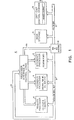
- FIG. 1 An illustrative desktop mainframe data processing system 10 is shown in FIG. 1.
- a primary processing unit 12 and its associated secondary microprocessor 14 are connected to a local processor bus 18.
- a floating point peripheral chip 16 for example an Intel 80287, is also connected to the processor bus 18.
- Local bus 18 is connected, in turn, by bus-to-bus adapter 20 to the system bus 22.
- Main storage 24 and the secondary control storage 26 are both connected to the system bus 22.
- the primary processor 12, secondary processor 14 and the floating point peripheral 16 are also responsively connected to processor control logic means 28 which incorporates processor control and interface logic and some private storage therefor. Certain aspects of the control logic means 28 shall be discussed hereinafter in greater detail.
- primary processor 12 is assigned the responsibility for performing all instruction fetches and operand address calculations for all of the processors used in the system. It also performs execution of all fixed point instructions, contains and maintains the general purpose registers, instruction length codes, condition codes and instruction addresses, recognizes system interrupts and provides indications to the system that a main storage instruction fetch or operand access is required. In addition, primary processor 12 is also able to provide an indication to the system that a change in processor control is needed.
- Secondary processor 14 performs execution of all system control instructions and maintains all of the control registers. When necessary, it performs the service processor function and provides indications to the system of main storage operand access and private storage microcode access. In addition, secondary microprocessor 14 is able to provide the system with an indication that a change in processor control is needed.
- Floating point peripheral chip 16 performs execution of all floating point instructions, containing and maintaining all of the floating point registers. It also provides the system with an indication of main storage operand access and of a need to alter microprocessor control. Alternatively, these floating point functions can be provided by a microprocessor rather than by a peripheral unit.
- Che mainframe instruction set is thus allocated for execution among the several processors.
- Primary processor 12 is provided with limited on-chip control store that can be utilized to store mainframe instruction responsive microcode and/or microprocessor interface and control microcode.
- on-chip control store that can be utilized to store mainframe instruction responsive microcode and/or microprocessor interface and control microcode.
- a main storage module 24 is attached to system bus 22 and used as needed by processors 12 and 14. It is assumed that the processor local bus 18 and microprocessors 12 and 14 all include 24 bits of addressing to accommodate the addressing structure of the mainframe to be implemented. It may be necessary to slightly modify currently available microprocessors to achieve this addressing capability.
- the secondary processor 14 uses off-chip control storage module 26, as may be necessary, for its own microcode and scratchpad functions. Processors 12 and 14, floating point peripheral 16 and processor control logic means 28 are interconnected together by and pass information to each other on the processor local bus 18.
- the microcode required by primary processor 12 and resident in its on-chip control store includes the microcode for primary processor memory accesses and related instruction decoding and execution.
- the microcode required by secondary microprocessor 14 resides in control storage 26 and is accessed via the system bus.
- main storage and control storage are a physically contiguous block of random access memory (RAM), with an exception to be discussed below.
- the dividing line between storage modules, as described herein, is the dividing line between real main storage and control storage.
- the main storage module 24 runs from address 00000 to address 77FFF (hexadecimal - hereinafter hex).
- the control storage module 26 runs from address 78000 to address 7FFFF (hex).
- the addresses used herein have been selected to simplify and facilitate this description. Those having skill in this art will recognize that the address limits for each memory module are a design choice and that the manipulation of more than one address bit, to steer between main and control storage, may be necessary.
- Private store 30, referred to previously, is logically a portion of off-chip control storage 26, but is physically located in the processor control logic means 28 and mapped into a reserved segment of control store 26.
- the reserved segment of control store 26 is typically about 256 bytes long, although it can be greater.
- Private store 30 includes one unique memory mapped address for each peripheral connected to the system bus. An access of any one of these peripheral addresses will invoke a bus cycle alteration when needed to provide the required synchronization.
- the processor control logic means 28 is connected to bus-to-bus interface 20 via bus feeder 18a. Also physically located in the processor control logic means 28 are a pair of override latches (not shown) that serve to steer memory accesses from processors 12 and 14 to either the main memory storage module 24 or to the off-chip control storage module 26, as is explained in greater detail in EP application 84109396.6.
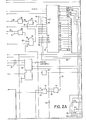
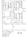
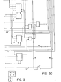
- FIG. 2 Data transfer to and from the memory mapped peripherals of the present system is handled in accordance with the apparatus shown in FIG. 2 and via the methodology explained hereinafter.
- the FIG. 2 apparatus is invoked after primary microprocessor 12 has received and decoded an instruction requiring use of a peripheral.
- This approach to data transfer contemplates that a peripheral to be serviced can be tightly coupled to the data bus and appropriately conditioned to timely write data to or read data from bus 18 without intermediate storage in the primary processor.
- that peripheral is assumed to be the floating point chip 16.
- the normal status ot a logic signal will be parenthetically indicated near the line carrying a particular signal.
- a logically low signal will be indicated as (L) and a logically high signal will be indicated as (H).
- Primary processor 12 When a floating point instruction is encountered by primary processor 12, it initiates action to utilize that peripheral.
- Primary processor 12 performs the tirst step in that procedure by forwarding a command to the peripheral. Since all peripherals in the present system are memory mapped, primary processor 12 sends a command, appropriate to the decoded instruction being executed, by attempting to "write" the appropriate command to the predetermined memory mapped location associated with peripheral 16, in this instance an address in the 5F2X (hex) range. Depending upon the nature of the floating point instruction being executed, primary processor 12 will either send a "write” or a "read” command to peripheral 16.
- a special decode or tunction code is responsively placed on certain of the primary processcr's output pins to signify that this instruction is one that will be taking its data directly from or sending it directly to main memory 24.
- peripheral 16 For purposes of clarity, it should be understood that if any peripneral i requires data, that data is written to the peripheral by first reading it from memory. Thus, if peripheral 16 needs data, it must be conditioned to have that data written to it. Similarly, if peripheral 16 has finished manipulating data, the results are read from the peripheral and then written to memory. It will first be assumed that the instruction being executed requires peripheral 16 to perform an operation that will need data from main memory.
- primary processor 12 writes a "write” :ommand to peripheral 16 and thereby to its associated memory mapped iddress, in this instance an address in the 5F2X (hex) range.
- the "X" signifies that the address can be completed by any hexadecimal value.
- the function code output pins of primary processor 12 and signal lines 38 connected thereto are conditioned to logically reflect the mature of the particular instruction being executed.
- the function code is read by decoder 40 which responsively sets its Y3 output to a logical low whenever a floating point command is detected. This logical low signal is Lnverted by inverter 42 and applied to one input of OR gate 44.
- a Function code indication of a command holds one input to OR gate 44 at a Logical high.
- rhe writing of a command to the memory mapped address associated with peripheral 16 causes that address to be placed on bus 18 from where it is received and detected by address decoder 50. Its Y2 output is set to a logical low whenever a write to the 5F2X (hex) address block is detected. That decoder 50 output is connected to the inverted input 52 of AND gate 54. Thus, whenever an access is attempted to the predetermined block of memory mapped locations associated with the system peripherals, input 52 of AND gate 54 is set to a logical high.
- the other input 56 of AND gate 54 is connected directly to the Al address line of bus 18, the penultimate least significant bit thereof. This address line is used, as shall be explained, to provide a toggle between commands and data.
- Al is logically low
- the input 56 of AND gate 54 is set logically high.
- output line 58 is set to a logical high, only when a memory mapped peripheral address is accessed and address bit Al is logically low. Under any other set of input conditions, output line 58 will be set at a logical low.
- OR gate 44 When output line 58 is at a logical high, OR gate 44 will be enabled. As previously described, when the appropriate function code is detected, the other input line to OR gate 44 will be set to a logical high. Thus, a logical high at either input of gate 44 will set its output to a logical high. However, both input lines of OR gate 44 must be at a logical low to force its output to a logical low.
- the output 46 of OR gate 44 is connected to the command/data inverted input pin 48 of floating point peripheral 16. When command/data pin 48 is set to a logical high, it causes peripheral 16 to be conditioned to accept or transfer data. When command/data pin 48 is set to a logical low, it causes peripheral 16 to look for command advice.
- peripheral 16 the next step is to advise the peripheral of the nature of the command.
- the control logic responds as follows. Detection of the appropriate function code caused by the primary processor 12 writing an appropriate command to 5F2X also sets the inverted input 60 of AND gate 62 to a logical high. Inverted input 64 of AND gate 62 is set to a logical high for a memory read, required for a peripheral "write", and to a logical low for a memory write, required to "read" from the peripheral.
- AND gate 68 The remaining inverted input 66 to AND gate 62 is conditioned by AND gate 68.
- AND gate 68 When both inputs are set to a logical high, AND gate 68 is enabled causing its inverted output to be set to a logical low. This causes inverted input 66 of AND gate 62 to be set to a logical high.
- Input 70 of AND gate 68 is set high to indicate that no error condition exists.
- Input 72 of AND gate 68 is set high to indicate that a System/370 memory access is to take place. When both of these conditions are satisfied, the output of AND gate 68 is enabled and then inverted to a logical low.
- AND gate 62 When all of its inputs are inverted to logical highs, AND gate 62 has its output line 76 set to a logical high. This puts one input of the floating point write OR gate 78 at a logical high. When input 76 of OR gate 78 is set to a logical high, its output 80 is enabled and inverted thereby to a logical low. This sets the write command pin 82 of floating point peripheral 16 and conditions it to accept the data it will need to perform its floating point function.
- the other input to OR gate 78 is also derived from a write to the memory mapped address associated with the floating point peripheral 16. It is provided for those instances where peripheral usage is required without invocation of a direct, single bus cycle, peripheral from memory data transfer.
- line 84 is set low. This signal is inverted by inverter 86 to a logical high whenever peripheral 16 is not busy. With output 88 of this invertfr set to a logical high, the other input to floating point write enable OR gate 78 is set to a logical high.
- input 88 of OR gate 78 is set to a logical high, its output 80 is enabled and set thereby to a logical low by inversion. This sets the write command pin 82 of floating point peripheral 16 and conditions it to accept the data it will need to perform its floating point function.
- peripheral 16 signals that it is ready by raising its ready line. This will eventually permit the start of a new bus cycle whereupon the primary processor will read the data needed by the peripheral 16 onto the data bus 22 from main memory 24. When that occurs, the data is forwarded to peripheral 16 by the bi-directional buffers 90 and 92, which are connected to the data bus. Buffers 90 and 92 are normally conditioned to pass data, in this embodiment, toward the peripheral being accessed.
- primary processor 12 Prior to a data read from main memory 24 and the appearance of data on the data bus 22, primary processor 12 sets address Al bit to a logical high. This causes input 58 to OR gate 44 to be set to a logical low. At the same time, the function code changes to indicate a data write and not a command write, which brings output Y3 of decoder 40 to a logical high. This also sets the other input of OR gate 44 to a logical low. With both inputs low, OR gate 44 has its output held low and the command/data input pin 48 of peripheral 16 is set high, thereby indicating data is to be transferred. This conditions peripheral 16 to have the data written to it directly from the bus 22 and bidirectional buffers 90 and 92 without it first having to be read into and out of the internal registers of primary processor 12.
- a peripheral read when manipulated data is to be transferred from the accessed peripheral to memory 24 is command conditioned in the same manner as was the peripheral write.
- primary processor 12 then initiates a peripheral "read" operation as follows.
- AND gate 96 is provided with three inverted inputs 98, 100 and 102.
- Input 98 is connected by signal line 104 to receive an address strobe signal that is active low.
- Input 100 is connected to receive the inverted output 106 of AND gate 108.
- Input 102 is connected to reflect the type of main memory access to be performed by signal line 110.
- the inputs 112 and 114 to AND gate 108 respectively reflect an address boundary error condition and a special function code detection from the output of inverter 42. Without said error and when the proper function code has been detected, AND gate 108 will be enabled setting its inverted output to a logical low and input pin 100 of AND gate 96 to a logical high. Similarly, a main memory write sets signal line 110 logically low and input 102 to a logical high. When the proper address strobe, active low, is received, AND gate 96 is enabled setting its output to a logical high.
- gate 118 has its output 120 set by inversion to a logical low.
- Output 120 of read enable gate 118 is connected to the read pin 122 of peripheral 16. When set high, this pin conditions the peripheral to have data read therefrom.
- Output 120 of read enable gate 118 is also connected to the directional control pins 124 of the bidirectional buffers 90 and 92. When set high, these pins force the buffers to transfer data from the peripheral to the data bus 22.
- output 120 will be at a logical high which sets the directional control pins 124 of buffers 90 and 92 to transfer data from bus 22 to the peripheral.
- the other input 126 to OR gate 118 is also derived from a write to the memory mapped address associated with the floating point peripheral 16. It is provided for those instances where peripheral usage is required without invocation of a direct, single bus cycle peripheral to memory data transfer.
- line 128 is set low. This signal is inverted by inverter 130 to a logical high whenever peripheral 16 is not busy. With output of inverter 130 set to a logical high, input 126 to floating point read enable OR gate 118 is set to a logical high.
- input 126 of OR gate 118 is set to a logical high, its output 120 is enabled and inverted thereby to a logical low. This sets the read command pin 122 of floating point peripheral 16 and conditions it to issue the data it will need to deliver in performing its floating point function.
Landscapes
- Engineering & Computer Science (AREA)
- Theoretical Computer Science (AREA)
- Software Systems (AREA)
- Physics & Mathematics (AREA)
- General Engineering & Computer Science (AREA)
- General Physics & Mathematics (AREA)
- Multi Processors (AREA)
- Information Transfer Systems (AREA)
- Bus Control (AREA)
Applications Claiming Priority (2)
| Application Number | Priority Date | Filing Date | Title |
|---|---|---|---|
| US54293583A | 1983-10-18 | 1983-10-18 | |
| US542935 | 1983-10-18 |
Publications (2)
| Publication Number | Publication Date |
|---|---|
| EP0139254A2 true EP0139254A2 (de) | 1985-05-02 |
| EP0139254A3 EP0139254A3 (de) | 1988-06-08 |
Family
ID=24165901
Family Applications (1)
| Application Number | Title | Priority Date | Filing Date |
|---|---|---|---|
| EP84111589A Ceased EP0139254A3 (de) | 1983-10-18 | 1984-09-28 | Vorrichtung und Verfahren für direkte Datenübertragung vom Speicher an das Peripheriegerät und vom Peripheriegerät an den Speicher |
Country Status (3)
| Country | Link |
|---|---|
| EP (1) | EP0139254A3 (de) |
| JP (1) | JPS6097458A (de) |
| CA (1) | CA1208802A (de) |
Cited By (12)
| Publication number | Priority date | Publication date | Assignee | Title |
|---|---|---|---|---|
| EP0261685A3 (de) * | 1986-09-24 | 1991-04-24 | Hitachi, Ltd. | Mikroprozessorsystem |
| EP0318702A3 (de) * | 1987-10-30 | 1992-04-01 | Hitachi, Ltd. | Datenprozessor mit direktem Datentransfer zwischen Koprozessor und Speicher |
| US5193159A (en) * | 1986-09-24 | 1993-03-09 | Hitachi, Ltd. | Microprocessor system |
| WO1998055932A3 (en) * | 1997-06-04 | 1999-08-12 | Richard Rubinstein | Processor interfacing to memory mapped computing engine |
| WO2000022546A3 (en) * | 1998-10-14 | 2000-07-20 | Triscend Corp | Configurable processor system unit |
| US6691206B1 (en) | 1997-03-21 | 2004-02-10 | Marger Johnson & Mccollom, P.C. | Processor interfacing to memory-centric computing engine |
| US6704850B1 (en) | 2000-08-23 | 2004-03-09 | Triscend Corporation | Method and apparatus for determining the width of a memory subsystem |
| US6721840B1 (en) | 2000-08-18 | 2004-04-13 | Triscend Corporation | Method and system for interfacing an integrated circuit to synchronous dynamic memory and static memory |
| EP0752666A3 (de) * | 1995-07-06 | 2004-04-28 | Sun Microsystems, Inc. | Verfahren und Vorrichtung zur Beschleunigung von Sklave-Anforderungen in einem paketvermittelten Computersystem |
| US6895452B1 (en) | 1997-06-04 | 2005-05-17 | Marger Johnson & Mccollom, P.C. | Tightly coupled and scalable memory and execution unit architecture |
| US6920551B1 (en) | 2001-03-08 | 2005-07-19 | Xilinx, Inc. | Configurable processor system |
| US8504808B2 (en) | 2002-08-07 | 2013-08-06 | Mmagix Technology Limited | Cache memory apparatus having internal ALU |
Families Citing this family (1)
| Publication number | Priority date | Publication date | Assignee | Title |
|---|---|---|---|---|
| JPS60195661A (ja) * | 1984-03-19 | 1985-10-04 | Hitachi Ltd | デ−タ処理システム |
Family Cites Families (4)
| Publication number | Priority date | Publication date | Assignee | Title |
|---|---|---|---|---|
| US4270167A (en) * | 1978-06-30 | 1981-05-26 | Intel Corporation | Apparatus and method for cooperative and concurrent coprocessing of digital information |
| US4249240A (en) * | 1979-03-02 | 1981-02-03 | Xycom, Inc. | Address system for bus interconnected computer system |
| JPS5840214B2 (ja) * | 1979-06-26 | 1983-09-03 | 株式会社東芝 | 計算機システム |
| JPS56116138A (en) * | 1980-02-15 | 1981-09-11 | Omron Tateisi Electronics Co | Input and output controller |
-
1984
- 1984-08-18 JP JP17102084A patent/JPS6097458A/ja active Granted
- 1984-09-11 CA CA000462900A patent/CA1208802A/en not_active Expired
- 1984-09-28 EP EP84111589A patent/EP0139254A3/de not_active Ceased
Cited By (16)
| Publication number | Priority date | Publication date | Assignee | Title |
|---|---|---|---|---|
| US5193159A (en) * | 1986-09-24 | 1993-03-09 | Hitachi, Ltd. | Microprocessor system |
| EP0261685A3 (de) * | 1986-09-24 | 1991-04-24 | Hitachi, Ltd. | Mikroprozessorsystem |
| EP0318702A3 (de) * | 1987-10-30 | 1992-04-01 | Hitachi, Ltd. | Datenprozessor mit direktem Datentransfer zwischen Koprozessor und Speicher |
| EP0752666A3 (de) * | 1995-07-06 | 2004-04-28 | Sun Microsystems, Inc. | Verfahren und Vorrichtung zur Beschleunigung von Sklave-Anforderungen in einem paketvermittelten Computersystem |
| US6691206B1 (en) | 1997-03-21 | 2004-02-10 | Marger Johnson & Mccollom, P.C. | Processor interfacing to memory-centric computing engine |
| US6895452B1 (en) | 1997-06-04 | 2005-05-17 | Marger Johnson & Mccollom, P.C. | Tightly coupled and scalable memory and execution unit architecture |
| WO1998055932A3 (en) * | 1997-06-04 | 1999-08-12 | Richard Rubinstein | Processor interfacing to memory mapped computing engine |
| US6467009B1 (en) | 1998-10-14 | 2002-10-15 | Triscend Corporation | Configurable processor system unit |
| GB2361559B (en) * | 1998-10-14 | 2003-08-27 | Triscend Corp | Configurable processor system unit |
| GB2361559A (en) * | 1998-10-14 | 2001-10-24 | Triscend Corp | Configurable processor system unit |
| WO2000022546A3 (en) * | 1998-10-14 | 2000-07-20 | Triscend Corp | Configurable processor system unit |
| US6721840B1 (en) | 2000-08-18 | 2004-04-13 | Triscend Corporation | Method and system for interfacing an integrated circuit to synchronous dynamic memory and static memory |
| US6704850B1 (en) | 2000-08-23 | 2004-03-09 | Triscend Corporation | Method and apparatus for determining the width of a memory subsystem |
| US6920551B1 (en) | 2001-03-08 | 2005-07-19 | Xilinx, Inc. | Configurable processor system |
| US8504808B2 (en) | 2002-08-07 | 2013-08-06 | Mmagix Technology Limited | Cache memory apparatus having internal ALU |
| US9274969B2 (en) | 2002-08-07 | 2016-03-01 | Mmagix Technology Limited | Cache memory apparatus |
Also Published As
| Publication number | Publication date |
|---|---|
| JPH0316660B2 (de) | 1991-03-06 |
| JPS6097458A (ja) | 1985-05-31 |
| EP0139254A3 (de) | 1988-06-08 |
| CA1208802A (en) | 1986-07-29 |
Similar Documents
| Publication | Publication Date | Title |
|---|---|---|
| US4942519A (en) | Coprocessor having a slave processor capable of checking address mapping | |
| US5664199A (en) | Microcomputer free from control of central processing unit (CPU) for receiving and writing instructions into memory independent of and during execution of CPU | |
| US4716527A (en) | Bus converter | |
| US5706514A (en) | Distributed execution of mode mismatched commands in multiprocessor computer systems | |
| US3996564A (en) | Input/output port control | |
| EP0135753A2 (de) | Vorrichtung zur Annullierung einer Speicherwahl in einem mit einem Mikroprozessor versehenen Datenverarbeitungssystem | |
| US5014236A (en) | Input/output bus expansion interface | |
| US4731736A (en) | Method and apparatus for coordinating execution of an instruction by a selected coprocessor | |
| US4750110A (en) | Method and apparatus for executing an instruction contingent upon a condition present in another data processor | |
| US5146605A (en) | Direct control facility for multiprocessor network | |
| EP0437550B1 (de) | Verfahren und vorrichtung zur emulation eines informationsverarbeitungssystems | |
| US7007126B2 (en) | Accessing a primary bus messaging unit from a secondary bus through a PCI bridge | |
| CA1208802A (en) | Apparatus and method for direct memory to peripheral and peripheral to memory data transfers | |
| US4972317A (en) | Microprocessor implemented data processing system capable of emulating execution of special instructions not within the established microprocessor instruction set by switching access from a main store portion of a memory | |
| EP0525831B1 (de) | Verfahren und Vorrichtung für ein Processor um mit einem Coprocessor in der Verarbeitung eines im Programablauf des Processors befindlichen Befehls mitzuwirken. | |
| US4628445A (en) | Apparatus and method for synchronization of peripheral devices via bus cycle alteration in a microprocessor implemented data processing system | |
| US4758950A (en) | Method and apparatus for selectively delaying an interrupt of a coprocessor | |
| US4914578A (en) | Method and apparatus for interrupting a coprocessor | |
| JPH0232659B2 (de) | ||
| US5003468A (en) | Guest machine execution control system for virutal machine system | |
| US5933613A (en) | Computer system and inter-bus control circuit | |
| US4814977A (en) | Apparatus and method for direct memory to peripheral and peripheral to memory data transfers | |
| US4758978A (en) | Method and apparatus for selectively evaluating an effective address for a coprocessor | |
| EP0138045A2 (de) | Vorrichtung und Verfahren für die Synchronisation von Peripheriegeräten mittels Änderung von Buszyklen in einem Mikroprozessor-Datenverarbeitungssystem | |
| US5734900A (en) | Information handling system including efficient power on initialization |
Legal Events
| Date | Code | Title | Description |
|---|---|---|---|
| PUAI | Public reference made under article 153(3) epc to a published international application that has entered the european phase |
Free format text: ORIGINAL CODE: 0009012 |
|
| 17P | Request for examination filed |
Effective date: 19841123 |
|
| AK | Designated contracting states |
Designated state(s): DE FR GB |
|
| PUAL | Search report despatched |
Free format text: ORIGINAL CODE: 0009013 |
|
| AK | Designated contracting states |
Kind code of ref document: A3 Designated state(s): DE FR GB |
|
| 17Q | First examination report despatched |
Effective date: 19890915 |
|
| STAA | Information on the status of an ep patent application or granted ep patent |
Free format text: STATUS: THE APPLICATION HAS BEEN REFUSED |
|
| 18R | Application refused |
Effective date: 19910921 |
|
| APAF | Appeal reference modified |
Free format text: ORIGINAL CODE: EPIDOSCREFNE |
|
| RIN1 | Information on inventor provided before grant (corrected) |
Inventor name: BUONOMO, JOSEPH P. Inventor name: OLIVER, BURTON L. Inventor name: LOSINGER, RAYMOND E. |