EP0140042A2 - Digitale Phasenriegelschleife - Google Patents
Digitale Phasenriegelschleife Download PDFInfo
- Publication number
- EP0140042A2 EP0140042A2 EP84110506A EP84110506A EP0140042A2 EP 0140042 A2 EP0140042 A2 EP 0140042A2 EP 84110506 A EP84110506 A EP 84110506A EP 84110506 A EP84110506 A EP 84110506A EP 0140042 A2 EP0140042 A2 EP 0140042A2
- Authority
- EP
- European Patent Office
- Prior art keywords
- pulse
- reference clock
- waveform
- clock
- signal
- Prior art date
- Legal status (The legal status is an assumption and is not a legal conclusion. Google has not performed a legal analysis and makes no representation as to the accuracy of the status listed.)
- Granted
Links
- 230000003111 delayed effect Effects 0.000 claims abstract description 13
- 238000007493 shaping process Methods 0.000 claims abstract description 9
- 230000004044 response Effects 0.000 claims description 7
- 230000003247 decreasing effect Effects 0.000 claims description 3
- 238000001514 detection method Methods 0.000 claims 2
- 238000010586 diagram Methods 0.000 description 5
- 230000010363 phase shift Effects 0.000 description 3
- 230000000630 rising effect Effects 0.000 description 3
- 230000009471 action Effects 0.000 description 2
- 230000001360 synchronised effect Effects 0.000 description 2
- 230000008859 change Effects 0.000 description 1
- 230000003993 interaction Effects 0.000 description 1
- 238000012986 modification Methods 0.000 description 1
- 230000004048 modification Effects 0.000 description 1
- 230000001172 regenerating effect Effects 0.000 description 1
- 230000000979 retarding effect Effects 0.000 description 1
- 238000000926 separation method Methods 0.000 description 1
- 230000007704 transition Effects 0.000 description 1
Images


Classifications
-
- H—ELECTRICITY
- H03—ELECTRONIC CIRCUITRY
- H03L—AUTOMATIC CONTROL, STARTING, SYNCHRONISATION OR STABILISATION OF GENERATORS OF ELECTRONIC OSCILLATIONS OR PULSES
- H03L7/00—Automatic control of frequency or phase; Synchronisation
- H03L7/06—Automatic control of frequency or phase; Synchronisation using a reference signal applied to a frequency- or phase-locked loop
- H03L7/08—Details of the phase-locked loop
- H03L7/081—Details of the phase-locked loop provided with an additional controlled phase shifter
- H03L7/0812—Details of the phase-locked loop provided with an additional controlled phase shifter and where no voltage or current controlled oscillator is used
- H03L7/0814—Details of the phase-locked loop provided with an additional controlled phase shifter and where no voltage or current controlled oscillator is used the phase shifting device being digitally controlled
-
- H—ELECTRICITY
- H04—ELECTRIC COMMUNICATION TECHNIQUE
- H04L—TRANSMISSION OF DIGITAL INFORMATION, e.g. TELEGRAPHIC COMMUNICATION
- H04L7/00—Arrangements for synchronising receiver with transmitter
- H04L7/02—Speed or phase control by the received code signals, the signals containing no special synchronisation information
- H04L7/033—Speed or phase control by the received code signals, the signals containing no special synchronisation information using the transitions of the received signal to control the phase of the synchronising-signal-generating means, e.g. using a phase-locked loop
- H04L7/0337—Selecting between two or more discretely delayed clocks or selecting between two or more discretely delayed received code signals
Definitions
- the present invention relates to a digital phase lock loop (PLL) circuit operable at high speed and, more particularly, to a digital PLL circuit for use in a hard disk drive.
- PLL digital phase lock loop
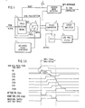
- a typical PLL circuit of this type would include a sync field detector 1, a reference oscillator 2, a phase comparator 3, an error amplifier 4, a low pass filter 5, a voltage controlled oscillator (VCO) 6, and an address mark detector 7.
- the VCO generates a clock pulse having a frequency and phase synchronized with the data.
- the comparator generates pulses corresponding to the difference in the relative position of the data and the VCO timing clock pulse. The output of the comparator represents the "error signal" for controlling the PLL loop.
- the error amplifier converts the TTL (transistor-transistor logic) pulses from the phase comparator into constant current pulses and isolates any logic noise that might be present in the phase comparator outputs.
- the low pass filter arranged between the error amplifier and the VCO serves to reject certain frequency components while passing others, so that the high frequency jitter caused by various magnetic recording phenomena can be averaged or rejected.
- the sync field detector prevents the VCO from slewing to a high frequency and being locked to a harmonic of the basic read/write frequency for the disk data. More specifically, when data is written to a disk there are areas on the disk that will contain invalid high frequency bursts, or "write glitches" due to a WRITE GATE being asserted and negated, data being recorded with a slightly different phase, a write current of an improper value at the beginning or end of the WRITE GATE, or for some other reason.
- the VCO may be caused to slew to a high frequency and the VCO may then become locked to a higher harmonic when the normal data subsequently returns.
- the sync field detector 1 first maintains the VCO frequency locked to a desired frequency by passing a reference signal of predetermined frequency from the reference clock generator 2, e.g., 10 MHz, to the phase comparator 3, and the data is only provided to the phase comparator 3 after a sync field is detected.
- a sync field is provided in the form of an all-zero pattern of a predetermined number of bits recorded in front of each of the ID FIELD and the DATA FIELD and an address mark is recorded after each sync field but before the ID field or data field .
- the switch 9 will be changed to select the reproduced data for provision to the phase comparator 3.
- the address mark detector 7 then examines the output of the switch 9 and provides a reset signal to the field detecting means 8 if an address mark is not detected within some predetermined period of time. The search for the sync field will then begin over again.
- the reproduced data continues to be selected for a predetermined period of time long enough to detect the ID or data information. In this way, the reproduced data is not selected to control the PLL during the gap periods between 'fields when the WRITE GATE is turned on and off.
- An object of the invention is to provide a novel, simplified digital PLL circuit free from the above-mentioned various disadvantages in the conventional analog PLL circuit.
- a digital PLL circuit comprising a reference clock pulse generator whose clock frequency is higher than the rate of raw data pulses received from an external device; a pulse shaper for subjecting each of said data pulses to waveform-shaping to obtain waveform-shaped pulses having pulse widths approximately equal to one clock period of said reference clock pulses; means for producing a phase control pulse on the basis of the relative positions of a delayed reference clock pulse and each of said waveform-shaped data pulses; and means for generating said delayed reference clock pulse in response to said phase control pulse.
- the pulse-shaping device generates two pulses in addition to the waveform-shaped data.
- a first pulse has a duration covering approximately the first 30 percent of the data period, and a second pulse covers approximately the last 30 percent of the data period.
- the clock timing is considered to be correct and no action is taken.
- a delay or advance signal is generated, as appropriate, and the generated delay or advance signal is provided to an up/down counter. The counter value then changes accordingly, and the counter output is used to select from a number of phase-delayed versions of the clock signal, with the selected clock signal being provided as the phase-corrected clock signal.
- one embodiment of the invention comprises a reference clock generator 10 whose clock frequency of, e.g.,. 10 MHz is selected to be twice the 5 MHz rate of raw data pulses reproduced from a disc drive (not shown), a pulse shaper 20 for subjecting the reproduced data pulses to waveform-shaping, a phase comparator 30 for producing a phase control pulse on the basis of the relative position of a correspondingly delayed reference clock (VCLK) pulse with respect to each of said waveform-shaped data pulses from the shaper 20, and a phase shifter 40 for generating said VCLK pulse in response to said phase control pulse.
- VCLK correspondingly delayed reference clock
- the pulse shaper 20 includes a D-type flip-flop 21; a delay line circuit 22 for providing a total of 100 nanoseconds delay selectable in 10 ns increments through 10 taps (T10, T20,...,T100); inverters 23, 24, and 25, each of which has a gate delay; AND gates 26 and 27; and OR gate 28.
- Each circle marked at the input or output of the flip-flop, inverters and AND gates represents an inversion of a given input or output.
- UP ENB UP ENB
- DOWN ENB waveform-shaped data
- D0, D50, D30, D40, D50, D70 and D100 indicate outputs appearing at corresponding signal lines shown in Fig. 2.
- the UP ENB signal is obtained as the inversion of a logical product (DO ⁇ D30) whose pulse width is equal to, e.g., 30 percent of one reference clock period (CP) of 100 nanoseconds, assuming a low level during approximately the first 30 percent of the waveform-shaped data from the OR gate 28.
- DOWN ENB is the inversion of a logical product (D70'D100) having a pulse width equal to 30 percent of one CP and assumes a low level during approximately the last 30 percent of the data from the gate 28.
- the waveform-shaped data having a pulse width substantially equal to one CP is generated as a logical sum (D10 + D40) at the gate 28.
- the digital phase comparator 30 includes two D-type flip-flops 31 and 32 for detecting the occurrence of the rising edge of the above-mentioned VCLK pulse during the low level period of either the UP ENB or DOWN ENB signals from the shaper 20, and a D-type flip-flop 33 for producing normalized data to be provided to a disk controller (not shown) which controls the data writing-in and reading-out operations for the disk drive and also communicates with a host computer (not shown).
- the timing relationship ensures that there will be only one of the flip-flops 31 and 32 set (i.e., have a low level Q output) at any given time.
- the flip-flop 33 is always set in response to the waveform-shaped data from the gate 28.
- Each of the three flip-flops 31 to 33 is set for one VCLK period, because the next rising edge of the VCLK pulse will clear it.
- the phase shifter 40 is constructed of a delay line circuit 41, a multiplexer 42 and an up/down counter 43.
- the delay line circuit 41 provides a total 100-nanosecond delay with 10 taps (T1,T2,..., T9,T10), each of which provides a relative delay increment of ten percent of the total delay, with the total delay being equal to the reference clock period.
- the up/down counter 43 generates a binary selection address to the multiplexer 42 so that one out of the ten taps of the delay line circuit 41 is selected to produce a reference clock pulse with the phase shifted correspondingly.
- the center 43 may be a conventional LS192 ring counter and will increment or decrement each time a positive-going transition occurs in the UP or DOWN signals, respectively.
- the up/down counter 43 Each time the up/down counter 43 is incremented or decremented by the UP or DOWN signal from the flip-flop 31 or 32, an output signal different in phase by ten percent from the present phase angle is produced as a new VCLK pulse from the multiplexer 42. Consequently, the counter 43 has a 360° digital phase shift function in digital 10 percent increments.
- the counter 43 preferably has a maximum value of 9, starting from 0 and returning to 0 after it has reached 9.
- the multiplexer may be a 74150 multiplexer which selects one of the taps T1-T10 - in accordance with the value on lines 43-1 through 43-4, but selects the signal on any one of lines 42-1 through 42-6 whenever the value in counter 43 exceeds its allowable maximum value of, e.g., "9".
- the relationship between the taps of the delay line circuit 41 which are selected, the values of the counter 43 and UP and DOWN signals from the flip-flops 31 and 32 can be more clearly understood by referring to the following Table which illustrates one hypothetical sequence of clock shifts.
- a VCLK pulse Vl appears early with respect to raw data 1 from a hard disk drive (not shown)
- the leading edge of the pulse Vl is detected by the flip-flop 31 during the low level period Ll of the signal UP ENB from the shaper 20.
- a low level UP signal L2 is produced from the flip-flop 31 in synchronism with the rising edge of the pulse VI and having a duration of one VCLK period P1 equal to t 1 + t 2 .
- the leading edge of a VCLK pulse V2 With the leading edge of a VCLK pulse V2, the low level UP signal L2 becomes a high level Hl.
- the second half of the clock cycle is illustrated as being elongated in the waveform VCLK of Fig. 3B. This is" due to the propagation time of the leading edge of the clock pulse VCLK from the output of multiplexer 42 through the flip-flops 31, 32 and counter 43 and the response time of multiplexer 42 to a change in the counter value.
- This propagation delay is typically greater than 50 nanoseconds, i.e., larger than the first half cycle of the signal VCLK.
- the present invention allows phase timing correction in digital form to overcome the above-mentioned disadvantages inherent in the prior art analog PLL circuit shown in Fig. 1.
- Parts of the system other than the flip-flop 21 of the pulse shaper 20 may be replaced by the circuit shown in Fig 4A.
- the timing relationship among the 0 ENB, DOWN ENB and waveform-shaped data is illustrated in Fig. 4B.
- a reset terminal 43-5 of the counter 43 is grounded so as not to stop the operation of the counter 43.
- each of the terminals 42-1...42-6 of the multiplexer 42 is used to receive an input reference clock from the generator 10 directly without providing any delay.
- any one of the terminals 42-1...42-6 can be used to provide an undelayed clock signal when the value of the counter 43 erroneously takes a value larger than 9. For example, if on power-up the counter 43 erroneously assumes a value greater than "9", the counter value must be decreased to return the system to stable operation. Accordingly, the undelayed clock signal is selected as VCLK and this will result in a continuous stream of UP or DOWN signals to the counter 43 until the count value returns to its permitted range.
Landscapes
- Stabilization Of Oscillater, Synchronisation, Frequency Synthesizers (AREA)
- Signal Processing For Digital Recording And Reproducing (AREA)
Applications Claiming Priority (2)
| Application Number | Priority Date | Filing Date | Title |
|---|---|---|---|
| US534058 | 1983-09-20 | ||
| US06/534,058 US4617679A (en) | 1983-09-20 | 1983-09-20 | Digital phase lock loop circuit |
Publications (3)
| Publication Number | Publication Date |
|---|---|
| EP0140042A2 true EP0140042A2 (de) | 1985-05-08 |
| EP0140042A3 EP0140042A3 (en) | 1986-08-27 |
| EP0140042B1 EP0140042B1 (de) | 1990-12-12 |
Family
ID=24128550
Family Applications (1)
| Application Number | Title | Priority Date | Filing Date |
|---|---|---|---|
| EP84110506A Expired - Lifetime EP0140042B1 (de) | 1983-09-20 | 1984-09-04 | Digitale Phasenriegelschleife |
Country Status (4)
| Country | Link |
|---|---|
| US (1) | US4617679A (de) |
| EP (1) | EP0140042B1 (de) |
| JP (1) | JPS60126921A (de) |
| DE (1) | DE3483742D1 (de) |
Cited By (8)
| Publication number | Priority date | Publication date | Assignee | Title |
|---|---|---|---|---|
| EP0240232A3 (de) * | 1986-04-01 | 1988-11-17 | Hewlett-Packard Company | Digitale Phasenregelschleife |
| EP0360349A3 (de) * | 1988-09-22 | 1990-11-22 | Philips Patentverwaltung GmbH | Digitaler Frequenzgenerator |
| DE3931259A1 (de) * | 1989-09-19 | 1991-03-28 | Siemens Ag | Verfahren zur fortlaufenden anpassung der phase eines digitalsignals an einen takt |
| EP0398174A3 (de) * | 1989-05-19 | 1991-09-04 | National Semiconductor Corporation | Verfahren eingebauter Fensterabtastung für einen Datensynchronisierer |
| WO1995019067A1 (en) * | 1994-01-04 | 1995-07-13 | Level One Communications, Inc. | A digitally controlled first order jitter attenuator using a digital frequency synthesizer |
| RU2119717C1 (ru) * | 1997-04-15 | 1998-09-27 | Пензенский технологический институт | Устройство фазовой синхронизации |
| GB2348327A (en) * | 1999-02-18 | 2000-09-27 | Sgs Thomson Microelectronics | Clock skew removal apparatus |
| EP3142287A1 (de) * | 2015-09-09 | 2017-03-15 | Imagination Technologies Limited | Synchronisationsvorrichtungen |
Families Citing this family (45)
| Publication number | Priority date | Publication date | Assignee | Title |
|---|---|---|---|---|
| DE3685616T2 (de) * | 1985-07-09 | 1993-02-04 | Nippon Electric Co | Phasenverriegelte taktregenerierschaltung fuer digitale uebertragungssysteme. |
| US4740997A (en) * | 1985-08-05 | 1988-04-26 | Hayes Microcomputer Products, Inc. | Band clock offset phase locked loop |
| US4715000A (en) * | 1985-08-06 | 1987-12-22 | General Electric Company | Digital phase-locked loop and frequency measuring device |
| BE904101A (nl) * | 1986-01-24 | 1986-07-24 | Bell Telephone Mfg Cy | Beeldverwerkingssysteem en daarin toegepaste fazevergrendelingslus. |
| JPS63214618A (ja) * | 1987-03-03 | 1988-09-07 | Yamaha Corp | デジタル・フェイズ・ロックド・ル−プ |
| US4943857A (en) * | 1987-04-24 | 1990-07-24 | Hitachi, Ltd. | Synchronizing circuit for an external signal and an internal sampling clock signal |
| FR2617349B1 (fr) * | 1987-06-26 | 1989-10-20 | Thomson Csf | Procede et dispositif de synthese numerique d'un signal d'horloge |
| US4814879A (en) * | 1987-08-07 | 1989-03-21 | Rca Licensing Corporation | Signal phase alignment circuitry |
| US4791488A (en) * | 1987-08-12 | 1988-12-13 | Rca Licensing Corporation | Line-locked clock signal generation system |
| US4847870A (en) * | 1987-11-25 | 1989-07-11 | Siemens Transmission Systems, Inc. | High resolution digital phase-lock loop circuit |
| JP2656288B2 (ja) * | 1988-02-29 | 1997-09-24 | 株式会社東芝 | 位相検波回路 |
| US4975930A (en) * | 1988-11-02 | 1990-12-04 | Digital Equipment Corporation | Digital phase locked loop |
| DE3843262C2 (de) * | 1988-12-22 | 1994-04-28 | Ant Nachrichtentech | Verfahren und Schaltungsanordnung zum Regeln der Phasenlage eines Taktsignals |
| US5056118A (en) * | 1989-05-16 | 1991-10-08 | Rockwell International Corporation | Method and apparatus for clock and data recovery with high jitter tolerance |
| US4992874A (en) * | 1989-07-03 | 1991-02-12 | Rca Licensing Corporation | Method and apparatus for correcting timing errors as for a multi-picture display |
| US5047967A (en) * | 1989-07-19 | 1991-09-10 | Apple Computer, Inc. | Digital front end for time measurement and generation of electrical signals |
| JPH0396015A (ja) * | 1989-09-08 | 1991-04-22 | Oki Electric Ind Co Ltd | 高速デジタルpll装置 |
| US5022056A (en) * | 1989-10-23 | 1991-06-04 | National Semiconductor Corporation | Method and structure for digital phase synchronization |
| CA2001266C (en) * | 1989-10-23 | 1996-08-06 | John Robert Long | Digital phase aligner and method for its operation |
| US5036528A (en) * | 1990-01-29 | 1991-07-30 | Tandem Computers Incorporated | Self-calibrating clock synchronization system |
| US5118975A (en) * | 1990-03-05 | 1992-06-02 | Thinking Machines Corporation | Digital clock buffer circuit providing controllable delay |
| JPH0447194U (de) * | 1990-08-24 | 1992-04-22 | ||
| US5109394A (en) * | 1990-12-24 | 1992-04-28 | Ncr Corporation | All digital phase locked loop |
| US5455935A (en) * | 1991-05-31 | 1995-10-03 | Tandem Computers Incorporated | Clock synchronization system |
| US5271040A (en) * | 1991-12-20 | 1993-12-14 | Vlsi Technology, Inc. | Phase detector circuit |
| EP0640261A4 (en) * | 1992-05-14 | 1995-04-05 | Vlsi Technology, Inc. | Data transmission delaying circuit using time-multiplexed latch enable signals. |
| US5416806A (en) * | 1992-06-15 | 1995-05-16 | International Business Machines Corporation | Timing loop method and apparatus for PRML data detection |
| US5488641A (en) * | 1992-12-10 | 1996-01-30 | Northern Telecom Limited | Digital phase-locked loop circuit |
| JPH06197014A (ja) * | 1992-12-25 | 1994-07-15 | Mitsubishi Electric Corp | 位相同期回路 |
| US5546434A (en) * | 1995-05-16 | 1996-08-13 | Intel Corporation | Dual edge adjusting digital phase-locked loop having one-half reference clock jitter |
| US5646519A (en) * | 1995-06-07 | 1997-07-08 | Symmetricom, Inc. | Digital phase detector employing a digitally controllable delay line |
| EP0842578A4 (de) * | 1995-08-01 | 1998-12-09 | Auravision Corp | System zur synchronisation von videosignalen mit flankenphasenausrichtung |
| US6266381B1 (en) * | 1998-01-22 | 2001-07-24 | Lsi Logic Corporation | Frequency control arrangement |
| US6646964B1 (en) * | 2000-03-27 | 2003-11-11 | Hewlett-Packard Development Company, L.P. | Harmonic correction in phase-locked loops |
| US6351165B1 (en) * | 2000-08-21 | 2002-02-26 | Exar Corporation | Digital jitter attenuator using an accumulated count of phase differences |
| US7440511B2 (en) * | 2001-04-25 | 2008-10-21 | Texas Instruments Incorporated | Transmit filter |
| US6975695B1 (en) * | 2001-04-30 | 2005-12-13 | Cypress Semiconductor Corp. | Circuit for correction of differential signal path delays in a PLL |
| US7512202B2 (en) * | 2003-07-28 | 2009-03-31 | Analog Devices, Inc. | Harmonic detector system and method |
| US7198675B2 (en) | 2003-09-30 | 2007-04-03 | Advanced Cardiovascular Systems | Stent mandrel fixture and method for selectively coating surfaces of a stent |
| JP4198639B2 (ja) * | 2004-05-27 | 2008-12-17 | Necエレクトロニクス株式会社 | 割り込み発生回路 |
| US8116321B2 (en) * | 2004-06-16 | 2012-02-14 | Thomson Licensing | System and method for routing asynchronous signals |
| US7733588B1 (en) * | 2006-01-04 | 2010-06-08 | Marvell International Ltd. | Repetitive feed-forward algorithm for self-servo-write PLL |
| US8003156B2 (en) | 2006-05-04 | 2011-08-23 | Advanced Cardiovascular Systems, Inc. | Rotatable support elements for stents |
| US9106400B2 (en) * | 2012-10-23 | 2015-08-11 | Futurewei Technologies, Inc. | Hybrid timing recovery for burst mode receiver in passive optical networks |
| CN103986463B (zh) * | 2014-05-08 | 2017-02-01 | 无锡友达电子有限公司 | 一种收音机pll系统和载波锁相方法 |
Family Cites Families (14)
| Publication number | Priority date | Publication date | Assignee | Title |
|---|---|---|---|---|
| FR1277331A (fr) * | 1960-10-17 | 1961-12-01 | Central De Telecomm Sa Lab | Perfectionnements aux dispositifs de régénération d'impulsions |
| US3509471A (en) * | 1966-11-16 | 1970-04-28 | Communications Satellite Corp | Digital phase lock loop for bit timing recovery |
| FR2167259B1 (de) * | 1972-01-11 | 1976-06-11 | Thomson Csf | |
| FR2292380A1 (fr) * | 1974-11-25 | 1976-06-18 | Cit Alcatel | Dispositif numerique de reconnaissance d'un message nrz |
| US3961138A (en) * | 1974-12-18 | 1976-06-01 | North Electric Company | Asynchronous bit-serial data receiver |
| US4189622A (en) * | 1975-10-17 | 1980-02-19 | Ncr Corporation | Data communication system and bit-timing circuit |
| JPS585614B2 (ja) * | 1976-09-08 | 1983-02-01 | 日本電信電話株式会社 | 位相同期発振器 |
| JPS53126250A (en) * | 1977-04-11 | 1978-11-04 | Nec Corp | Digital phase synchronous system |
| US4151485A (en) * | 1977-11-21 | 1979-04-24 | Rockwell International Corporation | Digital clock recovery circuit |
| US4218771A (en) * | 1978-12-04 | 1980-08-19 | Rockwell International Corporation | Automatic clock positioning circuit for a digital data transmission system |
| DE2924922A1 (de) * | 1979-06-20 | 1981-01-22 | Siemens Ag | Verfahren und schaltungsanordnung zur taktsynchronisierung bei der uebertragung von digitalen nachrichtensignalen |
| JPS5635536A (en) * | 1979-08-30 | 1981-04-08 | Fujitsu Ltd | Digital phase synchronous circuit |
| NL183214C (nl) * | 1980-01-31 | 1988-08-16 | Philips Nv | Inrichting voor het synchroniseren van de fase van een lokaal opgewekt kloksignaal met de fase van een ingangssignaal. |
| JPS5894241A (ja) * | 1981-11-30 | 1983-06-04 | Nec Home Electronics Ltd | クロックパルス発生回路 |
-
1983
- 1983-09-20 US US06/534,058 patent/US4617679A/en not_active Expired - Lifetime
-
1984
- 1984-09-04 EP EP84110506A patent/EP0140042B1/de not_active Expired - Lifetime
- 1984-09-04 DE DE8484110506T patent/DE3483742D1/de not_active Expired - Lifetime
- 1984-09-18 JP JP59194972A patent/JPS60126921A/ja active Pending
Cited By (14)
| Publication number | Priority date | Publication date | Assignee | Title |
|---|---|---|---|---|
| EP0240232A3 (de) * | 1986-04-01 | 1988-11-17 | Hewlett-Packard Company | Digitale Phasenregelschleife |
| EP0360349A3 (de) * | 1988-09-22 | 1990-11-22 | Philips Patentverwaltung GmbH | Digitaler Frequenzgenerator |
| EP0398174A3 (de) * | 1989-05-19 | 1991-09-04 | National Semiconductor Corporation | Verfahren eingebauter Fensterabtastung für einen Datensynchronisierer |
| DE3931259A1 (de) * | 1989-09-19 | 1991-03-28 | Siemens Ag | Verfahren zur fortlaufenden anpassung der phase eines digitalsignals an einen takt |
| WO1995019067A1 (en) * | 1994-01-04 | 1995-07-13 | Level One Communications, Inc. | A digitally controlled first order jitter attenuator using a digital frequency synthesizer |
| US5493243A (en) * | 1994-01-04 | 1996-02-20 | Level One Communications, Inc. | Digitally controlled first order jitter attentuator using a digital frequency synthesizer |
| RU2119717C1 (ru) * | 1997-04-15 | 1998-09-27 | Пензенский технологический институт | Устройство фазовой синхронизации |
| GB2348327A (en) * | 1999-02-18 | 2000-09-27 | Sgs Thomson Microelectronics | Clock skew removal apparatus |
| US6320436B1 (en) | 1999-02-18 | 2001-11-20 | Stmicroelectronics Limited | Clock skew removal apparatus |
| GB2348327B (en) * | 1999-02-18 | 2003-02-19 | Sgs Thomson Microelectronics | Clock skew removal appartus |
| EP3142287A1 (de) * | 2015-09-09 | 2017-03-15 | Imagination Technologies Limited | Synchronisationsvorrichtungen |
| GB2542149A (en) * | 2015-09-09 | 2017-03-15 | Imagination Tech Ltd | Synchronising devices |
| GB2542149B (en) * | 2015-09-09 | 2019-11-27 | Imagination Tech Ltd | Synchronising devices |
| US11650619B2 (en) | 2015-09-09 | 2023-05-16 | Imagination Technologies Limited | Synchronising devices using clock signal delay estimation |
Also Published As
| Publication number | Publication date |
|---|---|
| DE3483742D1 (de) | 1991-01-24 |
| EP0140042A3 (en) | 1986-08-27 |
| EP0140042B1 (de) | 1990-12-12 |
| JPS60126921A (ja) | 1985-07-06 |
| US4617679A (en) | 1986-10-14 |
Similar Documents
| Publication | Publication Date | Title |
|---|---|---|
| EP0140042B1 (de) | Digitale Phasenriegelschleife | |
| US5592125A (en) | Modified bang-bang phase detector with ternary output | |
| JP3017247B2 (ja) | データ同期器内いウインドストローブを導入する新規な方法 | |
| US4215430A (en) | Fast synchronization circuit for phase locked looped decoder | |
| JP2898957B1 (ja) | 位相比較回路 | |
| US5457428A (en) | Method and apparatus for the reduction of time interval error in a phase locked loop circuit | |
| US4504960A (en) | Data reading apparatus for data transmission | |
| US5271040A (en) | Phase detector circuit | |
| US5056114A (en) | Method and apparatus for decoding Manchester encoded data | |
| US4330759A (en) | Apparatus for generating synchronized timing pulses from binary data signals | |
| US6249188B1 (en) | Error-suppressing phase comparator | |
| US4686482A (en) | Clock signal arrangement for regenerating a clock signal | |
| US5095232A (en) | Timing signal delay circuit with high resolution or accuracy | |
| US6970020B1 (en) | Half-rate linear quardrature phase detector for clock recovery | |
| US3982194A (en) | Phase lock loop with delay circuits for relative digital decoding over a range of frequencies | |
| JPS6093825A (ja) | 位相ロツク・ループ初期化方法及び回路 | |
| JP3425767B2 (ja) | バイフェーズ変調ディジタル信号からクロック信号を発生する方法及び装置 | |
| JPS5923496B2 (ja) | タイミング抽出方式 | |
| US6944252B2 (en) | Phase comparator circuit | |
| JPH06152567A (ja) | デジタルデータ処理装置 | |
| US4866394A (en) | Phase synchronizing circuit for a time axis shift correcting circuit | |
| JPH08331085A (ja) | ディジタル位相同期回路及びこれを用いたデータ受信回路 | |
| JP3408131B2 (ja) | 水平同期信号検出回路 | |
| JPH0247653Y2 (de) | ||
| CA1132668A (en) | Fast synchronization circuit for phase locked looped decoder |
Legal Events
| Date | Code | Title | Description |
|---|---|---|---|
| PUAI | Public reference made under article 153(3) epc to a published international application that has entered the european phase |
Free format text: ORIGINAL CODE: 0009012 |
|
| 17P | Request for examination filed |
Effective date: 19840904 |
|
| AK | Designated contracting states |
Designated state(s): DE FR GB |
|
| PUAL | Search report despatched |
Free format text: ORIGINAL CODE: 0009013 |
|
| AK | Designated contracting states |
Kind code of ref document: A3 Designated state(s): DE FR GB |
|
| 17Q | First examination report despatched |
Effective date: 19890215 |
|
| GRAA | (expected) grant |
Free format text: ORIGINAL CODE: 0009210 |
|
| AK | Designated contracting states |
Kind code of ref document: B1 Designated state(s): DE FR GB |
|
| ET | Fr: translation filed | ||
| REF | Corresponds to: |
Ref document number: 3483742 Country of ref document: DE Date of ref document: 19910124 |
|
| PLBE | No opposition filed within time limit |
Free format text: ORIGINAL CODE: 0009261 |
|
| STAA | Information on the status of an ep patent application or granted ep patent |
Free format text: STATUS: NO OPPOSITION FILED WITHIN TIME LIMIT |
|
| 26N | No opposition filed | ||
| PGFP | Annual fee paid to national office [announced via postgrant information from national office to epo] |
Ref country code: DE Payment date: 19931123 Year of fee payment: 10 |
|
| PGFP | Annual fee paid to national office [announced via postgrant information from national office to epo] |
Ref country code: GB Payment date: 19940831 Year of fee payment: 11 |
|
| PGFP | Annual fee paid to national office [announced via postgrant information from national office to epo] |
Ref country code: FR Payment date: 19940916 Year of fee payment: 11 |
|
| PG25 | Lapsed in a contracting state [announced via postgrant information from national office to epo] |
Ref country code: DE Effective date: 19950601 |
|
| PG25 | Lapsed in a contracting state [announced via postgrant information from national office to epo] |
Ref country code: GB Effective date: 19950904 |
|
| GBPC | Gb: european patent ceased through non-payment of renewal fee |
Effective date: 19950904 |
|
| PG25 | Lapsed in a contracting state [announced via postgrant information from national office to epo] |
Ref country code: FR Effective date: 19960531 |
|
| REG | Reference to a national code |
Ref country code: FR Ref legal event code: ST |