EP0140462A2 - Condensateur compensé en fonction de la température - Google Patents
Condensateur compensé en fonction de la température Download PDFInfo
- Publication number
- EP0140462A2 EP0140462A2 EP84302002A EP84302002A EP0140462A2 EP 0140462 A2 EP0140462 A2 EP 0140462A2 EP 84302002 A EP84302002 A EP 84302002A EP 84302002 A EP84302002 A EP 84302002A EP 0140462 A2 EP0140462 A2 EP 0140462A2
- Authority
- EP
- European Patent Office
- Prior art keywords
- capacitors
- conductive
- sections
- dielectric material
- face
- Prior art date
- Legal status (The legal status is an assumption and is not a legal conclusion. Google has not performed a legal analysis and makes no representation as to the accuracy of the status listed.)
- Granted
Links
Images


Classifications
-
- H—ELECTRICITY
- H01—ELECTRIC ELEMENTS
- H01G—CAPACITORS; CAPACITORS, RECTIFIERS, DETECTORS, SWITCHING DEVICES, LIGHT-SENSITIVE OR TEMPERATURE-SENSITIVE DEVICES OF THE ELECTROLYTIC TYPE
- H01G4/00—Fixed capacitors; Processes of their manufacture
- H01G4/002—Details
- H01G4/258—Temperature compensation means
-
- H—ELECTRICITY
- H03—ELECTRONIC CIRCUITRY
- H03H—IMPEDANCE NETWORKS, e.g. RESONANT CIRCUITS; RESONATORS
- H03H7/00—Multiple-port networks comprising only passive electrical elements as network components
- H03H7/54—Modifications of networks to reduce influence of variations of temperature
-
- Y—GENERAL TAGGING OF NEW TECHNOLOGICAL DEVELOPMENTS; GENERAL TAGGING OF CROSS-SECTIONAL TECHNOLOGIES SPANNING OVER SEVERAL SECTIONS OF THE IPC; TECHNICAL SUBJECTS COVERED BY FORMER USPC CROSS-REFERENCE ART COLLECTIONS [XRACs] AND DIGESTS
- Y10—TECHNICAL SUBJECTS COVERED BY FORMER USPC
- Y10T—TECHNICAL SUBJECTS COVERED BY FORMER US CLASSIFICATION
- Y10T29/00—Metal working
- Y10T29/43—Electric condenser making
- Y10T29/435—Solid dielectric type
Definitions
- the present invention relates to temperature compensating capacitor devices and to the use of such capacitor devices in filter circuits for attenuating or suppressing the amplitude of an electronic signal over a specified frequency range.
- the present invention further relates to methods of manufacturing such circuits.
- the capacitance of a capacitor generally changes with temperature as a result of changes in the dielectric constant and thermal expansion or contraction of the capacitor plates and the dielectric material between the plates.
- capacitors When capacitors are used as one of the impedance devices in filter circuits to attenuate or suppress the amplitude of an electronic signal over a specified frequency range, the performance of the circuit will be dependent on the capacitance. Thus a change in capacitance with temperature will produce a change in the performance, or "frequency response", of the circuit.
- the circuit is a band pass filter, which allows only a limited band of frequencies to pass through the filter and reflects all other frequencies, any drift in the frequency band as a result of changes in temperature is highly undesirable.
- a capacitor device which incorporates at least two different dielectric materials chosen such that one of the materials, if used alone, would cause an increase in capacitance with temperature, and the other material, if used alone, would cause a decrease in capacitance with temperature, the combination being arranged so as to minimize changes in capacitance with temperature.
- the capacitor device comprises at least two capacitors with different dielectric materials between their plates, the capacitors being arranged such that, with increasing temperature, the capacitance of a first one of said capacitors decreases and the capacitance of a second one of said capacitors increases.
- the capacitors may be arranged in series or is parallel.
- the capacitors may, in one arrangement, be positioned back-to-back.
- ana dielectric materials of the two capacitors can be chosen so as to satisfy the desired relationship given in equation (3) or equation (4), since the capacitance C of any capacitor is given by Where ⁇ O is the dielectric constant of air at ambient temperature, ⁇ r is the relative dielectric constant of the specific dielectric material N, A is the area of the dielectric plates and d is the separation between the plates.
- the capacitor device may be used with an inductor in a filter circuit for selectively limiting an input signal, for example a band pass filter. This will substantially reduce drift in the frequency response with temperature, since in a capacitor, inductor resonator the resonant frequency f o is given by where C is the capacitance and L is the inductance in the circuit. If C remains substantially constant with temperature, the resonant frequency is also maintained relatively constant with temperature provided the inductance remains constant.
- a band pass filter circuit incorporates the capacitor device described above in which the first one of the capacitors uses DuroidTM (Registered Trade Mark) as its dielectric material and the second capacitor uses alumina (Aluminum Oxide) as its dielectric material.
- the temperature drift factor, or 6 1, of a Duriod is +150 PPM/°C.
- the temperature drift factor, or ⁇ 2 , of alumina is -70 PPM/°C.
- a series of- circuit sections are connected together to form a ladder-type filter.
- a series of circuit sections each comprising a combination of impedances are connected together as a ladder type filter, one of the impedances in each section comprising the temperature compensating capacitor device described above.
- the capacitor device may comprise capacitors arranged in series or in parallel, with suitable choice of the capacitances.
- Adjacent section are coupled together by other circuit elements such as capacitors, If the capacitors of the temperature compensating filter device are connected in series and the coupling connection is made through a capacitor connected between the midpoints of the capacitors in adjacent sections, the coupling capacitance values can be larger. This makes the coupling capacitors easier to make since the tolerances are less critical.
- Band pass filter circuits including such temperature compensating capacitor devices are particularly useful in high frequency applications in the 70 MHz to 18 GHz range (VHF, UHF and microwaves), where even a small temperature drift can create significant effects. Thus in these applications it is normally a requirement that the frequency drift is less than 10 PPM/°C in the temperature range -55°C to +125°C. By using temperature compensating capacitor devices according to the present invention in such filter circuits this standard can be achieved without the use of expensive materials and complicated structures.
- the end sections of the filter may be inductively cross coupled together to produce a so-called quasi-elliptic frequency response.
- this type of response is closer to the ideal rectangular frequency response for a band pass filter. It can also result in better amplitude and phase equalization, which is particularly useful in microwave filters where phase variation is a problem.
- a further object of the invention is to provide a filter circuit which is relatively easy to manufacture.
- a ladder-type filter circuit is made by taking a sheet of a first dielectric material having conductive coatings on both faces, etching the conductive coating on one face to define a first set of capacitors between opposed conductive areas on the opposite faces of the sheet, attaching the sheet at its unetched face to the base of a conductive housing, attaching a second set of capacitors of a second, different dielectric material to the first set, and connecting inductors to the capacitors.
- the connections are arranged to form a ladder-type circuit of adjacent circuit sections, each section comprising an impedance and at least one capacitor each of the first and second sets.
- the first dielectric material is a flexible material such as Duroid
- this construction allows the first dielectric layer to cushion the more brittle alumina capacitors from the effects of the thermal expansion and contraction of the housing during manufacture.
- housings are typically made of easily machinable materials, such as brass or aluminum, which have high coefficients of thermal expansion. If alumina capacitors are soldered directly to the housing, expansion of the housing may cause them to crack and break up. Thus in prior art arrangements an intermediate layer was necessary between the alumina and the housing to prevent damage during manufacture and use under extreme temperature.
- a flexible layer of the first Duroid capacitor itself acts as a-cushioning layer between the housing and the second alumina capacitor.
- the second capacitor may be formed by etching conductive coatings on opposite sides of a sheet of the second dielectric material to form opposed conductive areas defining the capacitor.
- the first material layer can then be attached to the housing by soldering and the second material layer can also be attached to the first material layer by soldering.
- This construction allows both capacitors to be formed by photoetching layers of the different dielectric materials, which is easier and more accurate than laser or diamond saw cutting. This is particularly useful for filters in the 70 MHz to 18 GHz range, where the physical dimensions of the circuit components must be relatively small.
- the arrangement allows photoetching of a coated alumina layer to form one set of capacitors where the other set is formed in a coated flexible material layer which acts as a buffer absorbing any thermal expansion or contraction of the housing to protect the alumina layer from damage.
- alumina capacitors formed by photoetching could only be used if a carrier layer was positioned between the etched alumina layer and the housing.
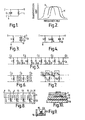
- Figure 1 shows part of a filter circuit comprising a capacitor C and an inductor L connected between input I and output O.
- the ciruit comprises a band pass type filter having a frequency response, of the type shown in solid outline in Figure 2.
- the cut-off frequencies are dependent on the value of inductance L and capacitance C, and thus if the capacitance changes with temperature the cut-off frequencies will change.
- a capacitor of the type shown in Figure 1 will have a frequency drift with temperature which is dependent on the dielectric material, D, used and the dimensions of the capacitor. This drift results from changes in the dielectric constant of the material as well as thermal expansions or contractions with temperature, all of which will change the capacitance.
- the dotted line response curves shown in Figure 2 represent a typical frequency response at different temperatures above Y and below X ambient temperature and the solid line shows the frequency response at ambient temperature.
- FIGs 3 and 4 show temperature compensating capacitor devices according to the invention which have a reduced temperature drift.
- the devices are connected in filter circuit sections with inductor L.
- Each capacitor device comprises a first capacitor C D of 'one dielectric material D, and a second capacitor C of another dielectric material A.
- the capacitors C and C D are connected in series and in Figure 4 the capacitors C A and C D are connected in parallel.
- the series arrangement or Figure 3 is useful for high frequency filters as it enables physically larger capacitors, which are easier to manufacture, to be used.
- the capacitors C A and C D are chosen such that the overall capacitance of the circuit remains substantially constant with temperature changes. This is achieved by suitable choice of the dielectric materials and dimensions of the capacitors.
- the dielectric material of the first capacitor C D is Duroid TM 5880 or 6010.5 and the dielectric material of the second capacitor C A is alumina.
- DuroidTM 5880 is a PTFE/teflon based material and a dielectric layer of this material will have fibers running in the X and Y longitudinal directions but none in the transverse Z, or thickness, direction. Thus when the temperature increases, expansion in the Z direction will be to a greater degree than expansions in the X and Y, or area, directions. Referring to equation (5) above, it can be seen that if d increases at a faster rate than A the capacitance will decrease. In an alumina capacitor which has a uniform dielectric, the opposite effect will occur, and the capacitance increases with increasing temperature.
- a capacitance which produces a much stant response with temperature can be produced by a combination of alumina and Duroid capacitors.
- the total capacitance C is given by
- the desired ratio for the parallel arrangement can be achieved by having a thickness between the capacitor plates of approximately 0.005 inches for the D uroid TM capacitor and of approximately 0.01 inches for the alumina capacitor, since the relative dielectric constant of alumina and Duroid are 10 and 2.2, respectively.
- capacitors C A and C D are coupled in parallel to provide a narrow band, filter.
- Figure 6 shows a modification of the Figure 5 arrangement, where C and C O are connected in series and adjacent, sections are coupled together by capacitors C S .
- the coupling capacitors in this arrangement are usually very small, which can make their physical realization difficult, particularly when laser or diamond saw cutting techniques are used in their manufacture as the tolerances required are very severe.
- Figure 7 shows a further modification where this problem is reduced.
- the coupling capacitor C S is connected between the midpoints of capacitors C A and C D in adjacent sections. This allows the capacitors to be larger while still providing the desired reduction in temperature drift, and thus the manufacturing tolerances are reduced to values as much as ten times less critical than in the Figure 5 and 6 embodiments.
- a method of constructing ladder network filters of the type shown in Figures 5, 6 and 7 will now be described with reference to Figures 8 and 9.
- the circuit sections are mounted in and connected to a housing 10 of conductive material such as brass or aluminum.
- Input and outlet terminations (not shown) for connection to suitable coaxial feeds will be provided at opposite ends of the housing and connected to opposite ends of the ladder network.
- the capacitors C are formed by etching one face of a layer 11 of the first dielectic material which is coated on both sides with conductive material 12. Capacitors C are defined between areas 13 of conductive material left by the etching and the underlying areas of the unetched face of the conductive coating.
- the dielectric material layer 11 is D uroid TM , which may be coated on both sides with copper, for example.
- the layer 11 is attached to the base of housing 10, for example by soldering.
- the capacitors C A 15 may be formed by cutting out capacitors of suitable sizes with a laser or diamond saw from sheets of the material A having a conductive coating on both sides.
- the material A is alumina and the conductive coating may, for example, be copper.
- Capacitors C A 15 are soldered to respective conductive areas 13 of the upper face of layer 11, as shown in Figure 8.
- the inductors L are then attached, for example by soldering, between capacitors C A 15 and the side walls of housing 10.
- Adjacent circuit sections in the ladder may be coupled together by attaching suitable coupling capacitors (not shown), such as leaf springs, between them.
- Such filter circuits may be designed and manufactured to produce any desired frequency response, but they are particularly useful as filter circuits for the 70 MHz to 18 GHz frequency range.
- the specific materials used in the preferred embodiment have been described above, it will be understood that alternative materials having the desired characteristics may be used for the dielectric materials, conductive coatings and conductive housing.
- the dielectric materials chosen must be such that in combination they produce the desired, substantially, constant capacitance and consequent reduction in temperature drift.
- Figures 10 to 12 illustrate a modified method of constructing ladder network filters according to the invention.
- the capacitors C D are formed by etching the upper face of a layer 11 of the material D, preferably Duroid, which is coated with conductive material, 12 suitably copper, on its opposite faces.
- Layer 11 is attached to the base of a housing 10, as in Figure 8, with its etched face 14 uppermost.
- Capacitors C A are formed by etching both upper and lower faces of a layer 17 of dielectric material A coated with conductive material. As in the previous embodiments material A is preferably alumina and the coating is preferably copper. Capacitors C A are defined between opposed areas of conductive material on opposite faces of layer 17. Layer 17 is then attached to layer 11, for example by soldering, so that capacitors C contact capacitors C A .
- An advantage of this construction in addition to the reduced temperature drift, is that it enables alumina -capacitors to be manufactured by photoetching a conductively coated sheet of alumina and to be attached in a housing without any necessity for a carrier to protect the brittle alumina from thermal expansion and contraction stresses.
- alumina capacitors were mounted in housings of materials having high coefficients of thermal expansion, carriers of Kovar (Registered Trade Mark) were used between the capacitors and the housing. The alumina capacitors could not be soldered directly to the housing as thermal expansion of the housing material could result in break up of the brittle alumina.
- duroid itself acts to cushion the alumina from thermal expansion and contraction stresses, since duroid is a non-rigid somewhat flexible material which can absorb such expansions and contractions.
- Figures 11 and 12 illustrate a coupling connection between adjacent sections of a ladder circuit constructed from two etched layers.
- the upper face of layer 15 is etched so as to form conductive bridge areas 16 between adjacent capacitors C A .
- FIG. 13 A ladder circuit which can be constructed in this way is shown in Figure 13.
- Figures 13A and 13B show the etching of coated layers 11 and 15 to form the circuit of Figure 13.
- Figure 13A shows the etching of the top face 27 of layer 11, which is preferably a Duroid material layer, to form conductive areas 18.
- Figure 13B shows the lower face of layer 17 is identical to the upper face of layer 11.
- Figure 13C shows the etching of the upper face 21 of layer 15 to form conductive areas 22.
- the various capacitors of the circuit shown in Figure 13 are defined by the overlap between the various etched conductive areas.
- the capacitors C A labeled 1, 2 and 3 in Figure 13 are defined between the conductive areas labeled 1, 2 and 3 on the opposing faces of layer 17, as shown in Figures 13A and 13B.
- the linking capacitors between adjacent sections of the ladder network are formed by conductive bridge area 4 on the - upper face 21 of layer 17 (see Figure 13C), in the manner described above in connection with Figures 11 and 12.
- Inductors L are soldered between the capacitors C A numbered 3 in the drawings, and the side wall of the housing.
- Figure 13A shows an input pin 23 whicn is attached to the first conductive area 18 on face 11.
- the ideal frequency response of a band pass filter is rectangular.
- the sides of the characteristic response will be sloping and the center portion will not be flat, due to the delay time of the filter being slightly different at different frequencies, combined with the fact that the elements in the filter are not entirely lossless.
- One way of improving the frequency response by steepening the slide slopes and flattening the top of the curve is to add more sections to the ladder network and widening the filter bandwidth. However this results in some signal losses.
- Another way of making the frequency response more "square” is to inductively cross- couple the end sections of a capacitively coupled ladder network to produce a so-called quasi-elliptic function filter.
- Figure 14 shows a circuit comprising a ladder network including filter sections having different material capacitors C A and C D as described above, and an inductive cross-coupling Ll, L2, L3, L4, L5 between the end sections of the ladder network.
- a method of constructing the circuit of Figure 14 can be seen in Figure 15 which shows the series capacitors are realized using small coupling wires soldered to the shunt alumina capacitors at one end.
- capacitors C D are formed by etching one face of a layer 11 of dielectric material D, which is preferably Duroid, to form conductive areas 24. Layer 11 is additionally etched to form a copper coupling line 25.
- Alumina capacitors C A formed either separately as described in connection with Figures 8 and 9 or by etching a coated layer of alumina as described in connection with Figures 10 to 12 above, are attached to the Duroid layer.
- the capacitors C of the end sections of the ladder are attached by inductors Ll and L2 to intermediate points X on the coupling line 25.
- Effective inductor L3 is defined between points X on the coupling line
- effective inductors L4 and L5 are defined between the side walls of the housing and points X.
- Inductances L3, L4 and L5 formed by coupling line 25 are much smaller than helically wound inductances Ll and L2.
- the inductively cross-coupled circuit described above enables a ladder network with a lower number of sections to produce a specified frequency response. This results in a small size and less expensive filter, and a reduced loss of signal for the same frequency response.
- the frequency response will approximate more closely to the desired square function for a band pass filter, and an asymmetric response may be produced if desired by the provision of suitable numbers of filter sections.
- the cross-coupling can also result in substantial amplitude and phase equalization. This is particularly useful for many microwave filters, since such filters have problems of phase shift as a result of different frequencies passing through the filter with different delay times. If the coefficient of thermal of expansion of area of the dielectric is A , and that of its depth is ⁇ d, then form equation (5) the capacitance varies as: . If then the capacitance will remain constant with temperature, dielectric has such properties, but, in accordance with the invention, a suitably chosen composite of two or more dielectrics can approximate to the above.
Landscapes
- Engineering & Computer Science (AREA)
- Power Engineering (AREA)
- Manufacturing & Machinery (AREA)
- Microelectronics & Electronic Packaging (AREA)
- Fixed Capacitors And Capacitor Manufacturing Machines (AREA)
- Oscillators With Electromechanical Resonators (AREA)
- Filters And Equalizers (AREA)
- Amplifiers (AREA)
Priority Applications (1)
| Application Number | Priority Date | Filing Date | Title |
|---|---|---|---|
| AT84302002T ATE54038T1 (de) | 1983-09-27 | 1984-03-26 | Temperaturkompensierter kondensator. |
Applications Claiming Priority (2)
| Application Number | Priority Date | Filing Date | Title |
|---|---|---|---|
| GB8325786 | 1983-09-27 | ||
| GB8325786 | 1983-09-27 |
Publications (3)
| Publication Number | Publication Date |
|---|---|
| EP0140462A2 true EP0140462A2 (fr) | 1985-05-08 |
| EP0140462A3 EP0140462A3 (en) | 1986-12-17 |
| EP0140462B1 EP0140462B1 (fr) | 1990-06-20 |
Family
ID=10549339
Family Applications (1)
| Application Number | Title | Priority Date | Filing Date |
|---|---|---|---|
| EP84302002A Expired - Lifetime EP0140462B1 (fr) | 1983-09-27 | 1984-03-26 | Condensateur compensé en fonction de la température |
Country Status (4)
| Country | Link |
|---|---|
| US (1) | US4581795A (fr) |
| EP (1) | EP0140462B1 (fr) |
| AT (1) | ATE54038T1 (fr) |
| DE (1) | DE3482564D1 (fr) |
Cited By (1)
| Publication number | Priority date | Publication date | Assignee | Title |
|---|---|---|---|---|
| US4939486A (en) * | 1988-01-04 | 1990-07-03 | Asea Brown Boveri Ab | Filter equipment for power lines |
Families Citing this family (9)
| Publication number | Priority date | Publication date | Assignee | Title |
|---|---|---|---|---|
| US4714905A (en) * | 1986-10-08 | 1987-12-22 | K & L Microwave | SMC filter and method of manufacture thereof |
| US4910516A (en) * | 1987-03-25 | 1990-03-20 | Texas Instruments Incorporated | Integrated dual-slope analog to digital converter with R/C variance compensation |
| US4849757A (en) * | 1987-03-25 | 1989-07-18 | Texas Instruments Incorporated | Integrated dual-slope analog to digital converter with r/c variance compensation |
| US4807477A (en) * | 1988-02-01 | 1989-02-28 | Motorola, Inc. | Capacitive temperature compensation for a pressure sensor |
| US4939779A (en) * | 1989-05-19 | 1990-07-03 | Hitchcock Bernard K | Temperature compensated trap filter |
| US5021795A (en) * | 1989-06-23 | 1991-06-04 | Motorola, Inc. | Passive temperature compensation scheme for microstrip antennas |
| CN103782665B (zh) * | 2011-08-15 | 2017-04-26 | 艾思玛太阳能技术股份公司 | 在电路板的支持物中包括电容器的电子设备及其生产方法 |
| CN103066859A (zh) * | 2011-10-19 | 2013-04-24 | 台达电子企业管理(上海)有限公司 | 一种大功率高压变频器功率单元 |
| US11087731B2 (en) | 2014-07-23 | 2021-08-10 | Donald L Baker | Humbucking pair building block circuit for vibrational sensors |
Family Cites Families (11)
| Publication number | Priority date | Publication date | Assignee | Title |
|---|---|---|---|---|
| GB598817A (en) * | 1945-09-12 | 1948-02-26 | British Insulated Callenders | Improvements in electric capacitors |
| FR784930A (fr) * | 1934-02-01 | 1935-07-29 | Porzellanfabrik Kahla | Disposition pour circuits de condensateurs et circuits oscillants indépendants de la température |
| CH245815A (de) * | 1943-06-30 | 1946-11-30 | Fides Gmbh | Kondensator mit geringen dielektrischen Verlusten und kleinem Temperaturgang der Kapazität. |
| DE914287C (de) * | 1944-11-15 | 1954-06-28 | Telefunken Gmbh | Elektrisches Filter, welches einen glockenfoermigen Ausgangsimpuls liefert |
| US3012176A (en) * | 1955-03-29 | 1961-12-05 | Hunt Capacitors Ltd A | Electrical capacitors |
| US3273033A (en) * | 1963-08-29 | 1966-09-13 | Litton Systems Inc | Multidielectric thin film capacitors |
| US3289059A (en) * | 1965-05-05 | 1966-11-29 | Sprague Electric Co | Dry film capacitor |
| US3408590A (en) * | 1966-10-31 | 1968-10-29 | Bell Telephone Labor Inc | Active hybrid filter using frequency emphasizing and attenuating networks |
| JPS4870855A (fr) * | 1971-12-29 | 1973-09-26 | ||
| US3720887A (en) * | 1972-02-22 | 1973-03-13 | Microsystems Int Ltd | Frequency determining network |
| US3960043A (en) * | 1974-06-24 | 1976-06-01 | Warwick Electronics Inc. | Filter circuit |
-
1984
- 1984-03-26 DE DE8484302002T patent/DE3482564D1/de not_active Expired - Lifetime
- 1984-03-26 EP EP84302002A patent/EP0140462B1/fr not_active Expired - Lifetime
- 1984-03-26 AT AT84302002T patent/ATE54038T1/de not_active IP Right Cessation
- 1984-04-30 US US06/605,383 patent/US4581795A/en not_active Expired - Fee Related
Cited By (1)
| Publication number | Priority date | Publication date | Assignee | Title |
|---|---|---|---|---|
| US4939486A (en) * | 1988-01-04 | 1990-07-03 | Asea Brown Boveri Ab | Filter equipment for power lines |
Also Published As
| Publication number | Publication date |
|---|---|
| EP0140462A3 (en) | 1986-12-17 |
| EP0140462B1 (fr) | 1990-06-20 |
| ATE54038T1 (de) | 1990-07-15 |
| US4581795A (en) | 1986-04-15 |
| DE3482564D1 (de) | 1990-07-26 |
Similar Documents
| Publication | Publication Date | Title |
|---|---|---|
| US4423396A (en) | Bandpass filter for UHF band | |
| US3879690A (en) | Distributed transmission line filter | |
| US4992759A (en) | Filter having elements with distributed constants which associate two types of coupling | |
| EP1536558B1 (fr) | Symétriseur | |
| US5760663A (en) | Elliptic baw resonator filter and method of making the same | |
| US5621366A (en) | High-Q multi-layer ceramic RF transmission line resonator | |
| US20040251992A1 (en) | Multilayer waveguide filter employing via metals | |
| JP2558419B2 (ja) | 広帯域マイクロ波フィルタネットワーク | |
| US4731596A (en) | Band-pass filter for hyperfrequencies | |
| US5448209A (en) | Laminated dielectric filter | |
| EP0140462B1 (fr) | Condensateur compensé en fonction de la température | |
| WO2022152178A1 (fr) | Filtre, multiplexeur et dispositif électronique | |
| US8120446B2 (en) | Electronic component | |
| US4110715A (en) | Broadband high pass microwave filter | |
| US5032810A (en) | LC filter | |
| US11711063B2 (en) | Multilayer filter device | |
| US4636913A (en) | Temperature compensated capacitor | |
| CN111697293A (zh) | 一种小型化低损耗的ltcc带通滤波器 | |
| RU2829490C1 (ru) | Высокоизбирательный микрополосковый полосно-пропускающий фильтр | |
| JP2737063B2 (ja) | ストリップラインフィルタ | |
| JP2737062B2 (ja) | ストリップラインフィルタ | |
| US6281763B1 (en) | Dielectric resonator, dielectric filter, dielectric duplexer, and method for manufacturing dielectric resonator | |
| JP2006067221A (ja) | 積層型誘電体フィルタ | |
| CN101420214B (zh) | 指间相连式的层叠带通滤波器 | |
| CN116886072A (zh) | 梯型结构滤波器、形成方法、多工器及电子设备 |
Legal Events
| Date | Code | Title | Description |
|---|---|---|---|
| PUAI | Public reference made under article 153(3) epc to a published international application that has entered the european phase |
Free format text: ORIGINAL CODE: 0009012 |
|
| AK | Designated contracting states |
Designated state(s): AT BE CH DE FR GB IT LI LU NL SE |
|
| PUAL | Search report despatched |
Free format text: ORIGINAL CODE: 0009013 |
|
| AK | Designated contracting states |
Kind code of ref document: A3 Designated state(s): AT BE CH DE FR GB IT LI LU NL SE |
|
| 17P | Request for examination filed |
Effective date: 19870414 |
|
| 17Q | First examination report despatched |
Effective date: 19890120 |
|
| GRAA | (expected) grant |
Free format text: ORIGINAL CODE: 0009210 |
|
| AK | Designated contracting states |
Kind code of ref document: B1 Designated state(s): AT BE CH DE FR GB IT LI LU NL SE |
|
| PG25 | Lapsed in a contracting state [announced via postgrant information from national office to epo] |
Ref country code: SE Effective date: 19900620 Ref country code: NL Effective date: 19900620 Ref country code: LI Effective date: 19900620 Ref country code: IT Free format text: LAPSE BECAUSE OF FAILURE TO SUBMIT A TRANSLATION OF THE DESCRIPTION OR TO PAY THE FEE WITHIN THE PRESCRIBED TIME-LIMIT;WARNING: LAPSES OF ITALIAN PATENTS WITH EFFECTIVE DATE BEFORE 2007 MAY HAVE OCCURRED AT ANY TIME BEFORE 2007. THE CORRECT EFFECTIVE DATE MAY BE DIFFERENT FROM THE ONE RECORDED. Effective date: 19900620 Ref country code: FR Effective date: 19900620 Ref country code: CH Effective date: 19900620 Ref country code: BE Effective date: 19900620 Ref country code: AT Effective date: 19900620 |
|
| REF | Corresponds to: |
Ref document number: 54038 Country of ref document: AT Date of ref document: 19900715 Kind code of ref document: T |
|
| REF | Corresponds to: |
Ref document number: 3482564 Country of ref document: DE Date of ref document: 19900726 |
|
| REG | Reference to a national code |
Ref country code: CH Ref legal event code: PL |
|
| EN | Fr: translation not filed | ||
| NLV1 | Nl: lapsed or annulled due to failure to fulfill the requirements of art. 29p and 29m of the patents act | ||
| PG25 | Lapsed in a contracting state [announced via postgrant information from national office to epo] |
Ref country code: GB Effective date: 19910326 |
|
| PG25 | Lapsed in a contracting state [announced via postgrant information from national office to epo] |
Ref country code: LU Free format text: LAPSE BECAUSE OF NON-PAYMENT OF DUE FEES Effective date: 19910331 |
|
| PLBE | No opposition filed within time limit |
Free format text: ORIGINAL CODE: 0009261 |
|
| STAA | Information on the status of an ep patent application or granted ep patent |
Free format text: STATUS: NO OPPOSITION FILED WITHIN TIME LIMIT |
|
| 26N | No opposition filed | ||
| GBPC | Gb: european patent ceased through non-payment of renewal fee | ||
| PG25 | Lapsed in a contracting state [announced via postgrant information from national office to epo] |
Ref country code: DE Effective date: 19920101 |