EP0140677B1 - Amplificateur différentiel utilisant une source de courant constant - Google Patents
Amplificateur différentiel utilisant une source de courant constant Download PDFInfo
- Publication number
- EP0140677B1 EP0140677B1 EP84307366A EP84307366A EP0140677B1 EP 0140677 B1 EP0140677 B1 EP 0140677B1 EP 84307366 A EP84307366 A EP 84307366A EP 84307366 A EP84307366 A EP 84307366A EP 0140677 B1 EP0140677 B1 EP 0140677B1
- Authority
- EP
- European Patent Office
- Prior art keywords
- transistor
- voltage power
- power terminal
- resistor
- mos transistor
- Prior art date
- Legal status (The legal status is an assumption and is not a legal conclusion. Google has not performed a legal analysis and makes no representation as to the accuracy of the status listed.)
- Expired
Links
Images



Classifications
-
- H—ELECTRICITY
- H03—ELECTRONIC CIRCUITRY
- H03F—AMPLIFIERS
- H03F1/00—Details of amplifiers with only discharge tubes, only semiconductor devices or only unspecified devices as amplifying elements
- H03F1/30—Modifications of amplifiers to reduce influence of variations of temperature or supply voltage or other physical parameters
-
- H—ELECTRICITY
- H03—ELECTRONIC CIRCUITRY
- H03F—AMPLIFIERS
- H03F3/00—Amplifiers with only discharge tubes or only semiconductor devices as amplifying elements
- H03F3/45—Differential amplifiers
- H03F3/45071—Differential amplifiers with semiconductor devices only
- H03F3/45076—Differential amplifiers with semiconductor devices only characterised by the way of implementation of the active amplifying circuit in the differential amplifier
- H03F3/45179—Differential amplifiers with semiconductor devices only characterised by the way of implementation of the active amplifying circuit in the differential amplifier using MOSFET transistors as the active amplifying circuit
- H03F3/45183—Long tailed pairs
-
- G—PHYSICS
- G05—CONTROLLING; REGULATING
- G05F—SYSTEMS FOR REGULATING ELECTRIC OR MAGNETIC VARIABLES
- G05F3/00—Non-retroactive systems for regulating electric variables by using an uncontrolled element, or an uncontrolled combination of elements, such element or such combination having self-regulating properties
- G05F3/02—Regulating voltage or current
- G05F3/08—Regulating voltage or current wherein the variable is DC
- G05F3/10—Regulating voltage or current wherein the variable is DC using uncontrolled devices with non-linear characteristics
- G05F3/16—Regulating voltage or current wherein the variable is DC using uncontrolled devices with non-linear characteristics being semiconductor devices
- G05F3/20—Regulating voltage or current wherein the variable is DC using uncontrolled devices with non-linear characteristics being semiconductor devices using diode- transistor combinations
- G05F3/22—Regulating voltage or current wherein the variable is DC using uncontrolled devices with non-linear characteristics being semiconductor devices using diode- transistor combinations wherein the transistors are of the bipolar type only
- G05F3/222—Regulating voltage or current wherein the variable is DC using uncontrolled devices with non-linear characteristics being semiconductor devices using diode- transistor combinations wherein the transistors are of the bipolar type only with compensation for device parameters, e.g. Early effect, gain, manufacturing process, or external variations, e.g. temperature, loading, supply voltage
- G05F3/225—Regulating voltage or current wherein the variable is DC using uncontrolled devices with non-linear characteristics being semiconductor devices using diode- transistor combinations wherein the transistors are of the bipolar type only with compensation for device parameters, e.g. Early effect, gain, manufacturing process, or external variations, e.g. temperature, loading, supply voltage producing a current or voltage as a predetermined function of the temperature
-
- G—PHYSICS
- G05—CONTROLLING; REGULATING
- G05F—SYSTEMS FOR REGULATING ELECTRIC OR MAGNETIC VARIABLES
- G05F3/00—Non-retroactive systems for regulating electric variables by using an uncontrolled element, or an uncontrolled combination of elements, such element or such combination having self-regulating properties
- G05F3/02—Regulating voltage or current
- G05F3/08—Regulating voltage or current wherein the variable is DC
- G05F3/10—Regulating voltage or current wherein the variable is DC using uncontrolled devices with non-linear characteristics
- G05F3/16—Regulating voltage or current wherein the variable is DC using uncontrolled devices with non-linear characteristics being semiconductor devices
- G05F3/20—Regulating voltage or current wherein the variable is DC using uncontrolled devices with non-linear characteristics being semiconductor devices using diode- transistor combinations
- G05F3/24—Regulating voltage or current wherein the variable is DC using uncontrolled devices with non-linear characteristics being semiconductor devices using diode- transistor combinations wherein the transistors are of the field-effect type only
- G05F3/242—Regulating voltage or current wherein the variable is DC using uncontrolled devices with non-linear characteristics being semiconductor devices using diode- transistor combinations wherein the transistors are of the field-effect type only with compensation for device parameters, e.g. channel width modulation, threshold voltage, processing, or external variations, e.g. temperature, loading, supply voltage
- G05F3/245—Regulating voltage or current wherein the variable is DC using uncontrolled devices with non-linear characteristics being semiconductor devices using diode- transistor combinations wherein the transistors are of the field-effect type only with compensation for device parameters, e.g. channel width modulation, threshold voltage, processing, or external variations, e.g. temperature, loading, supply voltage producing a voltage or current as a predetermined function of the temperature
-
- H—ELECTRICITY
- H03—ELECTRONIC CIRCUITRY
- H03F—AMPLIFIERS
- H03F1/00—Details of amplifiers with only discharge tubes, only semiconductor devices or only unspecified devices as amplifying elements
- H03F1/30—Modifications of amplifiers to reduce influence of variations of temperature or supply voltage or other physical parameters
- H03F1/301—Modifications of amplifiers to reduce influence of variations of temperature or supply voltage or other physical parameters in MOSFET amplifiers
-
- H—ELECTRICITY
- H03—ELECTRONIC CIRCUITRY
- H03F—AMPLIFIERS
- H03F3/00—Amplifiers with only discharge tubes or only semiconductor devices as amplifying elements
- H03F3/45—Differential amplifiers
- H03F3/45071—Differential amplifiers with semiconductor devices only
- H03F3/45076—Differential amplifiers with semiconductor devices only characterised by the way of implementation of the active amplifying circuit in the differential amplifier
- H03F3/4508—Differential amplifiers with semiconductor devices only characterised by the way of implementation of the active amplifying circuit in the differential amplifier using bipolar transistors as the active amplifying circuit
- H03F3/45085—Long tailed pairs
-
- H—ELECTRICITY
- H03—ELECTRONIC CIRCUITRY
- H03F—AMPLIFIERS
- H03F2203/00—Indexing scheme relating to amplifiers with only discharge tubes or only semiconductor devices as amplifying elements covered by H03F3/00
- H03F2203/45—Indexing scheme relating to differential amplifiers
- H03F2203/45456—Indexing scheme relating to differential amplifiers the CSC comprising bias stabilisation means, e.g. DC-level stability, positive or negative temperature coefficient dependent control
-
- H—ELECTRICITY
- H03—ELECTRONIC CIRCUITRY
- H03F—AMPLIFIERS
- H03F2203/00—Indexing scheme relating to amplifiers with only discharge tubes or only semiconductor devices as amplifying elements covered by H03F3/00
- H03F2203/45—Indexing scheme relating to differential amplifiers
- H03F2203/45702—Indexing scheme relating to differential amplifiers the LC comprising two resistors
Definitions
- the present invention relates to a differential amplifier which uses a constant-current source circuit.
- Known constant-current source circuits can generate a current relatively stable against variations of power supply voltage, but not that stable against variations in the ambient temperature.
- a constant-current source circuit is typically used in an emitter-coupled-logic (ECL) circuit. Even a slight change in the current of the constant-current source circuit will result in a change in the logic level voltages of the output signal of the ECL circuit, especially when many ECL circuits are coupled in cascade, thereby reducing the voltage margin of the ECL circuit.
- ECL emitter-coupled-logic
- the temperature characteristic of the output current is compensated for by using the temperature characteristic of the forward-biased voltage of a diode or of the base-emitter voltage of a bipolar transistor.
- the output current is stabilized by using a negative feedback circuit.
- JP-A-58-35614 discloses an integrated reference voltage and current supply circuit, which operates reliably with a low power source voltage by synthesizing currents from constant voltage circuits having both negative and positive temperature coefficients, to form the reference voltage or current.
- a differential amplifier comprising a pair of differential transistors whose sources or emitters are commonly connected, and a constant-current source circuit connected to the common connection point, said circuit including:
- the present invention adopts the idea of synthesizing the outputs of a plurality of constant-current source circuit units, having different temperature coefficients, in a constant-current source circuit.
- An embodiment of the present invention can completely compensate for the temperature characteristic of the output current of a constant-current source circuit or to adjust it to a desired characteristic.
- An embodiment of the present invention can completely compensate for the temperature characteristic of a circuit using a constant-current source circuit or to adjust the temperature characteristic of the circuit to a desired one.
- a conventional amplifier includes transistors Q a and Q b , whose sources are mutually connected, a transistor Q c for a constant-current source, and load resistors R 1 and R 2 .
- the drain of the transistor Q c is connected to the commonly connected sources of the transistors Q a and Q b , and the source and the gate of the transistor Q c are connected to a power source V ss and a reference voltage V REF , respectively.
- the high level voltage V OH of each of output signals V 01 and V 02 is approximately equal to a power supply voltage V cc .
- the low level voltage V OL of each output signal V 01 or V 02 depends on the impedances of the transistor Q a or Q b and the transistor Q c . For example, when an input signal V IN1 is low and an input signal V IN2 is high, the transistor Q b is turned on and the output signal V 02 becomes low.
- the impedance of the turned-on MOS transistors Q b and Q c increases in accordance with a temperature rise, because the carrier mobility in the channel region becomes small when the ambient temperature is high. Therefore, as illustrated in Fig. 2, the low level voltage V OL of the output signal of the circuit of Fig. 1 increases in accordance with the rise of the ambient temperature T.
- an improved differential amplifier using a constant-current source circuit to overcome the above-mentioned problems of the conventional circuit.
- FIG. 3 illustrates the principle of a constant-current source circuit in an embodiment of the present invention.
- the circuit of Fig. 3 comprises a differential circuit A 1 such as a current switch or a differential amplifier, a parallel circuit of MOS transistors Q, and Q 2 inserted between the common emitter or the common source of the differential circuit A 1 and a power source V ss , a constant-current source circuit unit CS, which is connected to the gate of the transistor Q, and which has a positive temperature coefficient, and a constant-current source circuit unit CS 2 which is connected to the gate of the transistor Q 2 and which has a negative temperature coefficient.
- the constant-current source circuit units CS 1 and CS 2 may be combined with the transistors Q, and Q 2 , respectively, to constitute a constant-current source circuit or may supply control voltages to the gates of the transistors Q, and Q 2 to control the output current of these transistors, respectively.
- the drain current IS 1 of the transistor Q 1 is controlled by the constant-current source circuit unit CS 1 , the drain current IS 1 has, as shown in Fig. 4, a positive temperature coefficient.
- the drain current IS 2 has a negative temperature coefficient, because it is controlled by the constant-current source circuit unit CS 2 . Therefore, it is possible to obtain an output current IS having a zero temperature coefficient, as shown in Fig. 4, or any desired temperature coefficient by synthesizing (combining) these currents IS 1 and IS 2 using a current synthesizing circuit constituted of the transistors Q, and Q 2 .
- FIG. 5 illustrates a detailed structure of a differential amplifier which uses a constant-current source circuit in an embodiment of the present invention.
- the circuit of Fig. 5 includes a differential circuit A 1 having differential transistors Q 3 and Q 4 whose sources are commonly connected to each other and load resistors R, and R 2 ; N-channel MOS transistors Q 5 and Q 6 , and resistors R 3 and R 4 constituting a constant-current source circuit unit CS 2 which is connected to the common source of the transistors Q 3 and Q 4 and which has a negative temperature coefficient; N-channel MOS transistor Q 8 , P-channel MOS transistors Qg and Q 10 , and resistors R 5 and R 6 composing a constant-current source circuit unit CS, having a positive temperature coefficient; and an N-channel MOS transistor Q 7 composing a current synthesizing circuit.
- the transistor Q 5 is used as a part of the current synthesizing circuit and as a part of the constant-current source circuit and CS 2 .
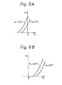
- the drain current I D of each of the P-channel MOS transistors Qg and Q 10 of the constant-current source circuit unit CS 1 increases (at the same gate voltage V G ) in accordance with a temperature rise.
- the higher the temperature the smaller the probability of activation of holes in the channel area and thus the greater the absolute value of the threshold voltage. Therefore, the higher the temperature, the more current flows through the resistor R 5 and the more current flows through the transistor Q 8 . Since the transistor Q 8 and the transistor Q 7 constitute a current mirror circuit, the current IS 1 flowing through the transistor Q 7 increases in accordance with the temperature rise. Therefore, the constant-current source circuit unit CS 1 operates so as to lower the potential of output voltages V 01 and V 02 of the differential circuit in accordance with a temperature rise.
- the threshold value of the gate voltage of the N-channel MOS transistor Q 6 becomes low in accordance with a temperature rise. This is because, in an N-channel MOS transistor, the higher the temperature, the greater the probability of activation of electrons in a channel area. Therefore, the current flowing through the resistor R 4 , i.e., the output current IS 2 of the constant-current source circuit unit CS 2 , decreases in accordance with a temperature rise. That is, the constant-current source circuit unit CS 2 operates so as to increase the output voltages V 01 and V o2 of the differential circuit in accordance with a temperature rise.
- Figure 7 illustrates a differential amplifier as another embodiment of the present invention.
- the circuit of Fig. 7 is the same as that of Fig. 5, except that the constant-current source circuit unit CS 2 of Fig. 5 is omitted.
- the output current IS 1 of the constant-current source circuit unit CS 1 increases in accordance with a temperature rise, thus lowering the output voltage V 01 or V o2 , it is possible to stabilize the output voltage, for example, V 02 of the differential amplifier of Fig. 7.
- V 02 the differential amplifier of Fig. 7.
- the gradient of the output voltage V 02 can be adjusted to any value by adjusting the resistance of the resistors R 2 and R 5 .
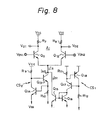
- Figure 8 illustrates a differential amplifier using a constant-current source circuit in another embodiment of the present invention.
- the circuit of Fig. 8 corresponds to the circuit of Fig. 5, except the P-channel MOS transistors are replaced by PNP-type bipolar transistors and the N-channel MOS transistors are replaced by NPN-type bipolar transistors. Since the threshold value characteristic of a PNP-type bipolar transistor, i.e., the base voltage to collector current characteristic thereof, is similar to the threshold value characteristic of a P-channel MOS transistor and since the threshold value characteristic of an NPN-type bipolar transistor is similar to the threshold value characteristic of an N-channel MOS transistor, it is clearly possible to obtain a characteristic similarto that of the circuit of Fig. 5 in the circuit of Fig. 8.
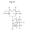
- Figure 9 illustrates a differential amplifier using a constant-current source in a further embodiment of the present invention.
- the circuit of Fig. 9 is the same as that of Fig. 8, except that the constant-current source circuit unit CS 2 is omitted.
- the circuit of Fig. 9 corresponds to the circuit of Fig. 7. Thus, a detailed explanation thereof is omitted.
- generating a current output by synthesizing the output currents of a plurality of constant current source circuit units having different temperature coefficients enables realization of an output current having any desired temperature coefficient in accordance with the characteristic, the condition of usage, and the like of an ECL circuit and so on and enables complete temperature compensation of each parameter of an integrated circuit device and so on.
- a differential amplifier according to the present invention wherein a single constant-current source circuit unit is used, it is possible to effect temperature compensation appropriately by using a simple circuit structure. Since the temperature compensation is effected by using the temperature characteristic of the gate threshold voltage, which is inherent in the nature a device, such as a MOS transistor or a bipolar transistor, the spread of the temperature characteristic of circuits can be made very small.
- a differential amplifier which uses a constant-current source circuit in accordance with the present invention, it is possible to ensure a stable temperature characteristic of, for example, the potentials of its logic output signals.
Landscapes
- Engineering & Computer Science (AREA)
- Microelectronics & Electronic Packaging (AREA)
- Physics & Mathematics (AREA)
- Power Engineering (AREA)
- Radar, Positioning & Navigation (AREA)
- General Physics & Mathematics (AREA)
- Electromagnetism (AREA)
- Automation & Control Theory (AREA)
- Nonlinear Science (AREA)
- Amplifiers (AREA)
- Control Of Electrical Variables (AREA)
- Continuous-Control Power Sources That Use Transistors (AREA)
- Logic Circuits (AREA)
Claims (5)
dans lequel un courant de sortie de l'une des unités de source à courant constant est commandé par la caractéristique de tension de seuil d'un transistor MOS à canal P ou par un transistor de type PNP, et un courant de sortie de l'autre unité de source à courant constant est commandé par la caractéristique de tension de seuil d'un transistor MOS à canal N ou par un transistor de type NPN.
Applications Claiming Priority (2)
| Application Number | Priority Date | Filing Date | Title |
|---|---|---|---|
| JP200045/83 | 1983-10-27 | ||
| JP58200045A JP2525346B2 (ja) | 1983-10-27 | 1983-10-27 | 定電流源回路を有する差動増幅回路 |
Publications (3)
| Publication Number | Publication Date |
|---|---|
| EP0140677A2 EP0140677A2 (fr) | 1985-05-08 |
| EP0140677A3 EP0140677A3 (en) | 1987-05-20 |
| EP0140677B1 true EP0140677B1 (fr) | 1991-01-09 |
Family
ID=16417904
Family Applications (1)
| Application Number | Title | Priority Date | Filing Date |
|---|---|---|---|
| EP84307366A Expired EP0140677B1 (fr) | 1983-10-27 | 1984-10-26 | Amplificateur différentiel utilisant une source de courant constant |
Country Status (6)
| Country | Link |
|---|---|
| US (1) | US4636742A (fr) |
| EP (1) | EP0140677B1 (fr) |
| JP (1) | JP2525346B2 (fr) |
| KR (1) | KR890004647B1 (fr) |
| CA (1) | CA1224543A (fr) |
| DE (1) | DE3483904D1 (fr) |
Families Citing this family (30)
| Publication number | Priority date | Publication date | Assignee | Title |
|---|---|---|---|---|
| US4677368A (en) * | 1986-10-06 | 1987-06-30 | Motorola, Inc. | Precision thermal current source |
| JPS63213493A (ja) * | 1987-03-02 | 1988-09-06 | Matsushita Electric Ind Co Ltd | 3相電流出力回路 |
| US4853646A (en) * | 1988-07-19 | 1989-08-01 | Fairchild Semiconductor Corporation | Temperature compensated bipolar circuits |
| US4970415A (en) * | 1989-07-18 | 1990-11-13 | Gazelle Microcircuits, Inc. | Circuit for generating reference voltages and reference currents |
| FR2653574B1 (fr) * | 1989-10-20 | 1992-01-10 | Sgs Thomson Microelectronics | Source de courant a faible coefficient de temperature. |
| DE69000803T2 (de) * | 1989-10-20 | 1993-06-09 | Sgs Thomson Microelectronics | Stromquelle mit niedrigem temperaturkoeffizient. |
| EP0450830B1 (fr) * | 1990-03-30 | 1996-10-23 | Texas Instruments Incorporated | Référence de tension avec coefficient de température à forte pente et méthode d'opération |
| JPH03296118A (ja) * | 1990-04-13 | 1991-12-26 | Oki Micro Design Miyazaki:Kk | 基準電圧発生回路 |
| US5068595A (en) * | 1990-09-20 | 1991-11-26 | Delco Electronics Corporation | Adjustable temperature dependent current generator |
| US5200654A (en) * | 1991-11-20 | 1993-04-06 | National Semiconductor Corporation | Trim correction circuit with temperature coefficient compensation |
| US5448770A (en) * | 1993-04-05 | 1995-09-05 | Motorola, Inc. | Temperature-coefficient controlled radio frequency signal detecting circuitry |
| US5410745A (en) * | 1993-05-20 | 1995-04-25 | Motorola, Inc. | Detector and video amplifier |
| JPH07225622A (ja) * | 1994-02-10 | 1995-08-22 | Fujitsu Ltd | 電界効果トランジスタを用いた定電流回路 |
| JP3479408B2 (ja) * | 1996-04-23 | 2003-12-15 | アルプス電気株式会社 | Agc電圧補正回路 |
| US5818294A (en) * | 1996-07-18 | 1998-10-06 | Advanced Micro Devices, Inc. | Temperature insensitive current source |
| US5856749A (en) * | 1996-11-01 | 1999-01-05 | Burr-Brown Corporation | Stable output bias current circuitry and method for low-impedance CMOS output stage |
| GB2332760A (en) * | 1997-12-24 | 1999-06-30 | Motorola Inc | Low voltage stabilised current source |
| US6265857B1 (en) | 1998-12-22 | 2001-07-24 | International Business Machines Corporation | Constant current source circuit with variable temperature compensation |
| US6087820A (en) * | 1999-03-09 | 2000-07-11 | Siemens Aktiengesellschaft | Current source |
| DE10066032B4 (de) | 2000-07-28 | 2010-01-28 | Infineon Technologies Ag | Schaltungsanordnung zur Steuerung der Verstärkung einer Verstärkerschaltung |
| JP4141111B2 (ja) * | 2001-03-29 | 2008-08-27 | 三洋電機株式会社 | 信号増幅装置 |
| DE10147101A1 (de) * | 2001-09-25 | 2003-04-24 | Infineon Technologies Ag | Temperaturstabilisierte Verstärkerschaltung |
| JP3874247B2 (ja) * | 2001-12-25 | 2007-01-31 | 株式会社ルネサステクノロジ | 半導体集積回路装置 |
| US6614305B1 (en) * | 2002-02-19 | 2003-09-02 | Texas Instruments Incorporated | Method and circuit for trimming offset and temperature drift for operational amplifiers and voltage references |
| US7236049B2 (en) * | 2003-03-20 | 2007-06-26 | Nxp B.V. | Circuit arrangement and transistor control method |
| JP4522299B2 (ja) * | 2005-03-29 | 2010-08-11 | 富士通セミコンダクター株式会社 | 定電流回路 |
| JP4755875B2 (ja) * | 2005-09-30 | 2011-08-24 | 三洋電機株式会社 | 温度補償回路 |
| US8072259B1 (en) * | 2008-04-30 | 2011-12-06 | Integrated Device Technology, Inc. | Voltage reference and supply voltage level detector circuits using proportional to absolute temperature cells |
| CN104765405B (zh) * | 2014-01-02 | 2017-09-05 | 意法半导体研发(深圳)有限公司 | 温度和工艺补偿的电流基准电路 |
| CN114812846B (zh) * | 2022-04-13 | 2023-03-24 | 湖南四灵电子科技有限公司 | 一种兼容正负温度系数传感器的温度采样电路 |
Family Cites Families (6)
| Publication number | Priority date | Publication date | Assignee | Title |
|---|---|---|---|---|
| US3431508A (en) * | 1966-03-16 | 1969-03-04 | Honeywell Inc | Ph detecting device using temperature compensated field-effect transistor differential amplifier |
| US3419810A (en) * | 1967-04-07 | 1968-12-31 | Ibm | Temperature compensated amplifier with amplitude discrimination |
| US3740658A (en) * | 1970-03-03 | 1973-06-19 | Motorola Inc | Temperature compensated amplifying circuit |
| US3886435A (en) * | 1973-08-03 | 1975-05-27 | Rca Corp | V' be 'voltage voltage source temperature compensation network |
| JPS5614572U (fr) * | 1979-07-13 | 1981-02-07 | ||
| JPS5835614A (ja) * | 1981-08-27 | 1983-03-02 | Matsushita Electric Ind Co Ltd | 集積化基準電圧・電流源回路 |
-
1983
- 1983-10-27 JP JP58200045A patent/JP2525346B2/ja not_active Expired - Lifetime
-
1984
- 1984-10-22 CA CA000466044A patent/CA1224543A/fr not_active Expired
- 1984-10-26 KR KR1019840006671A patent/KR890004647B1/ko not_active Expired
- 1984-10-26 EP EP84307366A patent/EP0140677B1/fr not_active Expired
- 1984-10-26 DE DE8484307366T patent/DE3483904D1/de not_active Expired - Lifetime
- 1984-10-29 US US06/665,877 patent/US4636742A/en not_active Expired - Lifetime
Also Published As
| Publication number | Publication date |
|---|---|
| EP0140677A2 (fr) | 1985-05-08 |
| DE3483904D1 (de) | 1991-02-14 |
| EP0140677A3 (en) | 1987-05-20 |
| US4636742A (en) | 1987-01-13 |
| JPS6093530A (ja) | 1985-05-25 |
| JP2525346B2 (ja) | 1996-08-21 |
| CA1224543A (fr) | 1987-07-21 |
| KR850003085A (ko) | 1985-05-28 |
| KR890004647B1 (ko) | 1989-11-21 |
Similar Documents
| Publication | Publication Date | Title |
|---|---|---|
| US4636742A (en) | Constant-current source circuit and differential amplifier using the same | |
| US4274014A (en) | Switched current source for current limiting complementary symmetry inverter | |
| US4583037A (en) | High swing CMOS cascode current mirror | |
| US4100437A (en) | MOS reference voltage circuit | |
| US4287439A (en) | MOS Bandgap reference | |
| US5311115A (en) | Enhancement-depletion mode cascode current mirror | |
| US4300091A (en) | Current regulating circuitry | |
| US6529066B1 (en) | Low voltage band gap circuit and method | |
| US4495425A (en) | VBE Voltage reference circuit | |
| US4275313A (en) | Current limiting output circuit with output feedback | |
| KR950010048B1 (ko) | 기판 전위 검출 회로를 가진 반도체 집적 회로 장치 | |
| KR100324452B1 (ko) | 조절된캐스코드이득증대를위한궤환증폭기 | |
| US3953807A (en) | Current amplifier | |
| US4247824A (en) | Linear amplifier | |
| GB2070820A (en) | Constant current circuit | |
| US6124704A (en) | Reference voltage source with temperature-compensated output reference voltage | |
| CA1078469A (fr) | Amplificateur differentiel | |
| US3961279A (en) | CMOS differential amplifier circuit utilizing a CMOS current sinking transistor which tracks CMOS current sourcing transistors | |
| EP0155720B1 (fr) | Dispositif de source de courant en cascade | |
| US4634897A (en) | Comparator having a hysteresis characteristic | |
| US5656952A (en) | All-MOS differential high speed output driver for providing positive-ECL levels into a variable load impedance | |
| US4602207A (en) | Temperature and power supply stable current source | |
| US5583425A (en) | Voltage comparator with controlled output current proportional to difference voltage | |
| US5124586A (en) | Impedance multiplier | |
| US4172992A (en) | Constant current control circuit |
Legal Events
| Date | Code | Title | Description |
|---|---|---|---|
| PUAI | Public reference made under article 153(3) epc to a published international application that has entered the european phase |
Free format text: ORIGINAL CODE: 0009012 |
|
| AK | Designated contracting states |
Designated state(s): DE FR GB |
|
| PUAL | Search report despatched |
Free format text: ORIGINAL CODE: 0009013 |
|
| AK | Designated contracting states |
Kind code of ref document: A3 Designated state(s): DE FR GB |
|
| 17P | Request for examination filed |
Effective date: 19871109 |
|
| 17Q | First examination report despatched |
Effective date: 19890724 |
|
| GRAA | (expected) grant |
Free format text: ORIGINAL CODE: 0009210 |
|
| AK | Designated contracting states |
Kind code of ref document: B1 Designated state(s): DE FR GB |
|
| ET | Fr: translation filed | ||
| REF | Corresponds to: |
Ref document number: 3483904 Country of ref document: DE Date of ref document: 19910214 |
|
| PLBE | No opposition filed within time limit |
Free format text: ORIGINAL CODE: 0009261 |
|
| STAA | Information on the status of an ep patent application or granted ep patent |
Free format text: STATUS: NO OPPOSITION FILED WITHIN TIME LIMIT |
|
| 26N | No opposition filed | ||
| REG | Reference to a national code |
Ref country code: GB Ref legal event code: IF02 |
|
| PGFP | Annual fee paid to national office [announced via postgrant information from national office to epo] |
Ref country code: FR Payment date: 20031003 Year of fee payment: 20 |
|
| PGFP | Annual fee paid to national office [announced via postgrant information from national office to epo] |
Ref country code: GB Payment date: 20031022 Year of fee payment: 20 |
|
| PGFP | Annual fee paid to national office [announced via postgrant information from national office to epo] |
Ref country code: DE Payment date: 20031103 Year of fee payment: 20 |
|
| PG25 | Lapsed in a contracting state [announced via postgrant information from national office to epo] |
Ref country code: GB Free format text: LAPSE BECAUSE OF EXPIRATION OF PROTECTION Effective date: 20041025 |
|
| REG | Reference to a national code |
Ref country code: GB Ref legal event code: PE20 |