EP0140746A2 - Verfahren zur Hitzebehandlung von elektrischleitenden Beschichtungen auf dielektrischen Trägern mittels Mikrowellen - Google Patents
Verfahren zur Hitzebehandlung von elektrischleitenden Beschichtungen auf dielektrischen Trägern mittels Mikrowellen Download PDFInfo
- Publication number
- EP0140746A2 EP0140746A2 EP84401856A EP84401856A EP0140746A2 EP 0140746 A2 EP0140746 A2 EP 0140746A2 EP 84401856 A EP84401856 A EP 84401856A EP 84401856 A EP84401856 A EP 84401856A EP 0140746 A2 EP0140746 A2 EP 0140746A2
- Authority
- EP
- European Patent Office
- Prior art keywords
- layer
- heat treatment
- face
- electrically conductive
- coating
- Prior art date
- Legal status (The legal status is an assumption and is not a legal conclusion. Google has not performed a legal analysis and makes no representation as to the accuracy of the status listed.)
- Granted
Links
Images
Classifications
-
- H—ELECTRICITY
- H05—ELECTRIC TECHNIQUES NOT OTHERWISE PROVIDED FOR
- H05K—PRINTED CIRCUITS; CASINGS OR CONSTRUCTIONAL DETAILS OF ELECTRIC APPARATUS; MANUFACTURE OF ASSEMBLAGES OF ELECTRICAL COMPONENTS
- H05K3/00—Apparatus or processes for manufacturing printed circuits
- H05K3/10—Apparatus or processes for manufacturing printed circuits in which conductive material is applied to the insulating support in such a manner as to form the desired conductive pattern
- H05K3/12—Apparatus or processes for manufacturing printed circuits in which conductive material is applied to the insulating support in such a manner as to form the desired conductive pattern using thick film techniques, e.g. printing techniques to apply the conductive material or similar techniques for applying conductive paste or ink patterns
- H05K3/1283—After-treatment of the printed patterns, e.g. sintering or curing methods
-
- B—PERFORMING OPERATIONS; TRANSPORTING
- B05—SPRAYING OR ATOMISING IN GENERAL; APPLYING FLUENT MATERIALS TO SURFACES, IN GENERAL
- B05D—PROCESSES FOR APPLYING FLUENT MATERIALS TO SURFACES, IN GENERAL
- B05D3/00—Pretreatment of surfaces to which liquids or other fluent materials are to be applied; After-treatment of applied coatings, e.g. intermediate treating of an applied coating preparatory to subsequent applications of liquids or other fluent materials
- B05D3/02—Pretreatment of surfaces to which liquids or other fluent materials are to be applied; After-treatment of applied coatings, e.g. intermediate treating of an applied coating preparatory to subsequent applications of liquids or other fluent materials by baking
- B05D3/0254—After-treatment
- B05D3/029—After-treatment with microwaves
-
- H—ELECTRICITY
- H05—ELECTRIC TECHNIQUES NOT OTHERWISE PROVIDED FOR
- H05B—ELECTRIC HEATING; ELECTRIC LIGHT SOURCES NOT OTHERWISE PROVIDED FOR; CIRCUIT ARRANGEMENTS FOR ELECTRIC LIGHT SOURCES, IN GENERAL
- H05B6/00—Heating by electric, magnetic or electromagnetic fields
- H05B6/64—Heating using microwaves
- H05B6/78—Arrangements for continuous movement of material
-
- H—ELECTRICITY
- H10—SEMICONDUCTOR DEVICES; ELECTRIC SOLID-STATE DEVICES NOT OTHERWISE PROVIDED FOR
- H10D—INORGANIC ELECTRIC SEMICONDUCTOR DEVICES
- H10D84/00—Integrated devices formed in or on semiconductor substrates that comprise only semiconducting layers, e.g. on Si wafers or on GaAs-on-Si wafers
- H10D84/01—Manufacture or treatment
-
- H—ELECTRICITY
- H05—ELECTRIC TECHNIQUES NOT OTHERWISE PROVIDED FOR
- H05K—PRINTED CIRCUITS; CASINGS OR CONSTRUCTIONAL DETAILS OF ELECTRIC APPARATUS; MANUFACTURE OF ASSEMBLAGES OF ELECTRICAL COMPONENTS
- H05K1/00—Printed circuits
- H05K1/02—Details
- H05K1/09—Use of materials for the conductive, e.g. metallic pattern
- H05K1/092—Dispersed materials, e.g. conductive pastes or inks
- H05K1/095—Dispersed materials, e.g. conductive pastes or inks for polymer thick films, i.e. having a permanent organic polymeric binder
-
- H—ELECTRICITY
- H05—ELECTRIC TECHNIQUES NOT OTHERWISE PROVIDED FOR
- H05K—PRINTED CIRCUITS; CASINGS OR CONSTRUCTIONAL DETAILS OF ELECTRIC APPARATUS; MANUFACTURE OF ASSEMBLAGES OF ELECTRICAL COMPONENTS
- H05K2203/00—Indexing scheme relating to apparatus or processes for manufacturing printed circuits covered by H05K3/00
- H05K2203/10—Using electric, magnetic and electromagnetic fields; Using laser light
- H05K2203/102—Using microwaves, e.g. for curing ink patterns or adhesive
-
- Y—GENERAL TAGGING OF NEW TECHNOLOGICAL DEVELOPMENTS; GENERAL TAGGING OF CROSS-SECTIONAL TECHNOLOGIES SPANNING OVER SEVERAL SECTIONS OF THE IPC; TECHNICAL SUBJECTS COVERED BY FORMER USPC CROSS-REFERENCE ART COLLECTIONS [XRACs] AND DIGESTS
- Y10—TECHNICAL SUBJECTS COVERED BY FORMER USPC
- Y10T—TECHNICAL SUBJECTS COVERED BY FORMER US CLASSIFICATION
- Y10T428/00—Stock material or miscellaneous articles
- Y10T428/31504—Composite [nonstructural laminate]
- Y10T428/31511—Of epoxy ether
- Y10T428/31529—Next to metal
Definitions
- the present invention relates to a method of heat treatment, by applying microwave energy, of coatings deposited on dielectric supports.
- the present invention relates in particular to a method of heat treatment of coatings containing electrically conductive charges, by applying microwave energy.
- thermopolymerizable inks containing electrically conductive fillers are capable of being implemented very particularly, but not exclusively, for the crosslinking of thermopolymerizable inks containing electrically conductive fillers.
- Such heat treatment methods offer in particular the advantage of allowing relatively short treatment times, generally of a few minutes, with high energy yields, and with an average formation temperature lower than that obtained by conventional heat treatment processes.
- crosslinking of a material under microwaves is particularly effective when the material is in a layer and then makes it possible to develop so-called "film-forming" materials.
- the thickness of the conductive material is of the order of magnitude of the thickness of the skin effect (generally called penetration depth 6)
- penetration depth 6 the thickness of the conductive material if the charge density reaches a high value, the material s' heats up very quickly and can even burn in seconds for a very high critical density.
- irritations can appear on the conductive material if the heat produced cannot be removed quickly enough by exchange between the support and the air.
- the tangential component of the electric field decreases exponentially in a conductor in the vicinity of its surface and that is generally called “penetration depth 6" or also “skin effect thickness” the depth where the electric field is weakened in the ratio 1 / 2.718 from any initial level corresponding to the intensity of the field on the surface of the conductor.
- Tests have shown in particular that a destruction of a polymerizable ink film charged with carbon or metallic particles, such as copper or aluminum, deposited on a dielectric support placed parallel to the electric field could be carried out before the crosslinking of the polymerizable binder, such as alkyd-melamine resin, is not obtained.
- the present invention now proposes a new method of applying microwave energy to a coating deposited on a dielectric support which allows without deterioration of the product to be treated, for example an electrically conductive ink, to achieve good adhesion of the product to the support. .
- the Applicant has determined that it is desirable to maintain a fairly high electric field on the support, but on the other hand to reduce the electric field applied to the coating deposited on the support.
- the penetration depth 6 of the electromagnetic wave By order of magnitude of the penetration depth 6 of the electromagnetic wave is meant a thickness at most equal to a few 6 and more precisely to about 10 ⁇ .
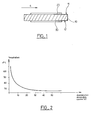
- the treatment method in accordance with the present invention firstly consists in depositing a coating 20 to be treated, containing electrically conductive charges, on a first main face 11 of a dielectric support 10, and depositing a layer of an electrically conductive material 30 on a second main face 12 of the dielectric support 10.
- the second face of the dielectric support referenced 12 is opposite to the first face 11 and generally parallel to the latter.
- the aforementioned faces 11 and 12 are flat. Note however that the present invention is also likely to find application in the case of dielectric supports having main surfaces curved in one direction and allowing the application of microwave energy so that the vibration direction of the electric field is substantially parallel auxcoating 10 and layer 30 above.
- the deposition of the layer 30 of conductive material on the second face of the support 10 can be carried out using various techniques.
- the deposition of the layer 30 can also be carried out by simply placing the second face 12 of the dielectric support 10 on a metallic element.
- the Applicant has obtained excellent results by placing the support 10 on a metal cradle a few microns thick, the edges of which have been curved to avoid the appearance of discharges during the subsequent application of microwave energy.
- the assembly thus formed consisting of a dielectric support 10 covered on the one hand with a coating 20 to be treated, on the other hand with a layer 30 of electrically conductive material, is then subjected to the application of microwave energy. .
- This application is carried out so that the direction of vibration of the electric field is substantially parallel to the coating 20 and to the layer 30 of conductive material, as shown schematically by the arrow referenced E in FIG. 1.
- the above-mentioned assembly can for example be deposited in the plane of symmetry of a waveguide, where the electric field is maximum.
- microwave energy applicators may be used for the implementation of the present invention. These arrangements which are well known to those skilled in the art will not be described below.
- the intensity of the electric field is reinforced in the plane of the second face (carrying the layer of electrically conductive material) at the expense of the intensity on the first face (carrying the coating to be treated). Therefore, the heating of the dielectric loss support is increased and the coating processing speed is reduced.
- the intensified electric field applied to the second face of the support heats the layer of electrically conductive material, by loss of conduction, the heat thus produced being transmitted to the dielectric support.
- the Applicant has measured the temperature reached, under the action of microwaves, by an epoxy glass-paper-support, with a thickness of 0.9 mm, the surface 12 opposite to that receiving the coating to be treated 20 is placed on a silver washer with a diameter of 26 mm.
- the tests were carried out for an applied power of around 1 kW and with a frequency of 2.45 GHz.
- the tests were carried out with silver washers of variable thickness, in order to control the influence of this parameter on the heating of the support.
- the crosslinking speed of the conductive ink could be easily controlled so that the product was perfectly crosslinked in times of 7 to 10 minutes.
- thermal treatment process by applying microwaves, of coatings containing electrically conductive charges on metallized dielectric supports, before treatment, opposite to the coating, is capable of very numerous applications, in particular in composite electronic components industry, for example for the production of keyboards.
- the metallization layer deposited on the second face 12 of the support can be removed to possibly allow subsequent deposition of other products.
- the frequency range of the microwaves used is between approximately 0.1 GHz and approximately 100 GHz, preferably between approximately 0.5 GHz and approximately 30 GHz, the penetration depth of the microwaves being a few microns for metals.
Landscapes
- Engineering & Computer Science (AREA)
- Physics & Mathematics (AREA)
- Electromagnetism (AREA)
- Manufacturing & Machinery (AREA)
- Microelectronics & Electronic Packaging (AREA)
- Constitution Of High-Frequency Heating (AREA)
- Thermal Transfer Or Thermal Recording In General (AREA)
- Laminated Bodies (AREA)
- Non-Insulated Conductors (AREA)
- Manufacturing Of Electric Cables (AREA)
Applications Claiming Priority (2)
| Application Number | Priority Date | Filing Date | Title |
|---|---|---|---|
| FR8314989A FR2552293B1 (fr) | 1983-09-21 | 1983-09-21 | Procede de traitement thermique, par application d'energie micro-onde, de revetements sur supports dielectriques, en particulier de revetements electriquement conducteurs, et produits obtenus |
| FR8314989 | 1983-09-21 |
Publications (3)
| Publication Number | Publication Date |
|---|---|
| EP0140746A2 true EP0140746A2 (de) | 1985-05-08 |
| EP0140746A3 EP0140746A3 (en) | 1985-07-10 |
| EP0140746B1 EP0140746B1 (de) | 1987-08-12 |
Family
ID=9292396
Family Applications (1)
| Application Number | Title | Priority Date | Filing Date |
|---|---|---|---|
| EP19840401856 Expired EP0140746B1 (de) | 1983-09-21 | 1984-09-19 | Verfahren zur Hitzebehandlung von elektrischleitenden Beschichtungen auf dielektrischen Trägern mittels Mikrowellen |
Country Status (5)
| Country | Link |
|---|---|
| US (1) | US4585699A (de) |
| EP (1) | EP0140746B1 (de) |
| JP (1) | JPS6134888A (de) |
| DE (1) | DE3465258D1 (de) |
| FR (1) | FR2552293B1 (de) |
Families Citing this family (5)
| Publication number | Priority date | Publication date | Assignee | Title |
|---|---|---|---|---|
| US5538754A (en) * | 1991-03-26 | 1996-07-23 | Shipley Company Inc. | Process for applying fluid on discrete substrates |
| US5262207A (en) * | 1991-09-03 | 1993-11-16 | General Motors Corporation | Method of electrostatically coating nonconductive panels |
| US7547647B2 (en) * | 2004-07-06 | 2009-06-16 | Hewlett-Packard Development Company, L.P. | Method of making a structure |
| WO2007038950A1 (en) * | 2005-09-28 | 2007-04-12 | Stichting Dutch Polymer Institute | Method for generation of metal surface structures and apparatus therefor |
| EP2194764A1 (de) * | 2008-12-04 | 2010-06-09 | Stichting Dutch Polymer Institute | Verfahren zur Erzeugung von elektrisch leitenden Oberflächenstrukturen, Vorrichtung und Verwendung dafür |
Family Cites Families (4)
| Publication number | Priority date | Publication date | Assignee | Title |
|---|---|---|---|---|
| FR1473832A (fr) * | 1963-09-09 | 1967-03-24 | Atlas Werke Ag | Dispositif générateur de chaleur à partir d'énergie de micro-ondes, notamment pour la décongélation de produits alimentaires |
| US3705819A (en) * | 1967-12-15 | 1972-12-12 | Heller William C Jun | Drying by induction heating |
| FR2078880A5 (de) * | 1970-02-23 | 1971-11-05 | Fuji Photo Film Co Ltd | |
| FR2458323A1 (fr) * | 1979-06-08 | 1981-01-02 | Anvar | Procede et appareil pour le traitement par micro-ondes de revetements sur substrats |
-
1983
- 1983-09-21 FR FR8314989A patent/FR2552293B1/fr not_active Expired
-
1984
- 1984-09-18 US US06/651,834 patent/US4585699A/en not_active Expired - Fee Related
- 1984-09-19 DE DE8484401856T patent/DE3465258D1/de not_active Expired
- 1984-09-19 EP EP19840401856 patent/EP0140746B1/de not_active Expired
- 1984-09-21 JP JP19933984A patent/JPS6134888A/ja active Pending
Also Published As
| Publication number | Publication date |
|---|---|
| DE3465258D1 (en) | 1987-09-17 |
| JPS6134888A (ja) | 1986-02-19 |
| EP0140746B1 (de) | 1987-08-12 |
| FR2552293B1 (fr) | 1986-04-11 |
| FR2552293A1 (fr) | 1985-03-22 |
| US4585699A (en) | 1986-04-29 |
| EP0140746A3 (en) | 1985-07-10 |
Similar Documents
| Publication | Publication Date | Title |
|---|---|---|
| EP0428458B1 (de) | Mehrschichtmaterial, das weichen Graphit enthält und das mit einem Metall mechanisch, elektrisch und thermisch verstärkt ist und das Verfahren zu seiner Herstellung | |
| FR2629978A1 (fr) | Circuit de protection ou de blindage contre les ondes electromagnetiques et son procede de fabrication | |
| FR2722330A1 (fr) | Cable coaxial | |
| FR2913972A1 (fr) | Procede de fabrication d'un masque pour la realisation d'une grille | |
| WO2016120302A1 (fr) | Dispositif chauffant, en particulier semi-transparent | |
| CA2712381C (fr) | Procede de fabrication d'un element chauffant par depot de couches minces sur un substrat isolant, et l'element obtenu | |
| EP3465748B1 (de) | Verfahren zur verarbeitung eines elektrisch isolierenden materials für elektrische komponenten, nach diesem verfahren hergestelltes elektrisches komponent und vorrichtung zur verarbeitung eines elektrisch isolierenden materials | |
| EP0140746B1 (de) | Verfahren zur Hitzebehandlung von elektrischleitenden Beschichtungen auf dielektrischen Trägern mittels Mikrowellen | |
| JP2002505803A (ja) | パリレンコーティングの製造方法 | |
| WO2000053823A1 (fr) | Procede de traitement de surface des polymeres | |
| EP0533575A1 (de) | Durch Metallisierung-Platierung auf Plastikoberflächen hergestellte Metallbänder | |
| FR2617325A1 (fr) | Cable electrique, notamment pour aeronef | |
| EP0539260B1 (de) | Verfahren zur Metallisieren von Werkstücken aus Kunststoff | |
| FR2655180A1 (fr) | Materiau magnetique composite en feuilles et son procede de fabrication. | |
| EP1070971A1 (de) | Verfahren zur Oberflächenbehandlung von optischen Fahrzeugbauteilen aus Kunststoff | |
| EP0061374B1 (de) | Verfahren zur Herstellung eines piezoelektrischen Verbundmaterials | |
| EP1603376A1 (de) | Leiterplatte durch selektive Beschichtung | |
| FR3074087A1 (fr) | Procede pour fabriquer un objet thermoforme metallise | |
| FR2989007A1 (fr) | Procede de metallisation d'une patte de connexion d'un composant electrique | |
| EP0418148B1 (de) | Verfahren zur Herstellung eines metallisierten Trägers auf Basis von Polymethylpenten | |
| EP0545748B1 (de) | Anordnung zur Zuführung einer Spannung auf einen Substrathalter | |
| EP1448805A2 (de) | Verbessertes verfahren zum beschichten eines trägers mit einem material | |
| FR2691170A3 (fr) | Procédé de traitement de surface de matériaux isolants. | |
| EP2212900A1 (de) | Verfahren und vorrichtung zur herstellung eines gleichmässigen ablaufs für nicht isolierende substrate | |
| EP0700058B1 (de) | Verfahren zum Schutz von porösen Bauelementen vor hohen Potentialdifferenzen und danach hergestellte Bauelemente |
Legal Events
| Date | Code | Title | Description |
|---|---|---|---|
| PUAI | Public reference made under article 153(3) epc to a published international application that has entered the european phase |
Free format text: ORIGINAL CODE: 0009012 |
|
| AK | Designated contracting states |
Designated state(s): DE GB |
|
| PUAL | Search report despatched |
Free format text: ORIGINAL CODE: 0009013 |
|
| AK | Designated contracting states |
Designated state(s): DE GB |
|
| 17P | Request for examination filed |
Effective date: 19851125 |
|
| 17Q | First examination report despatched |
Effective date: 19860418 |
|
| RAP1 | Party data changed (applicant data changed or rights of an application transferred) |
Owner name: CENTRE NATIONAL DE LA RECHERCHE SCIENTIFIQUE (CNRS |
|
| GRAA | (expected) grant |
Free format text: ORIGINAL CODE: 0009210 |
|
| AK | Designated contracting states |
Kind code of ref document: B1 Designated state(s): DE GB |
|
| REF | Corresponds to: |
Ref document number: 3465258 Country of ref document: DE Date of ref document: 19870917 |
|
| PLBE | No opposition filed within time limit |
Free format text: ORIGINAL CODE: 0009261 |
|
| STAA | Information on the status of an ep patent application or granted ep patent |
Free format text: STATUS: NO OPPOSITION FILED WITHIN TIME LIMIT |
|
| 26N | No opposition filed | ||
| PGFP | Annual fee paid to national office [announced via postgrant information from national office to epo] |
Ref country code: GB Payment date: 19940913 Year of fee payment: 11 |
|
| PGFP | Annual fee paid to national office [announced via postgrant information from national office to epo] |
Ref country code: DE Payment date: 19940923 Year of fee payment: 11 |
|
| PG25 | Lapsed in a contracting state [announced via postgrant information from national office to epo] |
Ref country code: GB Effective date: 19950919 |
|
| GBPC | Gb: european patent ceased through non-payment of renewal fee |
Effective date: 19950919 |
|
| PG25 | Lapsed in a contracting state [announced via postgrant information from national office to epo] |
Ref country code: DE Effective date: 19960601 |