EP0140809A1 - Vorrichtung zur Echokorrektur, insbesondere für ein Fernseh-Datenübertragungssystem - Google Patents
Vorrichtung zur Echokorrektur, insbesondere für ein Fernseh-Datenübertragungssystem Download PDFInfo
- Publication number
- EP0140809A1 EP0140809A1 EP84460007A EP84460007A EP0140809A1 EP 0140809 A1 EP0140809 A1 EP 0140809A1 EP 84460007 A EP84460007 A EP 84460007A EP 84460007 A EP84460007 A EP 84460007A EP 0140809 A1 EP0140809 A1 EP 0140809A1
- Authority
- EP
- European Patent Office
- Prior art keywords
- output
- input
- transversal filter
- coefficients
- analog
- Prior art date
- Legal status (The legal status is an assumption and is not a legal conclusion. Google has not performed a legal analysis and makes no representation as to the accuracy of the status listed.)
- Granted
Links
Images
Classifications
-
- H—ELECTRICITY
- H04—ELECTRIC COMMUNICATION TECHNIQUE
- H04B—TRANSMISSION
- H04B3/00—Line transmission systems
- H04B3/02—Details
- H04B3/20—Reducing echo effects or singing; Opening or closing transmitting path; Conditioning for transmission in one direction or the other
- H04B3/23—Reducing echo effects or singing; Opening or closing transmitting path; Conditioning for transmission in one direction or the other using a replica of transmitted signal in the time domain, e.g. echo cancellers
-
- H—ELECTRICITY
- H04—ELECTRIC COMMUNICATION TECHNIQUE
- H04B—TRANSMISSION
- H04B3/00—Line transmission systems
- H04B3/02—Details
- H04B3/20—Reducing echo effects or singing; Opening or closing transmitting path; Conditioning for transmission in one direction or the other
- H04B3/23—Reducing echo effects or singing; Opening or closing transmitting path; Conditioning for transmission in one direction or the other using a replica of transmitted signal in the time domain, e.g. echo cancellers
- H04B3/238—Reducing echo effects or singing; Opening or closing transmitting path; Conditioning for transmission in one direction or the other using a replica of transmitted signal in the time domain, e.g. echo cancellers using initial training sequence
Definitions
- the present invention relates to an echo correction device in digital transmission, that is to say interference correction between symbols, the correction being carried out on the received demodulated analog signal. More particularly, the invention relates to an echo correction device intervening in a data broadcasting system, such as that which is described in patent FR-2 313 825 and which is implemented under the name of "DIDON network "by the public broadcasting establishment known as” Telecommunicationdiffusion de France ".
- the DIDON network binary data is transmitted in amplitude modulation in NRZ code in packets on television image lines broadcast in particular by radio channels and the bit frequency is 6.2 MHz.
- the broadcasting channel brings a number of disturbances to the video signal, such as selective fading, noise and echoes resulting from reflections close to the reception site.
- the impulse response is therefore distorted and, given the high bit frequency which is used, this results in a phenomenon of overlapping of the pulses, that is to say a phenomenon of interference between symbols.
- the phenomena of echoes increase the sensitivity of the signal to noise and noise, it is important to provide an echo corrector in the DIDON network data receivers.
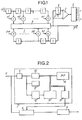
- Fig. 1 shows the diagram of a linear self-adjusting corrector of a known type which comprises, on the one hand, a recursive transversal filter 1 and, on the other hand, a calculation circuit 2, 3 and 4.
- the filter 1 is similar to that shown in FIG. A.2. from page 489 of the already cited work.
- the signal to be corrected x (t) is applied to the input of a first chain of r cells connected in series and each providing a delay equal to T where T is the inverse of the bit frequency.
- the outputs of the r cells are connected to the first inputs of r multipliers whose multiplication coefficients are respectively al to ar.
- the outputs of the r multipliers are connected to corresponding inputs of a summator S.
- the output of the summator S which delivers the corrected signal y (t), is also connected to a chain of m cells connected in series and each providing a delay T.
- the outputs of the m cells are connected to the inputs of m multipliers whose multiplier coefficients are respectively bl to bm.
- the outputs of the m multipliers are connected to corresponding inputs of the summator S.
- the calculation circuit 2 delivers the coefficients al to ar and bl to bm which are applied, in filter 1, to the corresponding inputs of the multipliers.
- the input of the calculation circuit 2 is connected to the output of a comparator 3, one input of which is connected directly to the output of the filter 1 and the other input of which is connected to the output of a threshold detector 4, the l the signal input is also connected to the output of the filter 1.
- the threshold detector 4 has a control input 5 to which a reference voltage defining the thresholds is applied.
- the filter 1 is a direct and non-recursive filter, which amounts to canceling the coefficients bl to bm.
- the threshold detector 4 is added in the recursive part. If a reference signal is directly applied to the second input of comparator 3, the filter then being only adaptive instead of being self-adaptive.
- the reference voltage applied to the control input 5 of the threshold detector 4 is generally equal to the average value of the amplitude of the output signal of the filter 1.
- the output signal of the threshold detector 4 therefore corresponds to a value estimated (t) of the output signal y (t).
- the correcting criterion is that of the mean square error: where a k is the transmitted signal, which is replaced by an estimated value in the case of a self-adaptive filter. In an autoadaptive filter, one seeks the coefficients composing the vector H which minimize this expression.
- An object of the invention is to provide a correction device comprising an analog linear filter whose coefficients can be determined by applying digital calculation techniques.
- a correction device comprising an analog transverse filter and a calculation circuit delivering the coefficients al to ar and, optionally, bl to bm of the analog transversal filter, the input of the calculation circuit being connected to the input of the analog transversal filter and the calculation circuit comprising an analog / digital converter whose output is connected to a self-adapting digital transversal filter, some, at least, of the coefficients of the multipliers of the digital transversal filter being applied to the multipliers of the analog cross filter.
- the analog transversal filter is of the same type as the digital transversal filter.
- the optimization criterion is that of the mean square error and the convergence algorithm is that of the gradient, the iterative correction being carried out at each step on the set of coefficients of the filter.
- the optimization criterion is that of the mean square error and the convergence algorithm is that of the gradient, the iterative correction being cyclically performed on each of the coefficients.
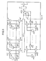
- the video signal carrying the data is applied to the input E which is connected in parallel, on the one hand, to a transverse filter 6 and, on the other hand, to a calculation circuit 7.
- the filter 6 operates directly on the analog signal applied to the input El and delivers a corrected analog signal which is applied to a DIDON 8 demodulator which is preferably of the type of receiver described in patent FR-2 313 825.
- the calculation circuit 7 comprises a clamping circuit 9, the output of which is connected in parallel to a mean value calculation circuit 10, a synchronization circuit 11 and to an analog-digital converter 12, the output of which is connected to a memory 13
- the calculation circuit 7 also comprises a microprocessor 14.
- the software of the microprocessor 14 is provided so that the calculation circuit 7 functions, for example, as a recursive self-adapting transverse filter with decision in the loop.
- the sampling frequency is equal to the bit frequency, the sampling instant being centered in each elementary time.
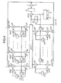
- the diagram in FIG. 3 symbolizes the filter constituted by the calculation circuit 7.
- the samples X (t), coming from the analog-digital converter 12, are applied to the input of a chain of 1 registers RD1 to RD1.
- the outputs of registers RD1 to RD1 are respectively connected to the first inputs of 1 digital multipliers Al to Al whose outputs are connected to the first 1 inputs of a digital summator SOM1.
- the registers RD1 to RD1 can operate in shift register with a clock of period T.
- the output of the summator SOM1 is connected, on the one hand, to the input of a threshold detector DS and, on the other hand, to the input - of a summator SOM2 whose input + is connected to the DS detector output.
- the output of the detector DS is connected to the input of a chain of p shift registers RR1 to RRp.
- the outputs of the registers RR1 to RRp are respectively connected to the first inputs of p multipliers B1 to B1 whose outputs are connected to p inputs of the summator SOM1.
- the registers RR1 to RR1 can form a shift register with a clock of period T.
- the input for controlling the threshold level in the detector DS is connected to the output of the average value calculation circuit 10.
- the elements of the diagram in FIG. 3 which have just been described constitute a part of a recursive transverse digital filter with decision in the loop.
- the other part of the filter must include a circuit for calculating the coefficients of the multipliers Al to Al and Bl to Bp. We will now describe this calculation circuit.
- the output of the summator SOM2 is connected to an estimation circuit CE, the output of which is connected to a multiplier C at the second input from which the value of a coefficient u is applied.
- the output of the multiplier C is connected to the first inputs of a first series of multipliers Dl to Dl and of a second series of multipliers El to Ep.
- the second inputs of the multipliers Dl to Dl are respectively connected to the outputs of the registers RD1 to RD1 .
- the second inputs of multipliers El to Ep are respectively connected to the outputs of registers RR1 to RRp.
- the outputs of the multipliers Dl to Dl are respectively connected to the inputs - of summers ADD1 to ADDl whose outputs are respectively connected, on the one hand, to the second inputs of the multipliers A1 to Al and, on the other hand, to the memory inputs MD1 to MD1.
- the outputs of memories MD1 to MD1 are respectively connected to the inputs + of summers ADD1 to ADD1.
- the outputs of the multipliers El to Ep are respectively connected to the inputs - of summers ADR1 to ADRp whose outputs are respectively connected, on the one hand, to the second inputs of the multipliers B1 to Bp and, on the other hand, to the memory inputs MR1 at MRp.
- the outputs of memories MR1 to MRp are respectively connected to the inputs + of summers ADR1 to ADRp.
- the memories MD1 to MD1 present at their outputs, at the sampling instant k, the values H1 k to Hl k which have been written there at the sampling instant (k-1). Under the same conditions, the memories MR1 to MRp deliver the values Jl k to J p k .
- the output signal from the summator SOM2 corresponds to the difference e between the estimated signal a k delivered by the detector DS and the output signal y k from the summator SOM1.
- the indices k indicate the rank of the digital samples considered.
- the signal e is therefore an error signal which is processed in the estimation circuit CE.
- the quadratic mean error is used as the optimization criterion for the corrector. If F (H) represents the mean square error, we have: where the vector H is the vector corresponding to the coefficients Hl to Hl.
- the algorithm chosen to minimize the criterion F (H) is, in an exemplary embodiment according to the invention, the gradient algorithm which is defined below.
- the first member of the equal The above is a positive quantity.
- the second member being the scalar product of two vectors, it is necessary that is of opposite direction to ⁇ .F ( H k ) and that it be parallel to it to increase this scalar product, which implies: Is:
- the convergence step of the algorithm is a constant value u which is chosen to be close to the value ⁇ defined above.
- the circuit CE is designed to deliver the signal sg (e k ). We therefore have, on the first inputs of the multipliers Dl to Dl, the signal u.sg (e k ) and, like the second inputs of the summers ADD1 to ADDl form the components of the vector H k , we have at the output of the same summers the components of the vector H k + 1 .
- the different operations - additions, multiplications, delays - which are carried out by the corresponding elements - summers, multipliers, registers - shown in FIG. 3 can also be carried out using appropriate software of the microprocessor 14 of FIG. 2. Indeed, all the samples X k , Y k , H1 k to Hl k , il k to Jp are available in memory 13, which also contains the value of u and possibly of u '. Finally, for the operation of the threshold decision circuit DS, the mean value calculation circuit 9 periodically supplies this value which is also stored in memory 13.
- the calculation circuit 7 of FIG. 2 also includes a buffer register 15 in which the vector coefficients are stored H k , that is to say the output coefficients of the memories MD1 to MD1.
- the outputs of the buffer register are respectively connected to control inputs of the analog linear filter 6, these control inputs delivering the coefficients of the multipliers of the filter 6.
- the filter 6 can be constituted by a series of delay cells, each cell providing a delay T.
- an analog multiplier circuit is inserted, an input of which is connected at the end of the length of upstream cable and the outlet at the input of the downstream cable length.
- the other input of the multiplier is connected to the output of a digital-analog converter whose digital input is connected to the corresponding output of the buffer register 15.
- the content of the buffer register 15 is refreshed only periodically, for example every ten seconds. After each new loading of the register 15, the coefficients already calculated are kept in the memory 13. On the other hand, the samples present in this memory are replaced by the new incoming samples.
- one of the coefficients Hl to Hl takes the value 1 while the other coefficients are zero, as well as the coefficients J1 to Jp.
- the rank of the coefficient initially set to 1 defines what is known as the central coefficient. The choice of the central coefficient makes it possible to define the maximum temporal deviation of the echoes that the filter can correct.
Landscapes
- Computer Networks & Wireless Communication (AREA)
- Signal Processing (AREA)
- Engineering & Computer Science (AREA)
- Filters That Use Time-Delay Elements (AREA)
- Cable Transmission Systems, Equalization Of Radio And Reduction Of Echo (AREA)
- Details Of Television Systems (AREA)
- Two-Way Televisions, Distribution Of Moving Picture Or The Like (AREA)
- Primary Cells (AREA)
- Structure Of Transmissions (AREA)
- Curing Cements, Concrete, And Artificial Stone (AREA)
- On-Site Construction Work That Accompanies The Preparation And Application Of Concrete (AREA)
- Ultra Sonic Daignosis Equipment (AREA)
- Radar Systems Or Details Thereof (AREA)
- Input Circuits Of Receivers And Coupling Of Receivers And Audio Equipment (AREA)
- Numerical Control (AREA)
Priority Applications (1)
| Application Number | Priority Date | Filing Date | Title |
|---|---|---|---|
| AT84460007T ATE34495T1 (de) | 1983-10-28 | 1984-10-09 | Vorrichtung zur echokorrektur, insbesondere fuer ein fernseh-datenuebertragungssystem. |
Applications Claiming Priority (2)
| Application Number | Priority Date | Filing Date | Title |
|---|---|---|---|
| FR8317438A FR2556530B1 (fr) | 1983-10-28 | 1983-10-28 | Dispositif de correction d'echos, notamment pour systeme de diffusion de donnees |
| FR8317438 | 1983-10-28 |
Publications (2)
| Publication Number | Publication Date |
|---|---|
| EP0140809A1 true EP0140809A1 (de) | 1985-05-08 |
| EP0140809B1 EP0140809B1 (de) | 1988-05-18 |
Family
ID=9293722
Family Applications (1)
| Application Number | Title | Priority Date | Filing Date |
|---|---|---|---|
| EP84460007A Expired EP0140809B1 (de) | 1983-10-28 | 1984-10-09 | Vorrichtung zur Echokorrektur, insbesondere für ein Fernseh-Datenübertragungssystem |
Country Status (12)
| Country | Link |
|---|---|
| US (1) | US4696015A (de) |
| EP (1) | EP0140809B1 (de) |
| JP (1) | JPS60111537A (de) |
| AT (1) | ATE34495T1 (de) |
| AU (1) | AU566962B2 (de) |
| BR (1) | BR8405550A (de) |
| CA (1) | CA1217856A (de) |
| DE (1) | DE3471414D1 (de) |
| ES (1) | ES8507300A1 (de) |
| FR (1) | FR2556530B1 (de) |
| MX (1) | MX155974A (de) |
| PT (1) | PT79396B (de) |
Cited By (1)
| Publication number | Priority date | Publication date | Assignee | Title |
|---|---|---|---|---|
| EP0409756A1 (de) * | 1989-07-18 | 1991-01-23 | France Telecom | Datenempfangsanlage mit verzögerter Entzerrung und retroaktiver Taktwiedergewinnung |
Families Citing this family (13)
| Publication number | Priority date | Publication date | Assignee | Title |
|---|---|---|---|---|
| US4811261A (en) * | 1985-03-04 | 1989-03-07 | Oki Electric Industry Co., Ltd. | Adaptive digital filter for determining a transfer equation of an unknown system |
| ATE62365T1 (de) * | 1986-01-30 | 1991-04-15 | Siemens Ag | Echokompensator. |
| US5058047A (en) * | 1989-05-30 | 1991-10-15 | Advanced Micro Devices, Inc. | System and method for providing digital filter coefficients |
| US5535150A (en) * | 1993-04-20 | 1996-07-09 | Massachusetts Institute Of Technology | Single chip adaptive filter utilizing updatable weighting techniques |
| US6542611B1 (en) * | 1998-07-31 | 2003-04-01 | Circuit Research Labs, Inc. | Multi-state echo suppressor |
| DE19925046A1 (de) * | 1999-06-01 | 2001-05-03 | Alcatel Sa | Verfahren und Vorrichtung zur Unterdrückung von Rauschen und Echos |
| US6480532B1 (en) * | 1999-07-13 | 2002-11-12 | Stmicroelectronics, Inc. | Echo cancellation for an ADSL modem |
| FR2801753B1 (fr) * | 1999-11-25 | 2002-05-03 | Groupe Ecoles Telecomm | Perfectionnements aux dispositifs d'egalisation adaptative pour recuperateurs de systemes de communication numeriques |
| US8295475B2 (en) * | 2006-01-13 | 2012-10-23 | Microsoft Corporation | Selective glitch detection, clock drift compensation, and anti-clipping in audio echo cancellation |
| US7773743B2 (en) * | 2006-04-28 | 2010-08-10 | Microsoft Corporation | Integration of a microphone array with acoustic echo cancellation and residual echo suppression |
| US7831035B2 (en) * | 2006-04-28 | 2010-11-09 | Microsoft Corporation | Integration of a microphone array with acoustic echo cancellation and center clipping |
| US8380253B2 (en) | 2008-02-15 | 2013-02-19 | Microsoft Corporation | Voice switching for voice communication on computers |
| US8369251B2 (en) * | 2008-06-20 | 2013-02-05 | Microsoft Corporation | Timestamp quality assessment for assuring acoustic echo canceller operability |
Citations (2)
| Publication number | Priority date | Publication date | Assignee | Title |
|---|---|---|---|---|
| US3787645A (en) * | 1971-05-19 | 1974-01-22 | Nippon Electric Co | Echo canceller having two echo path models |
| EP0052362A1 (de) * | 1980-11-17 | 1982-05-26 | Nec Corporation | System für die schnelle Voreinstellung von Transversalentzerrern |
Family Cites Families (7)
| Publication number | Priority date | Publication date | Assignee | Title |
|---|---|---|---|---|
| NL171215C (nl) * | 1973-03-09 | 1983-02-16 | Trt Telecom Radio Electr | Automatische egalisatie-inrichting voor een datatransmissiekanaal. |
| FR2370396A1 (fr) * | 1976-11-09 | 1978-06-02 | Cit Alcatel | Ensemble d'egalisation autoadaptatif |
| FR2410917A1 (fr) * | 1977-11-30 | 1979-06-29 | Cit Alcatel | Egaliseur autoadaptatif |
| US4321686A (en) * | 1980-01-24 | 1982-03-23 | Communications Satellite Corporation | Correction processor of self-adaptive filters |
| FR2479617A1 (fr) * | 1980-03-26 | 1981-10-02 | Trt Telecom Radio Electr | Annuleur d'echo pour signal d'echo a phase variable |
| JPS56169919A (en) * | 1980-06-03 | 1981-12-26 | Toshiba Corp | Automatic equalizer |
| FR2541837A1 (fr) * | 1983-02-25 | 1984-08-31 | Trt Telecom Radio Electr | Procede de reduction du temps de convergence d'un annuleur d'echo et dispositif pour mettre en oeuvre ce procede |
-
1983
- 1983-10-28 FR FR8317438A patent/FR2556530B1/fr not_active Expired
-
1984
- 1984-10-09 EP EP84460007A patent/EP0140809B1/de not_active Expired
- 1984-10-09 DE DE8484460007T patent/DE3471414D1/de not_active Expired
- 1984-10-09 AT AT84460007T patent/ATE34495T1/de active
- 1984-10-19 US US06/662,961 patent/US4696015A/en not_active Expired - Fee Related
- 1984-10-19 CA CA000465957A patent/CA1217856A/en not_active Expired
- 1984-10-24 PT PT79396A patent/PT79396B/pt unknown
- 1984-10-26 ES ES537153A patent/ES8507300A1/es not_active Expired
- 1984-10-26 BR BR8405550A patent/BR8405550A/pt unknown
- 1984-10-26 AU AU34756/84A patent/AU566962B2/en not_active Ceased
- 1984-10-26 MX MX203190A patent/MX155974A/es unknown
- 1984-10-29 JP JP59225996A patent/JPS60111537A/ja active Pending
Patent Citations (2)
| Publication number | Priority date | Publication date | Assignee | Title |
|---|---|---|---|---|
| US3787645A (en) * | 1971-05-19 | 1974-01-22 | Nippon Electric Co | Echo canceller having two echo path models |
| EP0052362A1 (de) * | 1980-11-17 | 1982-05-26 | Nec Corporation | System für die schnelle Voreinstellung von Transversalentzerrern |
Non-Patent Citations (3)
| Title |
|---|
| IEEE TRANSACTIONS ON CONSUMER ELECTRONICS, vol. CE-27, no. 3, août 1981, pages 512-529, New York, US; J.O. VOORMAN et al.: "A one-chip automatic equalizer for echo reduction in teletext" * |
| IEEE TRANSACTIONS ON CONSUMER ELECTRONICS, vol. CE-28, no. 3, août 1982, pages 447-452, New York, US; M. OBARA et al.: "A digital time domain equalizer for teletext" * |
| NATIONAL TELECOMMUNICATIONS CONFERENCE, Houston, 30 novembre - 4 décembre 1980, vol. 3, pages 56.4.1 - 56.4.4, IEEE, New York, US; E.J. McDEVITT: "A microprocessor based adaptive digital echo canceller" * |
Cited By (2)
| Publication number | Priority date | Publication date | Assignee | Title |
|---|---|---|---|---|
| EP0409756A1 (de) * | 1989-07-18 | 1991-01-23 | France Telecom | Datenempfangsanlage mit verzögerter Entzerrung und retroaktiver Taktwiedergewinnung |
| FR2650137A1 (de) * | 1989-07-18 | 1991-01-25 | France Etat |
Also Published As
| Publication number | Publication date |
|---|---|
| BR8405550A (pt) | 1985-09-10 |
| DE3471414D1 (en) | 1988-06-23 |
| MX155974A (es) | 1988-06-03 |
| US4696015A (en) | 1987-09-22 |
| AU566962B2 (en) | 1987-11-05 |
| CA1217856A (en) | 1987-02-10 |
| EP0140809B1 (de) | 1988-05-18 |
| AU3475684A (en) | 1985-05-09 |
| FR2556530B1 (fr) | 1986-04-04 |
| PT79396B (fr) | 1986-07-22 |
| JPS60111537A (ja) | 1985-06-18 |
| ES537153A0 (es) | 1985-08-16 |
| FR2556530A1 (fr) | 1985-06-14 |
| PT79396A (fr) | 1984-11-01 |
| ATE34495T1 (de) | 1988-06-15 |
| ES8507300A1 (es) | 1985-08-16 |
Similar Documents
| Publication | Publication Date | Title |
|---|---|---|
| EP0140809B1 (de) | Vorrichtung zur Echokorrektur, insbesondere für ein Fernseh-Datenübertragungssystem | |
| EP0576359B1 (de) | Verfahren und Einrichtung zur entscheidungsrückgekoppelten Entzerrung für die blockweise Übertragung von Informationssymbolen | |
| EP0146979A1 (de) | Verfahren und Einrichtung zur Bestimmung der optimalen Lage des Referenzkoeffizienten eines adaptiven Entzerrers | |
| EP0174678B1 (de) | Echokompensator mit Anwendung der delta-Modulation | |
| EP0692883B1 (de) | Verfahren zur blinden Entzerrung, und dessen Anwendung zur Spracherkennung | |
| EP0039980B1 (de) | Adaptives digitales Datenempfangssystem mit Kompensation der durch den Datenübertragungskanal verursachten Amplituden- und Phasenverzerrungen | |
| EP0970562B1 (de) | Digitalfilter für fraktionale verzögerungen | |
| EP0127544B1 (de) | Echokompensator mit einem adaptiven digitalen Filter für ein Übertragungssystem | |
| EP1113634A1 (de) | Verfahren zur Übertragungskanalschätzung | |
| EP0511698B1 (de) | Halbrekursiver adaptiver Entzerrer | |
| EP0632589B1 (de) | Verfahren zur Berechnung von Wiegekoeffizienten eines analytischen Digitalisiergerätes für Signalverarbeitung und analytisches Digitalisiergerät | |
| EP0702467B1 (de) | Mittels Initialisierungsfolge synchronisierbares digitales Übertragungssystem | |
| EP0528738B1 (de) | Verfahren und Schaltung zur Koeffizientenanpassung im Entzerrer eines Modems | |
| EP1478096B1 (de) | Selbstanpassende Vorrichtung und Verfahren zur Interferenz-Unterdruckung | |
| EP1438815A1 (de) | Zwischensymbolstörungslöscher | |
| EP1155497B1 (de) | System und verfahren zum verarbeiten von antennensignalen | |
| EP1206045A1 (de) | Verfahren zum Korrigieren der Frequenzfehler | |
| FR2711028A1 (fr) | Procédé et dispositif de démodulation cohérente par blocs de signaux complexes modulés en phase. | |
| EP0652663B1 (de) | Frequenzbereichsentzerrer | |
| EP0860963B1 (de) | Verfahren und Einrichtung zur automatischen Entzerrung eines Übertragungskanals, das Signale von wesentlich konstantem Betrag trägt | |
| EP0944211B1 (de) | Verfahren und Einrichting zur adaptiven, vorhersagenden Entzerrung eines Rundfunkübertragungskanal | |
| EP1826973A1 (de) | Verfahren und Gerät zur Schätzung der Übertragungsfunktions des Kanals für einen COFDM-Demodulator | |
| EP1826974A1 (de) | Verfahren und Gerät zur Schätzung der Kanalübertragungsfunktion für einen COFDM Demodulator | |
| CA2106702A1 (fr) | Dispositif de filtrage pour egaliseur a estimation de sequence | |
| FR2734433A1 (fr) | Procede et egaliseur adaptatif pour egaliser un signal numerique transmis par liaisons hertzienne |
Legal Events
| Date | Code | Title | Description |
|---|---|---|---|
| PUAI | Public reference made under article 153(3) epc to a published international application that has entered the european phase |
Free format text: ORIGINAL CODE: 0009012 |
|
| AK | Designated contracting states |
Designated state(s): AT BE CH DE GB IT LI LU NL SE |
|
| RTI1 | Title (correction) | ||
| 17P | Request for examination filed |
Effective date: 19851028 |
|
| 17Q | First examination report despatched |
Effective date: 19870408 |
|
| ITF | It: translation for a ep patent filed | ||
| GRAA | (expected) grant |
Free format text: ORIGINAL CODE: 0009210 |
|
| AK | Designated contracting states |
Kind code of ref document: B1 Designated state(s): AT BE CH DE GB IT LI LU NL SE |
|
| REF | Corresponds to: |
Ref document number: 34495 Country of ref document: AT Date of ref document: 19880615 Kind code of ref document: T |
|
| GBT | Gb: translation of ep patent filed (gb section 77(6)(a)/1977) | ||
| REF | Corresponds to: |
Ref document number: 3471414 Country of ref document: DE Date of ref document: 19880623 |
|
| PG25 | Lapsed in a contracting state [announced via postgrant information from national office to epo] |
Ref country code: LU Free format text: LAPSE BECAUSE OF NON-PAYMENT OF DUE FEES Effective date: 19881031 |
|
| PLBE | No opposition filed within time limit |
Free format text: ORIGINAL CODE: 0009261 |
|
| STAA | Information on the status of an ep patent application or granted ep patent |
Free format text: STATUS: NO OPPOSITION FILED WITHIN TIME LIMIT |
|
| 26N | No opposition filed | ||
| PG25 | Lapsed in a contracting state [announced via postgrant information from national office to epo] |
Ref country code: AT Effective date: 19891009 |
|
| PG25 | Lapsed in a contracting state [announced via postgrant information from national office to epo] |
Ref country code: BE Effective date: 19891031 |
|
| BERE | Be: lapsed |
Owner name: TELEDIFFUSION DE FRANCE Effective date: 19891031 |
|
| PGFP | Annual fee paid to national office [announced via postgrant information from national office to epo] |
Ref country code: GB Payment date: 19910814 Year of fee payment: 8 |
|
| PGFP | Annual fee paid to national office [announced via postgrant information from national office to epo] |
Ref country code: SE Payment date: 19910829 Year of fee payment: 8 |
|
| PGFP | Annual fee paid to national office [announced via postgrant information from national office to epo] |
Ref country code: CH Payment date: 19910917 Year of fee payment: 8 |
|
| ITTA | It: last paid annual fee | ||
| PGFP | Annual fee paid to national office [announced via postgrant information from national office to epo] |
Ref country code: NL Payment date: 19911031 Year of fee payment: 8 |
|
| PGFP | Annual fee paid to national office [announced via postgrant information from national office to epo] |
Ref country code: DE Payment date: 19911207 Year of fee payment: 8 |
|
| PG25 | Lapsed in a contracting state [announced via postgrant information from national office to epo] |
Ref country code: GB Effective date: 19921009 |
|
| PG25 | Lapsed in a contracting state [announced via postgrant information from national office to epo] |
Ref country code: SE Effective date: 19921010 |
|
| PG25 | Lapsed in a contracting state [announced via postgrant information from national office to epo] |
Ref country code: LI Effective date: 19921031 Ref country code: CH Effective date: 19921031 |
|
| PG25 | Lapsed in a contracting state [announced via postgrant information from national office to epo] |
Ref country code: NL Effective date: 19930501 |
|
| GBPC | Gb: european patent ceased through non-payment of renewal fee |
Effective date: 19921009 |
|
| NLV4 | Nl: lapsed or anulled due to non-payment of the annual fee | ||
| REG | Reference to a national code |
Ref country code: CH Ref legal event code: PL |
|
| PG25 | Lapsed in a contracting state [announced via postgrant information from national office to epo] |
Ref country code: DE Effective date: 19930701 |
|
| EUG | Se: european patent has lapsed |
Ref document number: 84460007.2 Effective date: 19930510 |