EP0141080A1 - Circuits d'évaluation pour des capteurs de mesure passifs - Google Patents
Circuits d'évaluation pour des capteurs de mesure passifs Download PDFInfo
- Publication number
- EP0141080A1 EP0141080A1 EP84109449A EP84109449A EP0141080A1 EP 0141080 A1 EP0141080 A1 EP 0141080A1 EP 84109449 A EP84109449 A EP 84109449A EP 84109449 A EP84109449 A EP 84109449A EP 0141080 A1 EP0141080 A1 EP 0141080A1
- Authority
- EP
- European Patent Office
- Prior art keywords
- transducer
- diagonal
- bridge circuit
- switch
- preamplifier
- Prior art date
- Legal status (The legal status is an assumption and is not a legal conclusion. Google has not performed a legal analysis and makes no representation as to the accuracy of the status listed.)
- Granted
Links
- 238000011156 evaluation Methods 0.000 title claims abstract description 30
- 238000005259 measurement Methods 0.000 claims description 21
- 230000005540 biological transmission Effects 0.000 claims description 9
- 238000000926 separation method Methods 0.000 claims description 7
- 230000004044 response Effects 0.000 claims description 6
- 230000000694 effects Effects 0.000 abstract description 4
- 235000002017 Zea mays subsp mays Nutrition 0.000 abstract description 3
- 241000482268 Zea mays subsp. mays Species 0.000 abstract description 3
- 230000008878 coupling Effects 0.000 description 6
- 238000010168 coupling process Methods 0.000 description 6
- 238000005859 coupling reaction Methods 0.000 description 6
- 230000003321 amplification Effects 0.000 description 5
- 238000003199 nucleic acid amplification method Methods 0.000 description 5
- 238000010586 diagram Methods 0.000 description 4
- 238000004804 winding Methods 0.000 description 4
- 238000000034 method Methods 0.000 description 3
- 230000008569 process Effects 0.000 description 3
- 239000004065 semiconductor Substances 0.000 description 3
- 101000968091 Pithecopus azureus Dermaseptin-H2 Proteins 0.000 description 2
- 101000927330 Pithecopus azureus Dermaseptin-H6 Proteins 0.000 description 2
- 230000008859 change Effects 0.000 description 2
- 230000001419 dependent effect Effects 0.000 description 2
- 230000007774 longterm Effects 0.000 description 2
- 230000001629 suppression Effects 0.000 description 2
- 230000001360 synchronised effect Effects 0.000 description 2
- 238000009966 trimming Methods 0.000 description 2
- 238000012935 Averaging Methods 0.000 description 1
- 108010014172 Factor V Proteins 0.000 description 1
- 239000003637 basic solution Substances 0.000 description 1
- 230000015572 biosynthetic process Effects 0.000 description 1
- 230000000903 blocking effect Effects 0.000 description 1
- 230000000295 complement effect Effects 0.000 description 1
- 238000010276 construction Methods 0.000 description 1
- 230000007547 defect Effects 0.000 description 1
- 230000007812 deficiency Effects 0.000 description 1
- 238000006073 displacement reaction Methods 0.000 description 1
- 238000005516 engineering process Methods 0.000 description 1
- 230000002349 favourable effect Effects 0.000 description 1
- 230000001939 inductive effect Effects 0.000 description 1
- 238000009434 installation Methods 0.000 description 1
- 230000010354 integration Effects 0.000 description 1
- 230000003993 interaction Effects 0.000 description 1
- 238000002955 isolation Methods 0.000 description 1
- 230000003252 repetitive effect Effects 0.000 description 1
- 230000000717 retained effect Effects 0.000 description 1
- 230000002441 reversible effect Effects 0.000 description 1
- 230000035945 sensitivity Effects 0.000 description 1
- 238000011144 upstream manufacturing Methods 0.000 description 1
Images





Classifications
-
- G—PHYSICS
- G01—MEASURING; TESTING
- G01D—MEASURING NOT SPECIALLY ADAPTED FOR A SPECIFIC VARIABLE; ARRANGEMENTS FOR MEASURING TWO OR MORE VARIABLES NOT COVERED IN A SINGLE OTHER SUBCLASS; TARIFF METERING APPARATUS; MEASURING OR TESTING NOT OTHERWISE PROVIDED FOR
- G01D5/00—Mechanical means for transferring the output of a sensing member; Means for converting the output of a sensing member to another variable where the form or nature of the sensing member does not constrain the means for converting; Transducers not specially adapted for a specific variable
- G01D5/12—Mechanical means for transferring the output of a sensing member; Means for converting the output of a sensing member to another variable where the form or nature of the sensing member does not constrain the means for converting; Transducers not specially adapted for a specific variable using electric or magnetic means
- G01D5/14—Mechanical means for transferring the output of a sensing member; Means for converting the output of a sensing member to another variable where the form or nature of the sensing member does not constrain the means for converting; Transducers not specially adapted for a specific variable using electric or magnetic means influencing the magnitude of a current or voltage
- G01D5/16—Mechanical means for transferring the output of a sensing member; Means for converting the output of a sensing member to another variable where the form or nature of the sensing member does not constrain the means for converting; Transducers not specially adapted for a specific variable using electric or magnetic means influencing the magnitude of a current or voltage by varying resistance
-
- G—PHYSICS
- G01—MEASURING; TESTING
- G01D—MEASURING NOT SPECIALLY ADAPTED FOR A SPECIFIC VARIABLE; ARRANGEMENTS FOR MEASURING TWO OR MORE VARIABLES NOT COVERED IN A SINGLE OTHER SUBCLASS; TARIFF METERING APPARATUS; MEASURING OR TESTING NOT OTHERWISE PROVIDED FOR
- G01D3/00—Indicating or recording apparatus with provision for the special purposes referred to in the subgroups
- G01D3/028—Indicating or recording apparatus with provision for the special purposes referred to in the subgroups mitigating undesired influences, e.g. temperature, pressure
- G01D3/036—Indicating or recording apparatus with provision for the special purposes referred to in the subgroups mitigating undesired influences, e.g. temperature, pressure on measuring arrangements themselves
-
- G—PHYSICS
- G01—MEASURING; TESTING
- G01R—MEASURING ELECTRIC VARIABLES; MEASURING MAGNETIC VARIABLES
- G01R17/00—Measuring arrangements involving comparison with a reference value, e.g. bridge
Definitions
- the invention relates to evaluation circuits for passive transducers with ohmic sensor resistances in bridge circuits with a comparison of the output signals of the transducers by permanently modulated switching of a resistor, which from the overflow signal of a clock pulse counter to a switchover position and from the output signal of a digital comparator of the contents of the clock pulse counter and one to the Output of a sign-sensitive voltage-frequency converter, the input voltage of which consists of an amplified adjustment difference signal rectified with a phase-sensitive rectifier and filtered by a low-pass filter, connected up-down counter to the other switching position, in which the transducers and the switchable resistance are controlled with a of Overflow of the clock pulse counter controlled pole switch are fed from a direct current or direct voltage source and the phase-sensitive rectifier synchronously with the pole switch holder is controlled.
- Such an evaluation circuit is known from DE-PS 22 62 755.
- the evaluation circuit called digital compensation device should be free from the effects of thermal voltages and contact potentials in the passive measured variable pickup and independent of the zero point drift of a so-called zero amplifier.
- a second contact of the changeover switch S2 is connected to a resistor R ', which alternates with the resistor R into the secondary circuit via the changeover switch
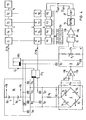
- the primary windings of the current transformers Tr1 and Tr2 are connected in series via a pole-changing switch S1 to a direct current source.
- the current IS flows in the primary windings.
- the difference between the voltages Um and Uk is fed to a switch S3 via lines L1 and L2 , which is connected upstream of a zero amplifier NV.
- a second pole changeover switch S4 is located at the output terminals of the zero amplifier. Its output terminals are connected to the input terminals of a voltage-frequency converter SPF via a low-pass filter TP.
- the pole changeover switch S4 is actuated synchronously with the pole changeover switch S1, so that it acts as a contact rectifier terminals of the voltage-frequency converter SPF are connected to the forward and reverse inputs of a pulse counter Z1.
- the counting input of a clock pulse counter Z2 is connected to the output of a clock generator, which delivers a pulse train with the repetition frequency f0.
- the decade outputs of the counters Z1 and Z2 are connected to comparison inputs of a digital comparison circuit DV.
- An output of the comparison circuit DV which carries a pulse k marking the correspondence of the counter contents z1 and z2, is at the input of a switch control logic Lo connected.
- a transmission pulse ü reaches a second input of the switching control logic Lo via a connecting line of the highest decade of the clock pulse counter Z2.
- a carry pulse v of a pre-clock counter VZ is fed to a further input of the switching control logic.
- An output of the switching control logic controls the two pole switches S1 and S4 simultaneously. Two further outputs of the switching control logic are used to control switches S2 and S3.
- the polarity of the supply voltage or the supply current is changed via the switching control logic Lo every time the clock pulse counter Z2 is counted up from the clock pulses of the clock pulse generator TG to its final counter value z2 max and emits a carry pulse u.
- the switch S2 is switched to the resistor R 'at the moment in which the clock pulse counter Z2 has the same content as the counter Z1 and the digital comparison circuit DV thus reports the coincidence of the counter contents to the switching control logic Lo with a pulse k .
- the arithmetic mean Uk of the compensation voltage Uk obtained in this way is thus directly proportional to the current counter content z1 of the counter Z1, based on the maximum counter content z2 max of the clock pulse counter Z2 .
- the interrupter switch S3 which is switched through by the switching control logic Lo at the same instant as the switch S2 by the time gt relative to the switching times of the supply current, remains for a whole polling cycle
- the zero amplifier NV in front of which the switch S3 is located, receives the differential voltage ⁇ U.
- the structure of the known circuit shown in FIG. 1 is a closed control circuit in which the zero amplifier NV, which is called control amplifier in control engineering, serves to amplify the control deviation as selectively as possible.
- This control deviation is to be called A U here. It represents the difference between the arithmetic mean values of the transducer signal voltage sum Um and the compensation voltage formed over a switching period T A UK
- a U the control deviation
- ⁇ U and ⁇ U are therefore AC voltages with a fundamental frequency without any DC component.
- a zero amplifier as used in the known circuit, has an amplitude response that drops as steeply as possible towards lower frequencies in the transmission range f ⁇ f W and, in particular, frequency 0, i.e. DC voltage signals, is not transmitted (high-pass characteristic) .
- the result is that the resulting square-wave signals have AU slopes, which in turn lead to a non-linearity of the display characteristic, as will be explained in more detail below.
- these can lead to the generation of faulty DC voltage components that do not correspond to the system deviation ⁇ U are proportional and represent zero point errors.
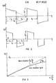
- the secondary supply alternating currents IS 'and IS cannot have an ideal rectangular shape. Rather, they show sloping ceilings in the form of e-functions how this in a
- T is a time constant which is determined by the values of the stray and main inductance of the current transformer Tr2, the internal resistance of the direct current source and the compensation resistance.
- the arithmetic mean U ⁇ m ⁇ from the sum Um of the output voltages Umy of all n transducers DMSy is always formed by the known compensator circuit over the full switching period T A , that is But with that With and where cy is a transducer sensitivity constant.
- the mean value Um is strictly linearly proportional to the sum of the measurement variables Gy acting on the n transducers DMSy at any moment, despite the roof slopes of the individual signals Umy embodied by ⁇ ⁇ .
- a duty ratio a t e / T
- a proportional indication value A of the known compensator is the matching condition won. Because of the sub-linearity of Uk, the known compensator circuit must therefore have an over-linear display characteristic as a whole.
- the object of the invention was to improve the evaluation circuit for passive measuring sensors described at the outset in such a way that it obtains a linear display characteristic.
- Their advantages with regard to insensitivity to thermal and contact voltages of the transducers, the compensation size generator and the input installation as well as to zero drift of the amplification should be retained.
- the first measure relates to the displacement of the zero amplifier NV provided in the known circuit according to FIG. 1 behind the low-pass filter TP using a directly coupled preamplifier at the previous location of the zero amplifier.
- This preamplifier expediently consists of an operational amplifier which is galvanically connected to an output of the network emitting the adjustment differential voltage or an adjustment differential current and comprises, if appropriate, associated coupling elements. It has a phase-linear frequency response beginning at frequency 0 (DC components permeable), which is broadband over the polarity reversal frequency amplified beyond. Its amplitude response need not be particularly flat. The amplification can fluctuate over long periods with respect to the cycle time T A without influencing the display accuracy.
- the preamplifier has only a relatively low gain to ensure that it is capacitive tive or inductive interference in the input wiring or through its own noise components and zero drifts in the balanced state of the evaluation device is not operated beyond its control limits.
- Another measure relates to the direct coupling of the current flowing through the switchable resistor to the pole changer of the direct current source. It ensures that this stream has a strictly rectangular shape and no sloping roof causing linearity errors.
- the adjustment difference signal is amplified in such a way that identical components which distort the correct display value can arise as zero-point errors neither due to runtime distortions nor due to nonlinear modulations in the subsequent phase-sensitive rectification.
- the phase-sensitive rectifier expediently has a strictly linear characteristic curve which runs exactly through the zero point.
- the noise components all experience a frequency shift of + fW during the demodulation process Inverter frequency f W.
- the very disturbing low-frequency noise components of simple semiconductor amplifier input stages the so-called popcorn or noise, are shifted into the immediate vicinity of the inverter frequency f W and can also be effectively suppressed by the subsequent low-pass filters. Therefore, only the so-called white noise represents the natural resolution limit of the evaluation circuit according to the invention.
- the synchronous control of the phase-sensitive rectifier with the pole-changing switch ensures that a higher accuracy requirements sufficient suppression of the mentioned disturbing DC components in the amplified adjustment difference signal is achieved because it also controls the selective rectifier in strict time symmetry.
- the generator for the high-frequency pulse train is appropriately quartz-stabilized.
- the symmetry of two branches of the phase-sensitive rectifier with respect to ground is advantageously made adjustable by a potentiometer.
- the transducer bridge circuits are also advantageously galvanically coupled to the pole switch.
- transducer bridge circuit and / or the switchable resistor are coupled to the pole switch via operational amplifiers or optocouplers.
- the direct coupling of a transducer bridge circuit and a switchable resistor is realized in that the bridge circuit with its supply diagonal is galvanically coupled to the pole switch and is separated at one of its diagonal points.
- the switchable resistor is inserted into the disconnection point, the changeover contact arm of the switch replacing the diagonal point at the disconnection point.
- the input terminals of the preamplifier are on the diagonal of the transducer bridge circuit.
- the supply diagonal of the transducer bridge circuit is galvanically coupled to the pole switch.
- the switchable resistor is connected between the output of a first operational amplifier with its input terminals on the pole-changing switch and ground.
- the measuring diagonal of the transducer bridge circuit is connected to the input terminals of a second operational amplifier, the output of which is connected to ground via a resistor and to an input terminal of the preamplifier.
- the preamplifier is connected with its other input terminal to the changeover contact arm of the changeover switch, which is in one position at the output of the first operational amplifier and in the other position to ground.
- the feed diagonal of the transducer bridge circuit is galvanically coupled to the pole switch.
- the switchable resistor is connected via the switch between the output of a first operational amplifier with its input terminals on the pole switch and ground.
- the measuring diagonal of the transducer bridge circuit is connected to the input terminals of a second operational amplifier, the output of which is connected via a resistor to that input terminal of the preamplifier which is connected to one of the changeover contacts of the changeover switch.
- the other input terminal of the preamplifier is grounded.
- the direct coupling feature is realized in another embodiment of the invention so that a second resistance bridge circuit is connected in parallel on the supply and measurement diagonal side of the transducer bridge circuit, the second resistance bridge circuit being separated at a measurement diagonal point and the switchable resistor being inserted into the separation point.
- the input terminals of the preamplifier are connected to the parallel measuring diagonals of the two resistor bridge circuits.
- a half-bridge circuit can also be used, the branches of which include the switchable resistor.
- Yet another exemplary embodiment of the invention has a second resistor bridge connected in parallel on the supply and measurement diagonal side of the transducer bridge circuit, which is separated at a feed diagonal point, the separation point being occupied by two contacts of the changeover switch.
- the changeover contact arm of the changeover switch is located at one of the feed diagonal points of the transducer bridge circuit.
- the input terminals of the preamplifier are connected to the parallel measuring diagonals of the two resistor bridge circuits.
- a last exemplary embodiment of the invention has a changeover resistor which, with the aid of the changeover switch, can be connected in parallel to two resistors of the transducer bridge circuit which are symmetrical about a diagonal point, the input terminals of the preamplifier being located on the measurement diagonal.
- the duration of an adjustment period T A is related to the duration T W of the inverter and rectifier cycle time in the ratio of integers (e.g. 1: 2; 2: 3; 3: 5 etc.).
- FIG. 4 contains an exemplary embodiment of the invention in which detuning compensation is used.
- FIG. 5 shows in diagrams a, b and c the voltage curves occurring at characteristic switching points of the circuit according to FIG.
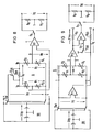
- FIG. 6 shows a modified detail of the circuit according to FIG. 4.
- FIGS. 7 to 13 each show different versions of the direct coupling of the transducer and compensation network to the inverter or pole-reversal switch.
- a preferably earth-symmetrical voltage source SQ is connected via switching paths T P1 ... T P4 , which form a pole-changing switch or inverter SW, to a measured variable pickup G, which is shown as a pickup measuring bridge with four variable resistors R 1 ... R 4 .
- a balancing resistor R K is alternately connected in parallel to the measuring bridge resistors R 1 and R 2 via switching paths T 01 and T 02 .
- the switching paths T P1 ... T P4 of the pole changer or inverter are controlled by output signals from a flip-flop FF 1 .
- a dynamic input of the flip-flop FF 1 is at an output for an overflow signal ü from a counter Z, which is acted upon by clock pulses from a clock generator TG.
- Bit outputs of the clock pulse counter Z are connected to corresponding inputs of a digital comparator V, the comparison bit inputs of which are connected to bit outputs of a display counter A.
- a digital comparator V which is signal-carrying is one with one of the control inputs second flip-flops FF 2 connected.
- the other control input of the flip-flop FF 2 is connected to the output of the counter Z, which outputs the overflow signal ü z .
- the two outputs of the flip-flop FF 2 are each connected to a control input of one of the switching paths T 01 or T 02 .
- the measuring diagonal of the transducer G is at the inputs of a preamplifier VV.
- the output of this preamplifier VV is connected to the input of a phase-sensitive rectifier D, which essentially consists of the switching paths T G1 and T G2 .
- Control inputs of the switching paths T G1 and T G2 are connected to two mutually inverted signals leading outputs of the flip-flop FF 1 , which simultaneously control the switching paths of the pole changer or inverter SW.
- the two branches of the phase-sensitive rectifier D can be centered via a potentiometer PL connecting the two branches.
- the output of the phase-sensitive rectifier D is connected via a first low-pass element T 1 to the inputs of a post-amplifier NV acting as a DC voltage zero amplifier, the output of which is connected via a second low-pass element T 2 to the input of a voltage-frequency converter UF.
- a post-amplifier NV acting as a DC voltage zero amplifier
- T 2 the input of a voltage-frequency converter UF.
- one of two outputs of the voltage-frequency converter becomes the signal leader.
- the two outputs are connected to corresponding inputs for up and down counting of the display counter A.
- Bit outputs of the display counter A are connected to the corresponding inputs of a digital display ZA.
- T A is the time required to count the clock pulse counter Z up to its maximum value Z max by the pulses with the repetitive frequency f t supplied by the short-term stable clock generator TG.
- the overflow pulse ü z supplied by the counter Z after it has been fully counted once sets the clock pulse counter Z itself to "0" and at the same time acts on the dynamic input of the flip-flop FF 1 , which thereby results after the time T A has elapsed Switching state changes.
- the switching paths Tp2 and T P4 of the inverter SW or pole changer are alternately controlled for passage for an n-th cycle time T An to the switching distances T P1 and T P3 and for the subsequent cycle time T An + 1 , so that at the diagonal of the transducer G a square wave voltage U S with the required exact clock ratio 1: 1 is available. Phase-locked and strictly synchronous with the switching paths T P1 ...
- the switching paths T G1 and T G2 of the phase-sensitive rectifier D are also controlled for transmission from the respective position of the flip-flop FF 1 alternately for the duration of the time T A .
- the phase-sensitive rectifier D demodulates the output voltage of the preamplifier VV.
- the preamplifier VV is DC-coupled to the measurement diagonal of the transducer G and works as a phase-linear broadband amplifier with a highly linear control characteristic from a frequency of 0. It therefore amplifies the transducer measurement voltage u, which, in addition to the unwanted interference components consisting of thermal voltages and contact potentials, exclusively includes alternating components has whose fundamental frequency is and otherwise consists of their harmonics.
- the preamplifier VV continues to amplify undesired DC components which result from the current and voltage zero drifts of the preamplifier VV itself. The effect of these zero drifts is combined with the thermal and contact voltages of the transducer and compensation network in an equivalent voltage u O.
- the preamplifier VV also amplifies all noise voltage components that are mainly generated in the input stage of the preamplifier VV, but also as white resistance noise in the pickup and compensation network.
- Another result of the operation of the new circuit is also advantageous, which consists in the fact that the noise components of the output signal of the preamplifier VV all experience a frequency shift of + f W during the demodulation process.
- the noise components of the so-called white noise which are smaller by orders of magnitude, are not suppressed.
- the measuring voltage components originating in the um have a rectangular voltage profile with an amplitude of which is due to the construction of the transducer and compensation network from purely ohmic resistors exactly in phase with U S
- the factor b therefore indicates the degree of partial modulation of this measuring range. It can therefore take values between 0 and 1.
- the square-wave voltage b ⁇ û m is converted by the phase-sensitive rectifier D with the correct sign into a proportional DC voltage, which can pass the low-pass filter T 1 and, after amplification by the post-amplifier NV, can also pass through the low-pass filter T 2 without undue sign and in the subsequent voltage evaluation
- Frequency converter UF is converted into a pulse train z Iauf or z Iab with a repetition frequency proportional to the respective residual detuning of the transducer.
- the counter pulses Z Iauf and Z Iab generated in this way serve to display the current counter content of the display counter A with its - four in the exemplary embodiment - To change counting decades AT A H , A Z and A E in the sense of an approximation to the trimming state of the measuring circuit given by b in the upward or downward direction.
- the preamplifier VV has a modulation characteristic which is strictly linear, at least in the frequency range f w - f d y n max to f w + f dynmax,
- the phase-sensitive rectifier D operates strictly symmetrically and also with a highly linear characteristic. It is therefore expedient to prepare a possibility for fine adjustment of this symmetry in the phase-sensitive rectifier D with the aid of a trim potentiometer PL.
- the sensor supply voltage U S is set to "0" for a short period of time t ü1 by a correspondingly designed control system after the occurrence of an overflow signal ü z by blocking the last conductive inverter switching paths T P1 , T P3 or T P2 , T P4 .
- the resistance R K is switched by the switching path T 01 or T 02 and the phase-sensitive rectifier D is reversed after t t1 .
- FIG. 5 shows the course of the supply voltage U S of the measuring sensor along the time axis t.
- the amplitude of the rectangular AC voltage, which is generated by polarity reversal, is 2 U B.
- the period of the AC voltage is 2 T A.
- the half period T A is the product of the maximum content Z max of the counter Z divided by the repetition frequency f t of the counting pulses entering the counter Z.
- the output voltage u a of the phase-sensitive rectifier D can also be changed by them Alternating components of u m no longer result in a constant component 0 which could pass through the low-pass filters T 1 and T 2 and which would thereby incorrectly influence the adjustment value of the evaluation circuit. However, this would very well happen if the phase-sensitive rectifier were reversed at times that do not exactly coincide with t start . This is where the demand for an extremely time-exact control of the demodulator D assigned to the polarity reverser of the supply voltage arises.
- the demodulated signal in the trimmed state has no DC components which influence the trimming value, since the demodulator chops the amplified DC spurious voltages into square-wave AC voltages of the fundamental frequency f w .
- a prerequisite for this is that the demodulator D has a strictly linear characteristic that goes exactly through 0.
- FIG. 6 shows a further exemplary embodiment for a directly coupled measurement variable pickup G and a compensation resistor R K6 , in which detuning compensation is used.
- a pole-reversal switch SW is connected to a supply voltage source SQ with the voltage 2 U B and supplies the supply diagonal of a measured variable pickup G with a square-wave voltage U s .
- the measured variable pickup G consists of a bridge circuit of four resistors R1 ... R 4 variable with one measured variable. The connection points of this bridge circuit are named 1 ... 4.
- a compensation resistor RK6 with which detuning compensation of the output signal of the measured variable pickup G can be carried out, is not permanently connected to a corner point of the output diagonals, but to a feed diagonal point.
- the compensation resistor R K6 can be connected alternately to both diagonal points 2, 3 of the output diagonals and thus one of the bridge resistors R 1 or R 3 can be connected in parallel.
- This switchover makes the adjustment factor Tor a controlled so that the measurement-related detuning the measured value pickup bridge G is just made to 0 on average over time by counter-detuning the bridge.
- the instantaneous size of the detuning is determined by means of the open-circuit measurement voltage, which arises at the output diagonal of the measurement variable pickup G and is amplified in the preamplifier VV.
- the transducer G again consists of four resistors R 1 ... R 4 interconnected to form a Wheatstone bridge circuit, the supply diagonal points 1 and 4 of which are connected to a supply voltage U S , which can be switched via the periodically switchable switch SW at the supply source SQ with the direct voltage 2 U B lie.
- the bridge is separated and a compensation resistor R K7 is inserted into the separation points 3a, 3b.
- the transducer G is shown here as a full-bridge circuit, but it goes without saying that a quarter or half-bridge circuit can also be used.
- the bridge points 3a and a changeover switch S 3b U7 to the one input of the preamplifier can VV are placed alternately with the aid, the other input to the output 2 of the diagonal point Me ß wholesomenauf choirs G is connected.
- the rest of the circuit, not shown, for evaluating the output voltage of the phase-sensitive rectifier D and for controlling the changeover switch corresponds to the details which can be seen in FIG.
- FIG. 7 A circuit which largely corresponds to the circuit according to FIG. 7 is shown in FIG. It differs from the circuit according to FIG. 7 in that the feed diagonal point 1 of the measured variable pickup bridge G is separated and a compensation resistor R K8 is inserted at the separation point 1a, 1b.
- a changeover switch S U8 alternately applies one of the points 1a and 1b to the output voltage U s of the changeover switch SW. Voltage compensation is also present in the circuit according to FIG. 8.
- FIG. 9 shows a further transducer compensation and rectifier complex which works on the principle of voltage compensation.
- the voltage is amplified by an output amplifier V T2 at the output diagonal of the transducer G.
- a compensation resistor R K9 is connected to the output voltage U s of the pole-reversal switch SW via another operational amplifier VT1 .
- One of the input terminals of the preamplifier VV is at the output of the operational amplifier VT2, the other input terminal is alternately acted upon by a change-over switch S U9 with the voltage drop ü K at the compensation resistor R K9 and ground potential.
- the input voltage of the preamplifier VV is shown where v is the gain of the operational amplifier VT2.
- FIG. 10 shows an example of a circuit for a transducer and compensation network that works on the principle of current compensation.
- a transducer bridge circuit G and a compensation bridge circuit K which consists of four resistors R 1 '... R 4 ' and a switchable resistor R K10 , are connected in parallel with their supply diagonals and output diagonals. On the supply side, both are connected to the pole-reversal switch SW and thus to its output voltage U S.
- One of the output diagonal points of the compensation bridge K is separated, between the separation points is the switchable resistor R K10 ', the two connection points of which are alternately connected by a switch S U10 to the one input of the preamplifier VV.
- the other input of the preamplifier VV is connected to two interconnected output diagonal points of the two bridge circuits G and K.
- a short-circuit current is compensated from the diagonals of the transducer bridge G against the short-circuit current i k of the compensation bridge circuit K.
- all bridge resistors of the compensation bridge circuit K are designed to be high-impedance.
- FIG. 11 A variant of the circuit according to FIG. 10 is shown in FIG. 11.
- the bridge circuit K is closed a half bridge of the resistors R 3 'and R 4 ' with the interposed switchable resistor R K11 has been reduced.
- This variant can be easily obtained if the resistances R 1 'and R 2 ' of the circuit according to FIG. 10 are made infinitely large.
- FIG. 1 A further exemplary embodiment, in which current compensation is used with a compensation bridge circuit, is shown schematically in FIG. Only the compensation bridge K from the resistors R 1 '... R 4 ' and its connection to the bridge branch of the transducer bridge G consisting of the resistors R 3 and R 4 are shown.
- FIG. 13 shows an example of current compensation for the transducer output signal.
- the output diagonal points 2 and 3 of the transducer bridge circuit G are at the two inputs of an operational amplifier VT4, the output of which is connected via a resistor to one input of the preamplifier VV.
- the periodically switched supply voltage U s is connected to the inputs of a further operational amplifier V T3 , the output of which can be connected alternately to ground and the input of the preamplifier VV via a resistor and a changeover switch S U13 .
- the other input of the preamplifier VV is grounded.
- the illustrated exemplary embodiments all have the feature of the direct voltage-permeable coupling of the measurement variable pickup and compensation network to the pole changing switch SW.
- the options for designing the compensation shown do not claim to be complete. It is possible from the ones described here NEN basic solutions to derive mixed circuit arrangements in which the measures on which the invention is based are also applied.
Landscapes
- Physics & Mathematics (AREA)
- General Physics & Mathematics (AREA)
- Measurement Of Resistance Or Impedance (AREA)
- Measuring Instrument Details And Bridges, And Automatic Balancing Devices (AREA)
- Burglar Alarm Systems (AREA)
- Indication And Recording Devices For Special Purposes And Tariff Metering Devices (AREA)
- Measuring Magnetic Variables (AREA)
- Investigating Or Analyzing Materials By The Use Of Electric Means (AREA)
Priority Applications (1)
| Application Number | Priority Date | Filing Date | Title |
|---|---|---|---|
| AT84109449T ATE26490T1 (de) | 1983-08-26 | 1984-08-08 | Auswerteschaltungen fuer passive messgroessenaufnehmer. |
Applications Claiming Priority (2)
| Application Number | Priority Date | Filing Date | Title |
|---|---|---|---|
| DE3330841 | 1983-08-26 | ||
| DE3330841A DE3330841A1 (de) | 1983-08-26 | 1983-08-26 | Auswerteschaltungen fuer passive messgroessenaufnehmer |
Publications (2)
| Publication Number | Publication Date |
|---|---|
| EP0141080A1 true EP0141080A1 (fr) | 1985-05-15 |
| EP0141080B1 EP0141080B1 (fr) | 1987-04-08 |
Family
ID=6207523
Family Applications (1)
| Application Number | Title | Priority Date | Filing Date |
|---|---|---|---|
| EP84109449A Expired EP0141080B1 (fr) | 1983-08-26 | 1984-08-08 | Circuits d'évaluation pour des capteurs de mesure passifs |
Country Status (6)
| Country | Link |
|---|---|
| US (1) | US4618818A (fr) |
| EP (1) | EP0141080B1 (fr) |
| JP (1) | JPS60220875A (fr) |
| AT (1) | ATE26490T1 (fr) |
| DE (2) | DE3330841A1 (fr) |
| ES (1) | ES8505102A1 (fr) |
Cited By (5)
| Publication number | Priority date | Publication date | Assignee | Title |
|---|---|---|---|---|
| EP0196912A1 (fr) * | 1985-03-29 | 1986-10-08 | Honeywell Inc. | Pont de mesure capacitif |
| EP0250028A3 (en) * | 1986-06-18 | 1989-05-31 | Philips Patentverwaltung Gmbh | Circuit device for compensation of temperature dependent and temperature independent drifts of a capacitive sensor |
| EP0366831A1 (fr) * | 1988-11-04 | 1990-05-09 | Horiba, Ltd. | Circuit compensateur de température |
| FR2670901A1 (fr) * | 1990-11-26 | 1992-06-26 | Precia Sa | Dispositif d'amplification du signal de desequilibre d'un pont de wheatstone, destine a etre incorpore notamment a une balance de haute precision. |
| DE19509815C1 (de) * | 1995-03-22 | 1996-10-31 | Joachim Dr Scheerer | Schaltung zur Speisung einer Wheatstoneschen Brücke mit einer Rechteckwechselspannung |
Families Citing this family (17)
| Publication number | Priority date | Publication date | Assignee | Title |
|---|---|---|---|---|
| US4786875A (en) * | 1986-07-22 | 1988-11-22 | General Signal Corporation | Conductivity measuring circuit |
| DE3633790A1 (de) * | 1986-10-03 | 1988-04-14 | Endress Hauser Gmbh Co | Anordnung zur aufbereitung der ausgangssignale einer widerstandsbruecke |
| DE3710904A1 (de) * | 1987-04-01 | 1988-10-13 | Siemens Ag | Verfahren und anordnung zur auswertung einer analogen elektrischen messgroesse |
| DE4417228A1 (de) † | 1994-05-17 | 1995-11-23 | Michael Dr Altwein | Dehnungsmeßstreifen-Meßanordnung, Verwendung derselben und Modulationsverstärker für derartige Meßanordnungen |
| CA2150502A1 (fr) * | 1994-08-05 | 1996-02-06 | Michael F. Mattes | Methode et appareil servant a mesurer la temperature |
| US5764067A (en) * | 1995-05-10 | 1998-06-09 | Rastegar; Ali J. | Method and apparatus for sensor signal conditioning using low-cost, high-accuracy analog circuitry |
| US6268818B1 (en) * | 1998-06-24 | 2001-07-31 | Conexant Systems, Inc. | Method and apparatus for improving modulation accuracy |
| US6198296B1 (en) | 1999-01-14 | 2001-03-06 | Burr-Brown Corporation | Bridge sensor linearization circuit and method |
| SE513954C2 (sv) * | 1999-04-01 | 2000-12-04 | Abb Ab | Förfarande och system för bearbetning av signaler från en givare driven med en växelströmsexcitationssignal |
| JP3588276B2 (ja) | 1999-07-26 | 2004-11-10 | 株式会社山武 | センサ信号処理回路 |
| DE10216344A1 (de) * | 2002-04-13 | 2003-10-23 | Hottinger Messtechnik Baldwin | Meßverstärkervorrichtung |
| JP2005300495A (ja) * | 2004-04-16 | 2005-10-27 | Agilent Technol Inc | 半導体特性測定装置および接続装置 |
| US20140015551A1 (en) * | 2010-03-17 | 2014-01-16 | Samuel H. Russ | Salinity sensor for embedded environmental monitoring |
| DE102011104307B4 (de) * | 2011-06-16 | 2013-09-26 | Austriamicrosystems Ag | Anordnung und Verfahren zum Betreiben eines Sensors, insbesondere eines Brückensensors, und eine Sensoranordnung |
| JP6510199B2 (ja) * | 2014-08-19 | 2019-05-08 | ローム株式会社 | スイッチング回路、オーディオアンプ集積回路、電子機器、電気音響変換素子の駆動方法 |
| US20220149856A1 (en) * | 2020-11-11 | 2022-05-12 | Microsoft Technology Licensing, Llc | Bridge sensor dc error cancellation scheme |
| US11588493B2 (en) * | 2021-05-28 | 2023-02-21 | Taiwan Semiconductor Manufacturing Company Ltd. | Circuitry and method for reducing environmental noise |
Citations (2)
| Publication number | Priority date | Publication date | Assignee | Title |
|---|---|---|---|---|
| DE2260441A1 (de) * | 1972-12-11 | 1974-06-27 | Siemens Ag | Analog-digital-wandler |
| DE2841830B1 (de) * | 1978-09-26 | 1980-01-24 | Siemens Ag | Schaltungsanordnung zur Messung der Messdiagonalspannung einer Widerstandsbrueckenschaltung |
Family Cites Families (5)
| Publication number | Priority date | Publication date | Assignee | Title |
|---|---|---|---|---|
| US3588690A (en) * | 1969-07-16 | 1971-06-28 | Hugh Allen Griffin | Test circuit including bridge type oscillator means for monitoring equivalent series resistance of quartz crystals |
| JPS5650232B2 (fr) * | 1972-11-15 | 1981-11-27 | ||
| DE2262755C3 (de) * | 1972-12-21 | 1975-08-07 | Siemens Ag, 1000 Berlin Und 8000 Muenchen | Digitale Kompensationseinrichtung |
| US3944819A (en) * | 1975-02-26 | 1976-03-16 | Amf Incorporated | Produce grader |
| JPS55112014A (en) * | 1979-02-21 | 1980-08-29 | Masaoki Ishikawa | Chopper amplifier |
-
1983
- 1983-08-26 DE DE3330841A patent/DE3330841A1/de not_active Withdrawn
-
1984
- 1984-08-08 DE DE8484109449T patent/DE3463089D1/de not_active Expired
- 1984-08-08 EP EP84109449A patent/EP0141080B1/fr not_active Expired
- 1984-08-08 AT AT84109449T patent/ATE26490T1/de not_active IP Right Cessation
- 1984-08-24 JP JP59176514A patent/JPS60220875A/ja active Pending
- 1984-08-24 US US06/643,875 patent/US4618818A/en not_active Expired - Fee Related
- 1984-08-24 ES ES535406A patent/ES8505102A1/es not_active Expired
Patent Citations (2)
| Publication number | Priority date | Publication date | Assignee | Title |
|---|---|---|---|---|
| DE2260441A1 (de) * | 1972-12-11 | 1974-06-27 | Siemens Ag | Analog-digital-wandler |
| DE2841830B1 (de) * | 1978-09-26 | 1980-01-24 | Siemens Ag | Schaltungsanordnung zur Messung der Messdiagonalspannung einer Widerstandsbrueckenschaltung |
Non-Patent Citations (2)
| Title |
|---|
| ELECTRONIC DESIGN, Band 29, Nr. 16, August 1981, Seiten 203-206, Waseca, MN, USA; J. WILLIAMS: "IC instrumentation amp enhances transducer measurements" * |
| PROCEEDINGS IEE, Band 119, Nr. 1, Januar 1972, Seiten 108-112; S. SUZUKI: "Square-wave-source gated-detector bridge system for the precise measurement of resistance" * |
Cited By (5)
| Publication number | Priority date | Publication date | Assignee | Title |
|---|---|---|---|---|
| EP0196912A1 (fr) * | 1985-03-29 | 1986-10-08 | Honeywell Inc. | Pont de mesure capacitif |
| EP0250028A3 (en) * | 1986-06-18 | 1989-05-31 | Philips Patentverwaltung Gmbh | Circuit device for compensation of temperature dependent and temperature independent drifts of a capacitive sensor |
| EP0366831A1 (fr) * | 1988-11-04 | 1990-05-09 | Horiba, Ltd. | Circuit compensateur de température |
| FR2670901A1 (fr) * | 1990-11-26 | 1992-06-26 | Precia Sa | Dispositif d'amplification du signal de desequilibre d'un pont de wheatstone, destine a etre incorpore notamment a une balance de haute precision. |
| DE19509815C1 (de) * | 1995-03-22 | 1996-10-31 | Joachim Dr Scheerer | Schaltung zur Speisung einer Wheatstoneschen Brücke mit einer Rechteckwechselspannung |
Also Published As
| Publication number | Publication date |
|---|---|
| DE3330841A1 (de) | 1985-03-14 |
| EP0141080B1 (fr) | 1987-04-08 |
| JPS60220875A (ja) | 1985-11-05 |
| ES535406A0 (es) | 1985-05-01 |
| US4618818A (en) | 1986-10-21 |
| ES8505102A1 (es) | 1985-05-01 |
| DE3463089D1 (en) | 1987-05-14 |
| ATE26490T1 (de) | 1987-04-15 |
Similar Documents
| Publication | Publication Date | Title |
|---|---|---|
| EP0141080B1 (fr) | Circuits d'évaluation pour des capteurs de mesure passifs | |
| DE10223767B4 (de) | Schaltungsanordnung zum Verarbeiten eines Signals eines Sensors | |
| EP0521448A2 (fr) | Circuit pour la détermination des erreurs d'un débitmètre magnétique-inductif | |
| DE102018201310B4 (de) | Stromsensor und Schutzschalter | |
| WO2012098054A1 (fr) | Dispositif de mesure de courant | |
| DE19844663C2 (de) | Schaltungsanordnung und Verfahren zum Einstellen von Schaltpunkten eines Entscheiders | |
| DE2906492C2 (de) | Signalverarbeitungsschaltung für ein Tonfrequenzsignal und ein Abstimmanzeige-Steuersignal | |
| DE102021104752B4 (de) | Stromsensor für die berührungslose strommessung | |
| EP0025029B1 (fr) | Dispositif de pont de mesure capacitif | |
| DE29714612U1 (de) | Strom-Meßeinrichtung | |
| DE10216344A1 (de) | Meßverstärkervorrichtung | |
| EP0250028B1 (fr) | Dispositif de montage pour la compensation de dérivés dépendants ou non de la température d'un capteur capacitif | |
| DE2222795C3 (de) | Filter für ein amplitudenmoduliertes Trägerfrequenzmeßsystem | |
| DE102004056384A1 (de) | Verfahren zur Offseteliminierung aus Signalen magnetoresistiver Sensoren | |
| EP0412573B1 (fr) | Circuit de conversion d'un signal analogique en fréquence | |
| EP1091214B1 (fr) | Procédé et dispositif de traitement de signaux de mesure | |
| DE3143669C2 (de) | Schaltung zum Messen des Effektivwertes einer Wechselspannung | |
| EP0137896B1 (fr) | Circuit pour compenser les variations du facteur de transfert d'une sonde linéaire de champ magnétique | |
| DE4427547C2 (de) | Induktiver Fahrzeug-Detektor | |
| DE1773847C3 (de) | Schaltungsanordnung zur Filterung eines im Audio-Frequenzbereich Hegenden Ausgangssignals | |
| DE1466741C3 (de) | Schaltungsanordnung zur Messung des Amplitudenverhältnisses zweier elektrischer Wechselgrößen | |
| DE1437943C (de) | Verstärker | |
| DE3611682C2 (de) | Meßanordnung mit einem aktiven Filter | |
| DE19844729A1 (de) | Stromsensor | |
| DE3616711A1 (de) | Signalumformer |
Legal Events
| Date | Code | Title | Description |
|---|---|---|---|
| PUAI | Public reference made under article 153(3) epc to a published international application that has entered the european phase |
Free format text: ORIGINAL CODE: 0009012 |
|
| AK | Designated contracting states |
Designated state(s): AT BE CH DE FR GB IT LI LU NL SE |
|
| 17P | Request for examination filed |
Effective date: 19850604 |
|
| 17Q | First examination report despatched |
Effective date: 19860527 |
|
| GRAA | (expected) grant |
Free format text: ORIGINAL CODE: 0009210 |
|
| AK | Designated contracting states |
Kind code of ref document: B1 Designated state(s): AT BE CH DE FR GB IT LI LU NL SE |
|
| REF | Corresponds to: |
Ref document number: 26490 Country of ref document: AT Date of ref document: 19870415 Kind code of ref document: T |
|
| REF | Corresponds to: |
Ref document number: 3463089 Country of ref document: DE Date of ref document: 19870514 |
|
| ET | Fr: translation filed | ||
| ITF | It: translation for a ep patent filed | ||
| PG25 | Lapsed in a contracting state [announced via postgrant information from national office to epo] |
Ref country code: LU Free format text: LAPSE BECAUSE OF NON-PAYMENT OF DUE FEES Effective date: 19870831 |
|
| PLBE | No opposition filed within time limit |
Free format text: ORIGINAL CODE: 0009261 |
|
| STAA | Information on the status of an ep patent application or granted ep patent |
Free format text: STATUS: NO OPPOSITION FILED WITHIN TIME LIMIT |
|
| 26N | No opposition filed | ||
| PGFP | Annual fee paid to national office [announced via postgrant information from national office to epo] |
Ref country code: AT Payment date: 19890803 Year of fee payment: 6 |
|
| PGFP | Annual fee paid to national office [announced via postgrant information from national office to epo] |
Ref country code: LU Payment date: 19890811 Year of fee payment: 6 |
|
| PGFP | Annual fee paid to national office [announced via postgrant information from national office to epo] |
Ref country code: BE Payment date: 19890824 Year of fee payment: 6 |
|
| ITTA | It: last paid annual fee | ||
| PG25 | Lapsed in a contracting state [announced via postgrant information from national office to epo] |
Ref country code: AT Effective date: 19900808 |
|
| PG25 | Lapsed in a contracting state [announced via postgrant information from national office to epo] |
Ref country code: BE Effective date: 19900831 |
|
| BERE | Be: lapsed |
Owner name: SIEMENS A.G. BERLIN UND MUNCHEN Effective date: 19900831 |
|
| PGFP | Annual fee paid to national office [announced via postgrant information from national office to epo] |
Ref country code: GB Payment date: 19910718 Year of fee payment: 8 |
|
| PGFP | Annual fee paid to national office [announced via postgrant information from national office to epo] |
Ref country code: SE Payment date: 19910816 Year of fee payment: 8 |
|
| PGFP | Annual fee paid to national office [announced via postgrant information from national office to epo] |
Ref country code: FR Payment date: 19910823 Year of fee payment: 8 |
|
| PGFP | Annual fee paid to national office [announced via postgrant information from national office to epo] |
Ref country code: NL Payment date: 19910831 Year of fee payment: 8 |
|
| PGFP | Annual fee paid to national office [announced via postgrant information from national office to epo] |
Ref country code: DE Payment date: 19911029 Year of fee payment: 8 |
|
| PGFP | Annual fee paid to national office [announced via postgrant information from national office to epo] |
Ref country code: CH Payment date: 19911122 Year of fee payment: 8 |
|
| PG25 | Lapsed in a contracting state [announced via postgrant information from national office to epo] |
Ref country code: GB Effective date: 19920808 |
|
| PG25 | Lapsed in a contracting state [announced via postgrant information from national office to epo] |
Ref country code: SE Effective date: 19920809 |
|
| PG25 | Lapsed in a contracting state [announced via postgrant information from national office to epo] |
Ref country code: LI Effective date: 19920831 Ref country code: CH Effective date: 19920831 |
|
| PG25 | Lapsed in a contracting state [announced via postgrant information from national office to epo] |
Ref country code: NL Effective date: 19930301 |
|
| GBPC | Gb: european patent ceased through non-payment of renewal fee |
Effective date: 19920808 |
|
| NLV4 | Nl: lapsed or anulled due to non-payment of the annual fee | ||
| PG25 | Lapsed in a contracting state [announced via postgrant information from national office to epo] |
Ref country code: FR Effective date: 19930430 |
|
| REG | Reference to a national code |
Ref country code: CH Ref legal event code: PL |
|
| PG25 | Lapsed in a contracting state [announced via postgrant information from national office to epo] |
Ref country code: DE Effective date: 19930501 |
|
| REG | Reference to a national code |
Ref country code: FR Ref legal event code: ST |
|
| EUG | Se: european patent has lapsed |
Ref document number: 84109449.3 Effective date: 19930307 |