EP0141114A1 - Vorrichtung zum kontinuierlichen Niederschlagen einer Schicht aus polykristallinem Silizium auf einem Kohlenstoffband - Google Patents
Vorrichtung zum kontinuierlichen Niederschlagen einer Schicht aus polykristallinem Silizium auf einem Kohlenstoffband Download PDFInfo
- Publication number
- EP0141114A1 EP0141114A1 EP84110062A EP84110062A EP0141114A1 EP 0141114 A1 EP0141114 A1 EP 0141114A1 EP 84110062 A EP84110062 A EP 84110062A EP 84110062 A EP84110062 A EP 84110062A EP 0141114 A1 EP0141114 A1 EP 0141114A1
- Authority
- EP
- European Patent Office
- Prior art keywords
- silicon
- crucible
- bath
- image
- output
- Prior art date
- Legal status (The legal status is an assumption and is not a legal conclusion. Google has not performed a legal analysis and makes no representation as to the accuracy of the status listed.)
- Granted
Links
- OKTJSMMVPCPJKN-UHFFFAOYSA-N Carbon Chemical compound [C] OKTJSMMVPCPJKN-UHFFFAOYSA-N 0.000 title claims abstract description 17
- 229910052799 carbon Inorganic materials 0.000 title claims abstract description 17
- 229910021420 polycrystalline silicon Inorganic materials 0.000 title claims description 10
- 230000008021 deposition Effects 0.000 title description 3
- 229910052710 silicon Inorganic materials 0.000 claims abstract description 67
- 239000010703 silicon Substances 0.000 claims abstract description 67
- 230000003287 optical effect Effects 0.000 claims abstract description 15
- 239000007788 liquid Substances 0.000 claims abstract description 11
- 239000007787 solid Substances 0.000 claims abstract description 11
- XUIMIQQOPSSXEZ-UHFFFAOYSA-N Silicon Chemical compound [Si] XUIMIQQOPSSXEZ-UHFFFAOYSA-N 0.000 claims description 69
- 238000005259 measurement Methods 0.000 claims description 10
- 238000000926 separation method Methods 0.000 claims description 7
- 238000010438 heat treatment Methods 0.000 claims description 6
- 238000000151 deposition Methods 0.000 claims description 5
- 238000004519 manufacturing process Methods 0.000 abstract description 3
- 239000000523 sample Substances 0.000 description 5
- VYPSYNLAJGMNEJ-UHFFFAOYSA-N Silicium dioxide Chemical compound O=[Si]=O VYPSYNLAJGMNEJ-UHFFFAOYSA-N 0.000 description 4
- 239000000463 material Substances 0.000 description 4
- YFXPPSKYMBTNAV-UHFFFAOYSA-N bensultap Chemical compound C=1C=CC=CC=1S(=O)(=O)SCC(N(C)C)CSS(=O)(=O)C1=CC=CC=C1 YFXPPSKYMBTNAV-UHFFFAOYSA-N 0.000 description 3
- 238000010586 diagram Methods 0.000 description 3
- 239000008188 pellet Substances 0.000 description 3
- 235000012431 wafers Nutrition 0.000 description 3
- 230000033228 biological regulation Effects 0.000 description 2
- 230000005251 gamma ray Effects 0.000 description 2
- 238000005286 illumination Methods 0.000 description 2
- 230000006698 induction Effects 0.000 description 2
- 230000008018 melting Effects 0.000 description 2
- 238000002844 melting Methods 0.000 description 2
- 230000005499 meniscus Effects 0.000 description 2
- 230000005855 radiation Effects 0.000 description 2
- 239000000377 silicon dioxide Substances 0.000 description 2
- 230000007423 decrease Effects 0.000 description 1
- 230000004907 flux Effects 0.000 description 1
- 238000011084 recovery Methods 0.000 description 1
- 230000035945 sensitivity Effects 0.000 description 1
Images


Classifications
-
- H—ELECTRICITY
- H10—SEMICONDUCTOR DEVICES; ELECTRIC SOLID-STATE DEVICES NOT OTHERWISE PROVIDED FOR
- H10F—INORGANIC SEMICONDUCTOR DEVICES SENSITIVE TO INFRARED RADIATION, LIGHT, ELECTROMAGNETIC RADIATION OF SHORTER WAVELENGTH OR CORPUSCULAR RADIATION
- H10F71/00—Manufacture or treatment of devices covered by this subclass
- H10F71/121—The active layers comprising only Group IV materials
- H10F71/1221—The active layers comprising only Group IV materials comprising polycrystalline silicon
-
- B—PERFORMING OPERATIONS; TRANSPORTING
- B05—SPRAYING OR ATOMISING IN GENERAL; APPLYING FLUENT MATERIALS TO SURFACES, IN GENERAL
- B05C—APPARATUS FOR APPLYING FLUENT MATERIALS TO SURFACES, IN GENERAL
- B05C3/00—Apparatus in which the work is brought into contact with a bulk quantity of liquid or other fluent material
- B05C3/02—Apparatus in which the work is brought into contact with a bulk quantity of liquid or other fluent material the work being immersed in the liquid or other fluent material
- B05C3/12—Apparatus in which the work is brought into contact with a bulk quantity of liquid or other fluent material the work being immersed in the liquid or other fluent material for treating work of indefinite length
- B05C3/125—Apparatus in which the work is brought into contact with a bulk quantity of liquid or other fluent material the work being immersed in the liquid or other fluent material for treating work of indefinite length the work being a web, band, strip or the like
-
- C—CHEMISTRY; METALLURGY
- C30—CRYSTAL GROWTH
- C30B—SINGLE-CRYSTAL GROWTH; UNIDIRECTIONAL SOLIDIFICATION OF EUTECTIC MATERIAL OR UNIDIRECTIONAL DEMIXING OF EUTECTOID MATERIAL; REFINING BY ZONE-MELTING OF MATERIAL; PRODUCTION OF A HOMOGENEOUS POLYCRYSTALLINE MATERIAL WITH DEFINED STRUCTURE; SINGLE CRYSTALS OR HOMOGENEOUS POLYCRYSTALLINE MATERIAL WITH DEFINED STRUCTURE; AFTER-TREATMENT OF SINGLE CRYSTALS OR A HOMOGENEOUS POLYCRYSTALLINE MATERIAL WITH DEFINED STRUCTURE; APPARATUS THEREFOR
- C30B15/00—Single-crystal growth by pulling from a melt, e.g. Czochralski method
- C30B15/002—Continuous growth
-
- C—CHEMISTRY; METALLURGY
- C30—CRYSTAL GROWTH
- C30B—SINGLE-CRYSTAL GROWTH; UNIDIRECTIONAL SOLIDIFICATION OF EUTECTIC MATERIAL OR UNIDIRECTIONAL DEMIXING OF EUTECTOID MATERIAL; REFINING BY ZONE-MELTING OF MATERIAL; PRODUCTION OF A HOMOGENEOUS POLYCRYSTALLINE MATERIAL WITH DEFINED STRUCTURE; SINGLE CRYSTALS OR HOMOGENEOUS POLYCRYSTALLINE MATERIAL WITH DEFINED STRUCTURE; AFTER-TREATMENT OF SINGLE CRYSTALS OR A HOMOGENEOUS POLYCRYSTALLINE MATERIAL WITH DEFINED STRUCTURE; APPARATUS THEREFOR
- C30B15/00—Single-crystal growth by pulling from a melt, e.g. Czochralski method
- C30B15/007—Pulling on a substrate
-
- C—CHEMISTRY; METALLURGY
- C30—CRYSTAL GROWTH
- C30B—SINGLE-CRYSTAL GROWTH; UNIDIRECTIONAL SOLIDIFICATION OF EUTECTIC MATERIAL OR UNIDIRECTIONAL DEMIXING OF EUTECTOID MATERIAL; REFINING BY ZONE-MELTING OF MATERIAL; PRODUCTION OF A HOMOGENEOUS POLYCRYSTALLINE MATERIAL WITH DEFINED STRUCTURE; SINGLE CRYSTALS OR HOMOGENEOUS POLYCRYSTALLINE MATERIAL WITH DEFINED STRUCTURE; AFTER-TREATMENT OF SINGLE CRYSTALS OR A HOMOGENEOUS POLYCRYSTALLINE MATERIAL WITH DEFINED STRUCTURE; APPARATUS THEREFOR
- C30B29/00—Single crystals or homogeneous polycrystalline material with defined structure characterised by the material or by their shape
- C30B29/60—Single crystals or homogeneous polycrystalline material with defined structure characterised by the material or by their shape characterised by shape
- C30B29/605—Products containing multiple oriented crystallites, e.g. columnar crystallites
-
- H—ELECTRICITY
- H10—SEMICONDUCTOR DEVICES; ELECTRIC SOLID-STATE DEVICES NOT OTHERWISE PROVIDED FOR
- H10F—INORGANIC SEMICONDUCTOR DEVICES SENSITIVE TO INFRARED RADIATION, LIGHT, ELECTROMAGNETIC RADIATION OF SHORTER WAVELENGTH OR CORPUSCULAR RADIATION
- H10F77/00—Constructional details of devices covered by this subclass
- H10F77/10—Semiconductor bodies
- H10F77/16—Material structures, e.g. crystalline structures, film structures or crystal plane orientations
- H10F77/162—Non-monocrystalline materials, e.g. semiconductor particles embedded in insulating materials
- H10F77/164—Polycrystalline semiconductors
- H10F77/1642—Polycrystalline semiconductors including only Group IV materials
-
- Y—GENERAL TAGGING OF NEW TECHNOLOGICAL DEVELOPMENTS; GENERAL TAGGING OF CROSS-SECTIONAL TECHNOLOGIES SPANNING OVER SEVERAL SECTIONS OF THE IPC; TECHNICAL SUBJECTS COVERED BY FORMER USPC CROSS-REFERENCE ART COLLECTIONS [XRACs] AND DIGESTS
- Y02—TECHNOLOGIES OR APPLICATIONS FOR MITIGATION OR ADAPTATION AGAINST CLIMATE CHANGE
- Y02E—REDUCTION OF GREENHOUSE GAS [GHG] EMISSIONS, RELATED TO ENERGY GENERATION, TRANSMISSION OR DISTRIBUTION
- Y02E10/00—Energy generation through renewable energy sources
- Y02E10/50—Photovoltaic [PV] energy
- Y02E10/546—Polycrystalline silicon PV cells
-
- Y—GENERAL TAGGING OF NEW TECHNOLOGICAL DEVELOPMENTS; GENERAL TAGGING OF CROSS-SECTIONAL TECHNOLOGIES SPANNING OVER SEVERAL SECTIONS OF THE IPC; TECHNICAL SUBJECTS COVERED BY FORMER USPC CROSS-REFERENCE ART COLLECTIONS [XRACs] AND DIGESTS
- Y02—TECHNOLOGIES OR APPLICATIONS FOR MITIGATION OR ADAPTATION AGAINST CLIMATE CHANGE
- Y02P—CLIMATE CHANGE MITIGATION TECHNOLOGIES IN THE PRODUCTION OR PROCESSING OF GOODS
- Y02P70/00—Climate change mitigation technologies in the production process for final industrial or consumer products
- Y02P70/50—Manufacturing or production processes characterised by the final manufactured product
Definitions
- a device of this type is known from document FR-A-2,386,359.
- Carbon ribbons coated with silicon obtained using this device can be used to manufacture solar cells. It is important for users to obtain a constant thickness of the silicon deposited on the ribbon. However, for a given pulling speed of the ribbon, it appears that this thickness depends on the temperature of the molten silicon bath, this temperature varying rapidly with the level of the equilibrium surface of the bath. To have a constant thickness of deposited silicon, it is therefore necessary to stabilize the level of the bath.
- the object of the present invention is to stabilize, as a function of time, the level of the molten silicon bath of devices of the aforementioned type. It also aims to allow the adjustment, to a predetermined constant value, of the thickness of the silicon layer deposited using devices of this type.
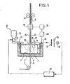
- Figure 1 a crucible 1 of silica, the outer walls of which are surrounded by a furnace 2 which may for example be of the induction type.
- the crucible 1 contains a bath 3 of molten silicon with the balance of t surface rises in the crucible at a level H.
- the bottom of the crucible 1 has a calibrated slot 4 through which vertically pass 5 carbon ribbon that passes vertically the equilibrium surface of the bath 3.
- Mechanical means 6 and 7 are provided for moving the strip 5 from bottom to top in the direction of the arrow 8.
- An electromechanical system 9 placed on the edge of the crucible 1 makes it possible to supply the latter with solid silicon.
- the system 9 essentially comprises a reservoir 10 of calibrated silicon pellets, a conduit 11 inclined towards the interior of the crucible and an electromechanical distribution member 12 mechanically connecting the reservoir 10 and the conduit 11.
- An optical system shown diagrammatically by a simple converging lens 13 associated with a diaphragm 14, is centered on an axis 15 fixed relative to the crucible and situated a little above the level of the bath 3.
- the electrical output of a photoelectric detector 16 disposed on the axis 15 is connected through a servo system 17 to the electrical control of the distribution member 12.
- the detector 16 can be, for example, constituted by a solar cell.
- a thickness measuring device 18 surrounds the tape 5 at the outlet of the bath 3. This device 18 is connected through another assertion circuit. 7 ordinance 19 and a control circuit 20 at the electrical input of Pour 2.
- the device shown in Figure 1 operates as follows.
- the means 6-7 for moving the ribbon 5 being on so as to make it circulate at constant speed in the bath it can be seen that the equilibrium level of the bath rises near each face of the ribbon to form two menisci 21 and 22, while two layers 23 and 24 of polycrystalline silicon are deposited on the faces of the ribbon 5 at the outlet of the bath 3.
- a line is established connection 25, end view in Figure 1. This line is located at the upper end of the meniscus 21, at a height h above the level of the bath.
- This rise in level h is due to capillarity phenomena. It is practically independent of the level as well as the temperature of the bath and can therefore be considered as constant.
- the supply system 9 slides silicon wafers, one by one, over the pipe 11, one by one, at a rate which is controlled by the electrical signal supplied by the servo system 17 to the electromechanical distribution unit 12.
- the optical system 13-14 is fixed near the crucible 1, so that its axis 15 intersects the connection line 25 when the bath is at a level H at which it is desired to stabilize it.
- the lens 13 forms on the sensitive surface of the detector 16 the image of a small area of the silicon surface located on either side of the connection line 25, this area being delimited by the diaphragm 14.
- the axis 15 of the optical system can be horizontal as shown in FIG. 1, or slightly inclined relative to the horizontal so that the edge of the crucible does not mask the image of the small area on the detector 16.
- the part of this image which corresponds to liquid silicon is much darker than that which corresponds to solid silicon, because liquid silicon has a much lower luminosity than that of solid silicon at near the melting point.
- the detector 16 delivers a signal whose amplitude is directly a function of the illumination it receives. This signal therefore varies when the line separating the two parts of the image moves over the sensitive surface of the detector.
- any variation in the level of the bath results in an equal variation and in the same direction in the level of the connection line 25; this variation in the level of line 25 causes a corresponding variation in the electrical signal delivered by the receiver 16.
- the servo system 17 compares this electrical signal with a reference signal to form an error signal.
- the system 17 controls the rate of distribution of the silicon pellets so as to reduce this error signal.
- the device illustrated in FIG. 1 therefore makes it possible to stabilize the level of the bath at a predetermined value.
- the thickness of the polycrystalline silicon layer deposited on the ribbon 5 varies with the temperature of the bath, from a few micrometers per degree C.
- the temperature of the bath varies according to the level of the bath, substantially 3 degrees C per millimeter.
- the device described above makes it possible to avoid the variations in temperature of the bath caused by fluctuations in its level. Therefore, if the temperature of the bath is varied by acting on the heat given off by the oven 2, we can now adjust the thickness of the layer of silicon deposited on the carbon ribbon.
- the measuring device 18 which can be for example an X-ray or gamma ray probe, or a capacitive probe, delivers an electrical measurement signal representative of the thickness of the deposited silicon layer.
- the servo system 19 compares this signal to a reference signal and controls through the circuit 20 the power delivered by the oven 2 so as to reduce the difference between the measurement signal and the reference signal.
- the servo system may include means for varying the reference signal, so as to control a corresponding variation in the thickness of silicon deposited.
- FIG. 2 schematically shows the elements that an optical sighting system for the connection line 25 can include.
- represented system comprises, successively aligned on the axis 15, from the line 25 to the detector 16, filters 26, a lens 27, an optical recovery system 28, an eyepiece 29 and the diaphragm 14.
- an optical reflective blade 30 partially inclined at 45 degrees on the axis 15 is disposed, in order to return along an axis 31 part of the light coming from the zone targeted on the line 25.
- An eyepiece 32 comprising a reticle 33 is centered on the axis 31 so as to allow the eye 34 of an operator to observe the target area.
- the electrical output of the photoelectric detector is connected directly to the input of the servo system.
- the detector's electrical output signal is proportional to the light energy from the target area and illuminating the photosensitive surface of the detector. This energy is representative of the level of the silicon bath in the crucible.
- the light power of the targeted zone can vary over time, independently of the level of the bath, for various reasons, in particular when the temperature of the silicon located in said zone varies. These variations in light power then cause disturbances in the regulation of the level of the silicon bath.
- the device shown in FIG. 3 makes it possible to prevent the regulation of the level of the silicon bath from being disturbed by variations in the light power emitted by the targeted area.
- a crucible 1 is shown in silica, the outer walls of which are surrounded by an oven 2 which may be of the induction type.
- the crucible 1 contains a bath 3 of molten silicon, the equilibrium surface of which rises in the crucible at a level H.
- the bottom of the crucible 1 has a calibrated slot 4 through which a carbon ribbon 5 which passes vertically passes through vertically the equilibrium surface of the bath 3. Rollers 6 and 7 allow the ribbon 5 to be moved from bottom to top in the direction of arrow 8.
- An electromechanical system 9 is placed on the edge of the crucible 1 to supply it with solid silicon.
- the system 9 essentially comprises a reservoir 10 of silicon pellets, a conduit 11 inclined towards the interior of the crucible and an electromechanical member for distribution 12 mechanically connecting the reservoir 10 and the conduit 11.
- a photoelectric detector comprising an assembly 35 of two photoelectric cells and a processing system 36 whose input is connected to the electrical outputs of the two cells.
- the output of the processing system 36 is connected, through a servo system 17, to the electrical control of the distribution member 12.
- a thickness measuring device 18 surrounds the tape 5 at the outlet of the bath 3.
- the device 18 is connected, through another servo system 19 and a control circuit 20, to the electrical inlet of the oven 2 .
- FIG. 4 is a diagram of the photoelectric detector formed by the assembly 35 of the two cells and by the processing system 36 connected to this assembly.
- These cells are solar cells 37 and 38.
- the electrical outputs of the solar cell 37 are connected to the input of a current-voltage converter 39; similarly the electrical outputs of the photocell 38 are connected to the input of a converter 40 analogous to the converter 39, these converters being part of the system 36.
- the outputs of the two converters 39 and 40 are connected on the one hand to the two respectively inputs of a subtractor circuit 41 and on the other hand to the two inputs of a summing circuit 42.
- the outputs of the subtracting and summing circuits are connected respectively to the two inputs of a dividing circuit 43 whose output constitutes that of the processing system 36.
- FIG. 5 shows the photosensitive surfaces 44 and 45 of the two solar cells 37 and 38 forming the assembly 35.
- the surfaces 44 and 45 are in the form of an isosceles right triangle and are juxtaposed in a plane on either side of a line of separation 46 which is parallel to the long side of each triangle and very close to these sides. All of these two cells can be obtained by forming, by photogravure, a narrow groove in the junction area of a square-shaped solar cell, this groove being located along the diagonal of the square.
- the means 6-7 for moving the ribbon 5 being on so as to make it circulate at constant speed in the bath it can be seen that the equilibrium level of the bath rises near each face of the ribbon to form two menisci 21 and 22, while two layers 23 and 24 of polycrystalline silicon are deposited on the faces of the ribbon 5 at the outlet of the bath 3.
- a line is established connection 25, end view in FIG. 1. This line is located at the upper end of the meniscus 21, at a height h above the level of the bath.
- the rise in level h is due to capillarity phenomena. It is practically independent of the level as well as the temperature of the bath and can therefore be considered as constant.
- the rib of the solid-liquid connection line 25 is in direct relation with the level of the bath H.
- the supply system 9 slides silicon wafers, one by one, over the pipe 11, one by one, at a rate which is controlled by the electrical signal supplied by the servo system 17 to the electromechanical distribution unit 12.
- the optical system 13-14 is fixed near the crucible 1, so that its axis 15 intersects the connection line 25 when the bath is at. a level H at which one wishes to stabilize it.
- the lens 13 forms on the receiving surface of the assembly 35 the image of a small area of the surface of the silicon situated on either side of the connection line 25, this area being delimited by the diaphragm 14.
- the axis 15 of the optical system can be horizontal as shown in FIG. 3, or slightly inclined relative to the horizontal so that the edge of the crucible does not mask the image of the small area.
- the plane of the photosensitive surfaces 44 and 45 is perpendicular to the plane of Figure 3 and the center of the square forming the receiving surface of the assembly 35 is located on the axis 15.
- This square is oriented in its plane so that the line image connection 25 on the receiving surface cuts the separation line 46 at an angle other than 90 °, preferably at an angle of 45 degrees, this angle corresponding to the greatest sensitivity of the system.
- this image 47 passes through the trace of the axis 15 on the receiving surface since the axis 15 intersects the connection line 25 (FIG. 3).
- the part of the reception surface situated below the line 47 corresponds to the liquid silicon of the small area. This part, hatched in FIG. 5, is much less illuminated than that situated above the line 47 because the liquid silicon has a much lower luminosity than that of solid silicon near its melting temperature.
- each cell 37, 38 delivers a current proportional to the total flux it receives, this current being transformed by the converter connected to its output into a voltage signal A, B.
- the receiving surface of the assembly 35 comprises two ranges, a first area receiving the radiation of liquid silicon and a second area illuminated by solid silicon with a power P, the contrast between the illumination of these two areas being of the order of 1/20. We can therefore admit that, for each cell, the current delivered corresponding to the first range is negligible compared to that corresponding to the second range.
- Each signal A or B is therefore substantially proportional to P and to the area of the second range of the cell.
- the output signal from the processing circuit 36 which is equal to , is representative of the level of the connection line and therefore of the level of the molten silicon bath since the value of h is constant.
- the servo system 17 compares the electrical signal delivered by the processing circuit 36 with a reference signal to form an error signal, and controls the rate of distribution of the silicon wafers so as to reduce this error signal.
- the device illustrated in FIG. 3 therefore makes it possible to stabilize the level of the bath at a predetermined value.
- the thickness of the polycrystalline silicon layer deposited on the ribbon 5 varies with the temperature of the bath, from a few micrometers per degree C.
- the temperature of the bath varies according to the level of the bath, substantially 3 degrees C per millimeter.
- the device described above makes it possible to avoid the variations in temperature of the bath caused by fluctuations in its level. Therefore, if the temperature of the bath is varied by acting on the heat given off by the oven 2, the thickness of the layer of silicon deposited on the carbon ribbon can be adjusted.
- the measuring device 18 which can for example be an X-ray or gamma ray probe, a capacitive probe, or a differential system of mechanical probes, delivers an electrical measurement signal representative of the thickness of the layer. of deposited silicon.
- the servo system 19 compares this signal to a reference signal and controls through the circuit 20 the power delivered by the oven 2 so as to reduce the difference between the measurement signal and the reference signal.
- the servo system 19 may include means for varying the reference signal, so as to control a corresponding variation in the thickness of silicon deposited.
- the electrical output signal from the processing system 36 is independent of the power P of the silicon radiation, and therefore independent of the variations of this power P as a function of time. It appears, in fact, that the power P can vary over time, either as a result of variations in the temperature of the silicon, or as a result of variations in the homogeneity of the silicon, or as a result of variations in the light emission lobe of the silicon caused by a deformation of the carbon ribbon.
- the device according to the invention therefore makes it possible to regulate the level of the molten silicon bath without being hampered by variations in the light power P.
- the device described above can be applied to the mass production of solar cells.
Landscapes
- Chemical & Material Sciences (AREA)
- Engineering & Computer Science (AREA)
- Crystallography & Structural Chemistry (AREA)
- Materials Engineering (AREA)
- Metallurgy (AREA)
- Organic Chemistry (AREA)
- Silicon Compounds (AREA)
- Liquid Deposition Of Substances Of Which Semiconductor Devices Are Composed (AREA)
- Photovoltaic Devices (AREA)
Priority Applications (1)
| Application Number | Priority Date | Filing Date | Title |
|---|---|---|---|
| AT84110062T ATE37449T1 (de) | 1983-08-29 | 1984-08-23 | Vorrichtung zum kontinuierlichen niederschlagen einer schicht aus polykristallinem silizium auf einem kohlenstoffband. |
Applications Claiming Priority (4)
| Application Number | Priority Date | Filing Date | Title |
|---|---|---|---|
| FR8313834A FR2551233B1 (fr) | 1983-08-29 | 1983-08-29 | Dispositif pour deposer en regime continu une couche de silicium polycristallin sur un ruban de carbone |
| FR8313834 | 1983-08-29 | ||
| FR8319212A FR2556109B2 (fr) | 1983-08-29 | 1983-12-01 | Dispositif pour deposer en regime continu une couche de silicium polycristallin sur un ruban de carbone |
| FR8319212 | 1983-12-01 |
Publications (2)
| Publication Number | Publication Date |
|---|---|
| EP0141114A1 true EP0141114A1 (de) | 1985-05-15 |
| EP0141114B1 EP0141114B1 (de) | 1988-09-21 |
Family
ID=26223566
Family Applications (1)
| Application Number | Title | Priority Date | Filing Date |
|---|---|---|---|
| EP84110062A Expired EP0141114B1 (de) | 1983-08-29 | 1984-08-23 | Vorrichtung zum kontinuierlichen Niederschlagen einer Schicht aus polykristallinem Silizium auf einem Kohlenstoffband |
Country Status (6)
| Country | Link |
|---|---|
| US (1) | US4577588A (de) |
| EP (1) | EP0141114B1 (de) |
| AU (1) | AU564654B2 (de) |
| CA (1) | CA1224026A (de) |
| DE (1) | DE3474222D1 (de) |
| FR (1) | FR2556109B2 (de) |
Cited By (1)
| Publication number | Priority date | Publication date | Assignee | Title |
|---|---|---|---|---|
| FR2896254A1 (fr) * | 2006-01-17 | 2007-07-20 | Solarforce Soc Par Actions Sim | Tirage symetrique de rubans composites |
Families Citing this family (12)
| Publication number | Priority date | Publication date | Assignee | Title |
|---|---|---|---|---|
| FR2592064B1 (fr) * | 1985-12-23 | 1988-02-12 | Elf Aquitaine | Dispositif pour former un bain d'un materiau semi-conducteur fondu afin d'y faire croitre un element cristallin |
| JPS62151358A (ja) * | 1985-12-26 | 1987-07-06 | Toshiba Corp | サ−マルヘツド |
| US4910453A (en) * | 1987-10-15 | 1990-03-20 | Ade Corporation | Multi-probe grouping system with nonlinear error correction |
| US5047386A (en) * | 1988-12-29 | 1991-09-10 | Troy Investments Inc. | Apparatus for continuous manufacture of high temperature superconducting wires from molten superconducting oxides |
| TW324788B (en) * | 1995-10-06 | 1998-01-11 | Sumitomo Electric Industries | Coating apparatuse for optical fiber |
| US6200383B1 (en) * | 1999-05-03 | 2001-03-13 | Evergreen Solar, Inc. | Melt depth control for semiconductor materials grown from a melt |
| DE10146791A1 (de) * | 2001-09-20 | 2003-04-10 | Sms Demag Ag | Verfahren und Vorrichtung zum Beschichten der Oberfläche von strangförmigem metallischem Gut |
| DE60316337T2 (de) * | 2002-10-18 | 2008-06-05 | Evergreen Solar Inc., Marlborough | Verfahren und vorrichtung zur kristallzüchtung |
| US6814802B2 (en) * | 2002-10-30 | 2004-11-09 | Evergreen Solar, Inc. | Method and apparatus for growing multiple crystalline ribbons from a single crucible |
| DE10254306A1 (de) * | 2002-11-21 | 2004-06-03 | Sms Demag Ag | Verfahren und Vorrichtung zur Schmelztauchbeschichtung eines Metallstranges |
| NL1026043C2 (nl) * | 2004-04-26 | 2005-10-27 | Stichting Energie | Werkwijze en inrichting voor het fabriceren van metalen folies. |
| KR101314668B1 (ko) * | 2012-02-07 | 2013-10-04 | 최대규 | 소재의 가공장치 |
Citations (10)
| Publication number | Priority date | Publication date | Assignee | Title |
|---|---|---|---|---|
| FR2034975A1 (de) * | 1969-03-17 | 1970-12-18 | Hamco Mach & Elect Co | |
| US3730962A (en) * | 1971-08-24 | 1973-05-01 | Airco Inc | Electron beam furance with material-evaporant equilibrium control |
| US3738312A (en) * | 1971-12-28 | 1973-06-12 | Bethlehem Steel Corp | Molten metal bath level maintenance system |
| US3740563A (en) * | 1971-06-25 | 1973-06-19 | Monsanto Co | Electroptical system and method for sensing and controlling the diameter and melt level of pulled crystals |
| US3998598A (en) * | 1973-11-23 | 1976-12-21 | Semimetals, Inc. | Automatic diameter control for crystal growing facilities |
| FR2323645A1 (fr) * | 1975-09-15 | 1977-04-08 | Pilkington Brothers Ltd | Procede pour la fabrication d'une tige en verre revetue d'une couche d'un autre verre |
| FR2446333A1 (fr) * | 1979-01-15 | 1980-08-08 | Mobil Tyco Solar Energy Corp | Appareil et procede pour controler la croissance d'un corps cristallin |
| US4217165A (en) * | 1978-04-28 | 1980-08-12 | Ciszek Theodore F | Method of growing a ribbon crystal particularly suited for facilitating automated control of ribbon width |
| EP0048688A2 (de) * | 1980-08-27 | 1982-03-31 | Cables Cortaillod S.A. | Verfahren zur optischen Detektion und/oder zum Messen einer Deformation und/oder einer Versetzung eines Objektes oder eines Objektteiles, Vorrichtung für die Ausführung dieses Verfahrens und Anwendung des Verfahrens |
| US4410270A (en) * | 1981-04-20 | 1983-10-18 | Litton Systems, Inc. | Angle position transducer |
Family Cites Families (3)
| Publication number | Priority date | Publication date | Assignee | Title |
|---|---|---|---|---|
| FR2386359A1 (fr) * | 1977-04-07 | 1978-11-03 | Labo Electronique Physique | Procede de depot par immersion en continu, dispositif et produits obtenus |
| US4246868A (en) * | 1979-07-13 | 1981-01-27 | Westvaco Corporation | Envelope machine gum box |
| US4383130A (en) * | 1981-05-04 | 1983-05-10 | Alpha Solarco Inc. | Solar energy cell and method of manufacture |
-
1983
- 1983-12-01 FR FR8319212A patent/FR2556109B2/fr not_active Expired
-
1984
- 1984-08-20 CA CA000461389A patent/CA1224026A/fr not_active Expired
- 1984-08-23 DE DE8484110062T patent/DE3474222D1/de not_active Expired
- 1984-08-23 EP EP84110062A patent/EP0141114B1/de not_active Expired
- 1984-08-28 US US06/644,910 patent/US4577588A/en not_active Expired - Fee Related
- 1984-08-28 AU AU32469/84A patent/AU564654B2/en not_active Ceased
Patent Citations (10)
| Publication number | Priority date | Publication date | Assignee | Title |
|---|---|---|---|---|
| FR2034975A1 (de) * | 1969-03-17 | 1970-12-18 | Hamco Mach & Elect Co | |
| US3740563A (en) * | 1971-06-25 | 1973-06-19 | Monsanto Co | Electroptical system and method for sensing and controlling the diameter and melt level of pulled crystals |
| US3730962A (en) * | 1971-08-24 | 1973-05-01 | Airco Inc | Electron beam furance with material-evaporant equilibrium control |
| US3738312A (en) * | 1971-12-28 | 1973-06-12 | Bethlehem Steel Corp | Molten metal bath level maintenance system |
| US3998598A (en) * | 1973-11-23 | 1976-12-21 | Semimetals, Inc. | Automatic diameter control for crystal growing facilities |
| FR2323645A1 (fr) * | 1975-09-15 | 1977-04-08 | Pilkington Brothers Ltd | Procede pour la fabrication d'une tige en verre revetue d'une couche d'un autre verre |
| US4217165A (en) * | 1978-04-28 | 1980-08-12 | Ciszek Theodore F | Method of growing a ribbon crystal particularly suited for facilitating automated control of ribbon width |
| FR2446333A1 (fr) * | 1979-01-15 | 1980-08-08 | Mobil Tyco Solar Energy Corp | Appareil et procede pour controler la croissance d'un corps cristallin |
| EP0048688A2 (de) * | 1980-08-27 | 1982-03-31 | Cables Cortaillod S.A. | Verfahren zur optischen Detektion und/oder zum Messen einer Deformation und/oder einer Versetzung eines Objektes oder eines Objektteiles, Vorrichtung für die Ausführung dieses Verfahrens und Anwendung des Verfahrens |
| US4410270A (en) * | 1981-04-20 | 1983-10-18 | Litton Systems, Inc. | Angle position transducer |
Non-Patent Citations (1)
| Title |
|---|
| PATENTS ABSTRACTS OF JAPAN, vol. 3, no. 55(C-45), 11 mai 1979, page 69C45; & JP - A - 54 29843 (SHIN NIPPON SEITETSU K.K.) 03-06-1979 * |
Cited By (2)
| Publication number | Priority date | Publication date | Assignee | Title |
|---|---|---|---|---|
| FR2896254A1 (fr) * | 2006-01-17 | 2007-07-20 | Solarforce Soc Par Actions Sim | Tirage symetrique de rubans composites |
| WO2007083044A1 (fr) * | 2006-01-17 | 2007-07-26 | Solarforce | Tirage symétrique de rubans composites |
Also Published As
| Publication number | Publication date |
|---|---|
| FR2556109B2 (fr) | 1986-09-12 |
| AU3246984A (en) | 1985-03-07 |
| US4577588A (en) | 1986-03-25 |
| CA1224026A (fr) | 1987-07-14 |
| DE3474222D1 (en) | 1988-10-27 |
| EP0141114B1 (de) | 1988-09-21 |
| FR2556109A2 (fr) | 1985-06-07 |
| AU564654B2 (en) | 1987-08-20 |
Similar Documents
| Publication | Publication Date | Title |
|---|---|---|
| EP0141114B1 (de) | Vorrichtung zum kontinuierlichen Niederschlagen einer Schicht aus polykristallinem Silizium auf einem Kohlenstoffband | |
| US4589773A (en) | Position detecting system | |
| US7837383B2 (en) | Apparatus and method for real time measurement of substrate temperatures for use in semiconductor growth and wafer processing | |
| FR2817339A1 (fr) | Dispositif de relevement tridimensionnel d'une scene a emission laser | |
| FR2488689A1 (fr) | Procede et appareil pour controler le diametre des fibres de verre en cours de fabrication | |
| JPH06167456A (ja) | スキャナの校正方法及び所定の散乱光振幅の発生装置 | |
| CH643618A5 (fr) | Machine de chantier ferroviaire. | |
| EP0597530A1 (de) | Volumendurchflussmesser zum Messen der Flugzeit | |
| FR2500696A1 (fr) | Recepteur optique | |
| US2879691A (en) | Photoelectric exposure meter | |
| FR2553538A1 (fr) | Procede et dispositif permettant le reglage du chauffage d'une enceinte thermostatee d'un oscillateur notamment a quartz | |
| CA2064451C (en) | Radiometer with correction device | |
| US3995073A (en) | Method for thermal deposition of metal | |
| FR2551233A1 (fr) | Dispositif pour deposer en regime continu une couche de silicium polycristallin sur un ruban de carbone | |
| US4726680A (en) | Absorbance monitor | |
| WO2004013619A2 (fr) | Procede et dispositif de mesure en ligne de caracteristiques d'un revetement de surface d'un produit metallurgique | |
| US5239359A (en) | Absorbance monitor | |
| EP0528702B1 (de) | Abbildungssystem mit integrierter Abnutzungsmessung der in Transmission arbeitenden optischen Elemente und optronische Abbildungseinrichtung, bestehend aus solch einem Abbildungssystem | |
| FR2822967A1 (fr) | Dispositif pour insoler une face d'un panneau de circuit imprime | |
| US4046100A (en) | Apparatus for thermal deposition of metal | |
| JP2787133B2 (ja) | 照明光学装置 | |
| JPH11316351A (ja) | セラミック補間フィルタ | |
| JP7291723B2 (ja) | 材料層の厚さを決定するための測定装置 | |
| FR2680240A1 (fr) | Procede de mesure en continu de l'epaisseur d'un film d'huile sur la surface d'une tole en defilement dans une installation de laminage a froid. | |
| JPH10206527A (ja) | 干渉フィルタ温度制御装置およびレーザレーダ装置 |
Legal Events
| Date | Code | Title | Description |
|---|---|---|---|
| PUAI | Public reference made under article 153(3) epc to a published international application that has entered the european phase |
Free format text: ORIGINAL CODE: 0009012 |
|
| AK | Designated contracting states |
Designated state(s): AT BE CH DE FR GB IT LI LU NL SE |
|
| 17P | Request for examination filed |
Effective date: 19851029 |
|
| 17Q | First examination report despatched |
Effective date: 19870330 |
|
| GRAA | (expected) grant |
Free format text: ORIGINAL CODE: 0009210 |
|
| AK | Designated contracting states |
Kind code of ref document: B1 Designated state(s): AT BE CH DE FR GB IT LI LU NL SE |
|
| REF | Corresponds to: |
Ref document number: 37449 Country of ref document: AT Date of ref document: 19881015 Kind code of ref document: T |
|
| REF | Corresponds to: |
Ref document number: 3474222 Country of ref document: DE Date of ref document: 19881027 |
|
| GBT | Gb: translation of ep patent filed (gb section 77(6)(a)/1977) | ||
| ITF | It: translation for a ep patent filed | ||
| PLBE | No opposition filed within time limit |
Free format text: ORIGINAL CODE: 0009261 |
|
| STAA | Information on the status of an ep patent application or granted ep patent |
Free format text: STATUS: NO OPPOSITION FILED WITHIN TIME LIMIT |
|
| PG25 | Lapsed in a contracting state [announced via postgrant information from national office to epo] |
Ref country code: GB Effective date: 19890823 Ref country code: AT Effective date: 19890823 |
|
| PG25 | Lapsed in a contracting state [announced via postgrant information from national office to epo] |
Ref country code: SE Effective date: 19890824 |
|
| PG25 | Lapsed in a contracting state [announced via postgrant information from national office to epo] |
Ref country code: LU Free format text: LAPSE BECAUSE OF NON-PAYMENT OF DUE FEES Effective date: 19890831 Ref country code: LI Effective date: 19890831 Ref country code: CH Effective date: 19890831 Ref country code: BE Effective date: 19890831 |
|
| 26N | No opposition filed | ||
| BERE | Be: lapsed |
Owner name: SOC. NATIONALE ELF AQUITAINE Effective date: 19890831 Owner name: CIE GENERALE D' ELECTRICITE Effective date: 19890831 |
|
| PG25 | Lapsed in a contracting state [announced via postgrant information from national office to epo] |
Ref country code: NL Effective date: 19900301 |
|
| NLV4 | Nl: lapsed or anulled due to non-payment of the annual fee | ||
| GBPC | Gb: european patent ceased through non-payment of renewal fee | ||
| PG25 | Lapsed in a contracting state [announced via postgrant information from national office to epo] |
Ref country code: FR Effective date: 19900427 |
|
| REG | Reference to a national code |
Ref country code: CH Ref legal event code: PL |
|
| PG25 | Lapsed in a contracting state [announced via postgrant information from national office to epo] |
Ref country code: DE Effective date: 19900501 |
|
| REG | Reference to a national code |
Ref country code: FR Ref legal event code: ST |
|
| EUG | Se: european patent has lapsed |
Ref document number: 84110062.1 Effective date: 19900418 |