EP0141193A1 - Dispositif enfichable comprenant une rangée de fiches et une rangée de prises coopérantes - Google Patents
Dispositif enfichable comprenant une rangée de fiches et une rangée de prises coopérantes Download PDFInfo
- Publication number
- EP0141193A1 EP0141193A1 EP84110910A EP84110910A EP0141193A1 EP 0141193 A1 EP0141193 A1 EP 0141193A1 EP 84110910 A EP84110910 A EP 84110910A EP 84110910 A EP84110910 A EP 84110910A EP 0141193 A1 EP0141193 A1 EP 0141193A1
- Authority
- EP
- European Patent Office
- Prior art keywords
- socket
- plug
- strip
- contacts
- contact
- Prior art date
- Legal status (The legal status is an assumption and is not a legal conclusion. Google has not performed a legal analysis and makes no representation as to the accuracy of the status listed.)
- Withdrawn
Links
- 230000013011 mating Effects 0.000 claims abstract description 42
- 238000003780 insertion Methods 0.000 claims abstract description 8
- 230000037431 insertion Effects 0.000 claims abstract description 8
- 230000003247 decreasing effect Effects 0.000 claims abstract 3
- 238000005476 soldering Methods 0.000 claims description 8
- 230000000295 complement effect Effects 0.000 claims description 5
- 239000012777 electrically insulating material Substances 0.000 claims description 3
- 241000446313 Lamella Species 0.000 description 10
- 238000000034 method Methods 0.000 description 5
- 238000003466 welding Methods 0.000 description 4
- 238000010276 construction Methods 0.000 description 2
- 230000008878 coupling Effects 0.000 description 2
- 238000010168 coupling process Methods 0.000 description 2
- 238000005859 coupling reaction Methods 0.000 description 2
- 230000007423 decrease Effects 0.000 description 2
- 238000004519 manufacturing process Methods 0.000 description 2
- 229910000679 solder Inorganic materials 0.000 description 2
- 238000003892 spreading Methods 0.000 description 2
- 238000009423 ventilation Methods 0.000 description 2
- 238000005452 bending Methods 0.000 description 1
- 230000015572 biosynthetic process Effects 0.000 description 1
- 238000010292 electrical insulation Methods 0.000 description 1
- 238000009413 insulation Methods 0.000 description 1
- 230000001681 protective effect Effects 0.000 description 1
Images


Classifications
-
- H—ELECTRICITY
- H01—ELECTRIC ELEMENTS
- H01R—ELECTRICALLY-CONDUCTIVE CONNECTIONS; STRUCTURAL ASSOCIATIONS OF A PLURALITY OF MUTUALLY-INSULATED ELECTRICAL CONNECTING ELEMENTS; COUPLING DEVICES; CURRENT COLLECTORS
- H01R24/00—Two-part coupling devices, or either of their cooperating parts, characterised by their overall structure
- H01R24/60—Contacts spaced along planar side wall transverse to longitudinal axis of engagement
-
- H—ELECTRICITY
- H01—ELECTRIC ELEMENTS
- H01R—ELECTRICALLY-CONDUCTIVE CONNECTIONS; STRUCTURAL ASSOCIATIONS OF A PLURALITY OF MUTUALLY-INSULATED ELECTRICAL CONNECTING ELEMENTS; COUPLING DEVICES; CURRENT COLLECTORS
- H01R12/00—Structural associations of a plurality of mutually-insulated electrical connecting elements, specially adapted for printed circuits, e.g. printed circuit boards [PCB], flat or ribbon cables, or like generally planar structures, e.g. terminal strips, terminal blocks; Coupling devices specially adapted for printed circuits, flat or ribbon cables, or like generally planar structures; Terminals specially adapted for contact with, or insertion into, printed circuits, flat or ribbon cables, or like generally planar structures
- H01R12/70—Coupling devices
- H01R12/71—Coupling devices for rigid printing circuits or like structures
- H01R12/72—Coupling devices for rigid printing circuits or like structures coupling with the edge of the rigid printed circuits or like structures
- H01R12/722—Coupling devices for rigid printing circuits or like structures coupling with the edge of the rigid printed circuits or like structures coupling devices mounted on the edge of the printed circuits
- H01R12/727—Coupling devices presenting arrays of contacts
Definitions
- the invention relates to a connector assembly of the type mentioned in the preamble of claim 1.
- Such connector arrangements are used primarily for the electrical connection of printed circuit boards with electrical devices.
- the socket strip is generally arranged on an edge of the circuit board, while the plug strip is connected to the device.
- Several contacts staggered in the direction of insertion allow a high contact density on the given edge length of the circuit board.
- a problem with such connector arrangements is that, for example, the front mating contact of the connector strip passes all contacts of the socket strip in succession until it reaches the contact assigned to it. There is a risk that incorrect contacts will occur, which can damage the circuit board or the device. Care must therefore be taken to ensure that incorrect contacts are avoided when inserting or removing a circuit board from the device.
- a connector arrangement of the generic type is already known, in which the contacts of the socket strip are arranged in pairs opposite one another in such a way that all the sockets formed by two opposite contacts each have the same socket width (US Pat. No. 4,288,140).
- all contacts of the socket strip are assigned cams, which by the circuit board itself can be confirmed when plugging in or removing; these cams spread the sockets so far that no contact between the contacts of the socket strip and the mating contacts of the connector strip can take place. Only when the plug-in card assumes a position in which the assigned contacts and mating contacts face each other, do the cams release the contacts forming the sockets, so that the contacts spring into their natural position and thereby come into contact with the mating contacts.
- the contacts of the sockets and the mating contacts of the plugs are graded so that the small thickness of the front plug part in the plug direction first passes through the socket parts of the large socket width until it reaches the the part of the socket assigned to it arrives; At this moment, all other connector parts also reach the socket parts assigned to them, corresponding to the socket width, so that all assigned contacts or counter-contacts come into mutual contact at the same time.
- centering guides are provided which prevent mutual tilting during the plugging or unplugging.
- each socket therefore consists of several two-pole socket parts arranged one behind the other in the plug-in direction with a socket width that decreases in the plug-in direction; the plugs have a corresponding, complementary profile with a plurality of two-pole plug parts, the thickness of which decreases in the direction of insertion.
- the contacts of the socket strip and the mating contacts of the plug strip are preferably each formed by a plurality of contact lamellae lying flat one above the other and oriented in the plugging direction, one end of which is connected to the electrical components of the associated devices, while the other end forms the contact zones.
- the construction of the socket strip or the connector strip is carried out according to the invention in such a way that the contact lamellae of the socket strip and / or the contact lamellae of the connector strip are each mounted on common support bodies made of electrically insulating material and that the socket strips or connector strips formed in this way are each in a socket housing or a plug housing can be used which protects the contacts against any external contact.
- the socket strip and the connector strip are each arranged with a certain movement in the housings, so that a mutual movement of the socket strip or connector strip, which is not always exactly aligned with one another, is possible during the plugging process.
- the contact lamellae of the plug connector are designed as soldering lugs on their connection ends facing away from the contact side and are shaped into an elastic movement compensation curve between their connection end and their area connected to the supporting bodies.
- the forces acting on the connection ends during assembly or operation of the device are absorbed by the movement compensation bend, so that the exact position of the contact ends cannot be influenced.
- a ground plug projecting up to the level of the front counter contact in the plug-in direction with a thickness corresponding to the greatest plug thickness is arranged on the plug strip and that a ground socket opposite the ground plug is arranged on the socket strip, which only the corresponding contacts have the largest socket width.
- the socket housing and the plug housing are each advanced approximately to the level of the front contacts and that one of the housings has an outer contour corresponding to the inner contour of the other housing. Plugging is therefore only possible if the two housings and thus the connector strip and the socket strip are exactly aligned with one another, so that incorrect contacts due to canting are excluded.
- the socket strip and the plug strip are each provided with complementary guiding surfaces which ensure that they are plugged together in the correct position and orientation.
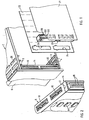
- the device housing 2 shown in a view from the rear in FIG. 1 is provided with a plurality of compartments 4 formed by small webs 3 for accommodating slide-in housings 6, in each of which a printed circuit board is arranged. For better clarity, only a few compartments 4 and only one slide-in housing 6 are shown.
- FIG. 2 shows a slide-in housing 6 with a printed circuit board 10 arranged therein and equipped with electronic components 8.
- the rear of the device can be attached side facing narrow side 12 of the slide-in housing 6, a contact lamella unit 14 can be attached, the contact lamellae 16 of which are each connected to edge contacts arranged on the edge of the plate 12 assigned to the narrow edge.
- the slide-in housing 6 is equipped with ventilation slots 18 which each cover ventilation slots 20 formed in the top and bottom of the device housing 2.
- the contact lamellae 16 come into electrically conductive connection with mating contacts contained in the mating contact units 26.
- Each of the mating contacts ends on the back of the mating contact unit as a soldering tab 108 or the like, which are interconnected in a manner known per se via a so-called electrical rear wall 31.
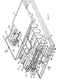
- FIG. 3 shows a contact lamella unit 14, which is attached to the slide-in housing 6, in a viewing direction that has been changed compared to FIG. 1.
- the circuit board 10 is arranged in the slide-in housing 6 and fastened in a manner not shown in detail.
- edge sections are provided with groups of contact points 28a to 28d, which are arranged approximately at right angles to the plate edge 25 and are connected in a manner not shown to the electronic components on the printed circuit board 10.
- contact points 28a to 28d are each assigned contact lamellae 30a to 30d, which have a first end 32a to 32d in electrical contact with these contact points and whose free leg 34a to 34d facing away from the first end is aligned parallel to the printed circuit board 10 and in the direction of insertion .
- the free legs 34a to 34d of the contact blades 30a to 30d of a contact blade group lie one above the other in one plane. In this way, several edge contacts can be assigned to each edge section of the printed circuit board 10, which leads to an increase in the possible number of contacts for a given edge length.
- the free ends of the contact lamellae 30a to 30d are not all one above the other, but are partially offset from one another in the direction of insertion.
- the two outer contact plates 30a and 30d are combined to form an outer, two-pole socket part 36, the inner contact plates 30b and 30c to form an inner, two-pole socket part 38.
- the inner socket part 38 is set back in the direction of insertion (arrow 40) relative to the outer socket part 36; both socket parts together form a socket 35.
- all contact lamellae which form the contact sockets in the exemplary embodiment described are on common Carrying bodies 42, 44, 46 and supporting bodies 64, 66 assembled from an electrically insulating material and combined to form a socket strip 48.
- the support bodies 42 to 46 and the support bodies 64, 66 can be mechanically connected to one another in a manner not shown, for example by ultrasonic welding.
- the socket strip 48 is received as a whole in a protective socket housing 50.
- the contact lamella unit 14 is therefore composed of the socket strip 48 and the socket housing 50.
- the support bodies 42 to 46 isolate the individual contact lamellae from one another and give them a certain rigidity so that they are protected against bending.
- the support bodies 42, 44, 46 are each provided with retaining cams 52, 54, 56 which engage in corresponding recesses (for example 58) in the contact lamellae and connect these to the support bodies.
- supporting bodies 60 are fastened to their inner sides, which on the one hand also serve to stiffen these contact lamellae and on the other hand as support for the inner contact lamellae 30b and 30c via the retaining lugs 61 formed on them are each provided on the support bodies intermediate webs 62 for mutual support and insulation of the contact plate groups.
- the assembly of the contact lamella unit 14 is carried out in such a way that the contact lamella 30 with the support bodies 42 to 46 and the support bodies 64, 66 are assembled to the socket strip 48, whereupon the latter as a whole with the printed circuit board 10, for. B. is connected by soldering. This soldering process takes place before preferably simultaneously with the soldering of the electrical components arranged on the circuit board. If the circuit board is designed as a multi-layer circuit board, the individual contact points 28a to 28d can each be connected to different layers of the board. Subsequently, the socket housing 50 is placed on the socket strip 48 connected to the printed circuit board and connected to it - for example by ultrasonic welding. The assembly formed in this way can be inserted as a whole into the insert housing 6, the socket housing 50 being connected to the insert housing 6, for example by mechanical locking, welding, screwing or the like.
- FIG. 4 shows a mating contact unit 26 designed to match the contact lamella unit 14.
- the free ends of the mating contacts 68a to 68d are offset from one another in the plugging direction (arrow 40) in a manner complementary to the arrangement of the contact lamellae.
- the two inner mating contacts 68b and 68c are combined in the example shown to form an inner two-pole plug part 70, the two outer mating contacts 68a and 68d to form an outer two-pole plug part 72, the plug part 70 for engaging in the socket part 38 and the plug part 72 for engaging in the socket part 36 is determined.
- the counter-contacts 68a to 68d are in turn mounted on common support bodies 74, 76, 78 and fastened by support bodies 92 and 94, with retaining cams 80, 82, 84 formed on the support bodies engaging in corresponding recesses (e.g. 86) of the counter-contacts and these hold.
- the support bodies 74 to 78 and support bodies 92, 94 are connected to one another in a manner not shown, for example by ultrasonic welding mechanically connectable and together with the mating contacts 68a to 68d form the connector strip 88, which can be inserted as a whole into the connector housing 90.
- the connector parts 70, 72 together form a connector 71.
- Insulated webs 96 are provided on the support bodies 74 to 78 between the mating contact groups and serve for fixing the position and for mutual electrical insulation of the mating contact groups.
- the connector strip 88 is pushed into the connector housing 90 against the direction of the arrow 40, the lateral guidance being carried out by guide webs 77 formed at the ends of the support body 76, as will be described.
- a fixing cam 95 formed on one of the insulating bodies 94 moves along an elastic spreading tongue 97 formed on the housing wall and presses it up until the fixing cam 95 snaps into a recess 99 formed at the end of the spreading tongue.
- the counter-contact unit 26 composed of the connector strip 88 and the connector housing 90 is pushed into the receiving opening 24 of the rear wall 22 in the direction of the arrow 98 until the locking cam 100 arranged on the outside of the connector housing 90 has passed through the recess 102 in the rear wall 22; the mating contact unit 26 is then displaced in the direction of the arrow 104, the locking cam 100 and a locking cam 106 lying opposite the latter contacting the rear wall 22 and fixing it between them.
- the mating contacts 68a to 68d are formed at their left ends in FIG. 4 as solder lugs 108 or the like formed, which protrude through corresponding openings 110 in the electrical rear wall 31 and are connected to lines arranged thereon, as need not be shown. Between the soldering lugs 108 and the areas connected to the holding bodies 74 to 78 and supporting bodies 92, 94, the mating contacts are each formed into an elastic movement compensation arch 112, 114, 116, 118. These serve to elastically absorb the forces acting on the soldering lugs when the plug is inserted, without these forces causing the contact ends of the mating contacts to shift. In their area directly adjacent to the electrical rear wall 31, the mating contacts are again supported against one another by supporting and insulating bodies 120.
- a separate group of contact lamellae 122, 124 is provided at the outer lateral end of the socket strip 48, which cooperates with a group of mating contacts 126, 128 arranged at the outermost lateral end of the plug strip 88.
- the contact blades 122 and 124 correspond exactly to the contact blades 30a and 30d and are also combined to form a two-pole contact socket. An inner socket part is missing in this group.
- the mating contacts 126, 128 essentially correspond to the mating contacts 68a and 68d, but are preferred so far that they are approximately flush with the front connector part 70.
- Fig. 5 shows a longitudinal section along the line VV in Figs. 3 and 4.
- the contact plates 122, 124 correspond exactly to the clock-on-K blades 30a and 30d, as a comparison with Fig. reveals. 3
- the support bodies 42 and 46 also correspond to those shown in FIG. 3. Since the contact plates 30b, 30c forming the inner socket part are missing, the central support body 44a is higher than the support body 44 by the thickness of these contact plates.
- the support lugs 61 can be used to support the inner supports Contact slats are missing.
- the contact blades 122, 124 form the ground socket 123.
- the support bodies 74a and 78a are also preferred over the support bodies 74, 78.
- the central support body 76a is again formed egenchante higher by the thickness of the inner missing G.
- the socket housing 50 and the connector housing 90 are each advanced so far in the plug-in direction that they completely cover the contacts contained in them and largely protect them against contact and damage. During the plug-in process, the plug housing 90 partially penetrates into the socket housing 50, the outer surfaces 130 of the former being guided on the inner surfaces 132 of the latter.
- the mating contacts 122, 124 come into contact with the mating contacts 122, 124 first, ie before the contact fins 30 serving as signal contacts and the mating contacts 68 touch. In this way it is ensured that a ground connection or other desired Sonderver bond is made.
- the contact blades 126, 128 form the ground plug 127.
- support and insulating bodies 120 are again provided, the middle supporting and insulating body 120 a being designed somewhat higher to compensate for the lack of internal counter contacts.
- the connector parts 70 can come into contact with the unassigned socket parts 36 are on the socket strip 48 z. B. with the support bodies 42 to 46 and the support bodies 64, 66 connected guide webs 134 are provided, which cooperate with the guide webs 77 of the connector 88.
- a receptacle 136 is formed in the guide web 134 so that its inner profile is complementary to the profile of the associated guide webs 77.
- This guide ensures an exact and parallel connection of the plug strip 88 and the socket strip 48 and prevents unintentional incorrect contacts.
- cooperating coding profiles can be formed on the socket housing 50 and the plug housing 90, which only allow the housings to be plugged in the correct direction.
Landscapes
- Coupling Device And Connection With Printed Circuit (AREA)
- Details Of Connecting Devices For Male And Female Coupling (AREA)
Applications Claiming Priority (2)
| Application Number | Priority Date | Filing Date | Title |
|---|---|---|---|
| DE19833332811 DE3332811C2 (de) | 1983-09-12 | 1983-09-12 | Steckeranordnung mit einer Steckerleiste und einer diese aufnehmenden Buchsenleiste |
| DE3332811 | 1983-09-12 |
Publications (1)
| Publication Number | Publication Date |
|---|---|
| EP0141193A1 true EP0141193A1 (fr) | 1985-05-15 |
Family
ID=6208822
Family Applications (1)
| Application Number | Title | Priority Date | Filing Date |
|---|---|---|---|
| EP84110910A Withdrawn EP0141193A1 (fr) | 1983-09-12 | 1984-09-12 | Dispositif enfichable comprenant une rangée de fiches et une rangée de prises coopérantes |
Country Status (2)
| Country | Link |
|---|---|
| EP (1) | EP0141193A1 (fr) |
| DE (1) | DE3332811C2 (fr) |
Cited By (1)
| Publication number | Priority date | Publication date | Assignee | Title |
|---|---|---|---|---|
| EP0495388A1 (fr) * | 1991-01-17 | 1992-07-22 | PILZ GmbH & CO. | Dispositif commutateur de sécurité |
Citations (3)
| Publication number | Priority date | Publication date | Assignee | Title |
|---|---|---|---|---|
| US3160455A (en) * | 1961-05-16 | 1964-12-08 | Burroughs Corp | Printed circuit boards and connectors therefor |
| GB2041666A (en) * | 1979-01-05 | 1980-09-10 | Mattel Inc | Electrical connector assembly for interconnecting printed circuit boards |
| US4288140A (en) * | 1979-12-20 | 1981-09-08 | Bell Telephone Laboratories, Incorporated | Printed wiring board interconnection apparatus |
-
1983
- 1983-09-12 DE DE19833332811 patent/DE3332811C2/de not_active Expired
-
1984
- 1984-09-12 EP EP84110910A patent/EP0141193A1/fr not_active Withdrawn
Patent Citations (3)
| Publication number | Priority date | Publication date | Assignee | Title |
|---|---|---|---|---|
| US3160455A (en) * | 1961-05-16 | 1964-12-08 | Burroughs Corp | Printed circuit boards and connectors therefor |
| GB2041666A (en) * | 1979-01-05 | 1980-09-10 | Mattel Inc | Electrical connector assembly for interconnecting printed circuit boards |
| US4288140A (en) * | 1979-12-20 | 1981-09-08 | Bell Telephone Laboratories, Incorporated | Printed wiring board interconnection apparatus |
Cited By (1)
| Publication number | Priority date | Publication date | Assignee | Title |
|---|---|---|---|---|
| EP0495388A1 (fr) * | 1991-01-17 | 1992-07-22 | PILZ GmbH & CO. | Dispositif commutateur de sécurité |
Also Published As
| Publication number | Publication date |
|---|---|
| DE3332811A1 (de) | 1985-04-04 |
| DE3332811C2 (de) | 1986-07-31 |
Similar Documents
| Publication | Publication Date | Title |
|---|---|---|
| DE2743241C2 (fr) | ||
| DE2018376C3 (de) | Steckverteilertafel für koaxiale Steckverbindungen | |
| DE69111107T2 (de) | Leiterplattenrandverbinder hoher Kontaktdichte mit zwei Ebenen. | |
| DE3909263C2 (fr) | ||
| DE1440806C (fr) | ||
| DE1790342B2 (fr) | ||
| DE1590532B2 (de) | Kontaktfederleiste | |
| DE8531990U1 (de) | Elektrischer Doppelsteckverbinder mit Kurzschlußbrücke | |
| EP0582960B1 (fr) | Connexion à haute fréquence coaxiale à fiches | |
| DD292105A5 (de) | Schaltvorrichtung mit geschuetzten unterbrechern | |
| DE19511508C2 (de) | Elektrischer Leiterplattenverbinder | |
| DE3318137C2 (de) | Mehrpolige elektrische Steckvorrichtung | |
| DE68923361T2 (de) | Modulares Verbindersystem mit oberflächenmontierten Verbindern hoher Kontaktelementdichte. | |
| DE3200646C2 (fr) | ||
| DE3731413C2 (fr) | ||
| DE2128954B2 (de) | Elektrische Steckverbindung | |
| EP0374613B1 (fr) | Connecteur multipolaire | |
| DE3332811C2 (de) | Steckeranordnung mit einer Steckerleiste und einer diese aufnehmenden Buchsenleiste | |
| DE2320202A1 (de) | Anordnung zur wechselseitigen elektrischen verbindung einer mehrzahl von bauteiletraegern (z.b. von gedruckten leiterplatten) | |
| EP0330119A2 (fr) | Connexion à fiches pour câbles électriques | |
| CH607542A5 (en) | Printed circuit board mechanical coding system | |
| DE2332556C2 (de) | Steckkontaktverbindung | |
| DE3733072A1 (de) | Elektrische steckbaugruppe | |
| DE3743335A1 (de) | Leiterplatte | |
| EP3033809B1 (fr) | Codage d'embases comprenant une pluralité de compartiments |
Legal Events
| Date | Code | Title | Description |
|---|---|---|---|
| PUAI | Public reference made under article 153(3) epc to a published international application that has entered the european phase |
Free format text: ORIGINAL CODE: 0009012 |
|
| AK | Designated contracting states |
Designated state(s): AT BE CH DE FR GB IT LI LU NL SE |
|
| 17P | Request for examination filed |
Effective date: 19850322 |
|
| RBV | Designated contracting states (corrected) |
Designated state(s): DE FR GB IT NL SE |
|
| 17Q | First examination report despatched |
Effective date: 19860619 |
|
| STAA | Information on the status of an ep patent application or granted ep patent |
Free format text: STATUS: THE APPLICATION IS DEEMED TO BE WITHDRAWN |
|
| 18D | Application deemed to be withdrawn |
Effective date: 19861230 |
|
| RIN1 | Information on inventor provided before grant (corrected) |
Inventor name: NEUMANN, GERD, ING.GRAD. |