EP0141234A2 - Réseau de commutation - Google Patents
Réseau de commutation Download PDFInfo
- Publication number
- EP0141234A2 EP0141234A2 EP84111284A EP84111284A EP0141234A2 EP 0141234 A2 EP0141234 A2 EP 0141234A2 EP 84111284 A EP84111284 A EP 84111284A EP 84111284 A EP84111284 A EP 84111284A EP 0141234 A2 EP0141234 A2 EP 0141234A2
- Authority
- EP
- European Patent Office
- Prior art keywords
- lines
- matrices
- switching
- cross
- switching network
- Prior art date
- Legal status (The legal status is an assumption and is not a legal conclusion. Google has not performed a legal analysis and makes no representation as to the accuracy of the status listed.)
- Granted
Links
Images

Classifications
-
- H—ELECTRICITY
- H04—ELECTRIC COMMUNICATION TECHNIQUE
- H04Q—SELECTING
- H04Q3/00—Selecting arrangements
- H04Q3/42—Circuit arrangements for indirect selecting controlled by common circuits, e.g. register controller, marker
- H04Q3/52—Circuit arrangements for indirect selecting controlled by common circuits, e.g. register controller, marker using static devices in switching stages, e.g. electronic switching arrangements
- H04Q3/521—Circuit arrangements for indirect selecting controlled by common circuits, e.g. register controller, marker using static devices in switching stages, e.g. electronic switching arrangements using semiconductors in the switching stages
Definitions
- the invention relates generally to switching networks and in particular to arrays of crosspoint switching arrays.
- a cross-point switch provides for switching between various data lines.
- An example of a cross-point switch is given in Fig. 1, in which eight input lines A 0 -A 7 can each be selectively coupled to one of eight output lines Bp-B 7 .
- the input lines are connected to horizontal conduction paths and the output lines are connected to vertical conduction paths.
- a control switch for instance switch 12, between the input line A 0 and the output line B 1 .
- the switch 12 may be a thyristor, a transistor or a gate. It may be controlled either by external control signals or by special waveforms applied to the input and output lines.
- the input line A 0 is connected to the output line B 1 by a low impedance path.
- Any switch which has not been turned on presents a high impedance and accordingly does not connect the row and column to which it is attached.
- the intersection between a row and column is called a cross-point and the switch at the cross-point is therefore referred to as a cross-point switch.
- the cross-point switches are represented as diodes with the implication that data flow over the input and output lines occurs only in one direction, i.e. data flows from the input lines A 0 -A 7 to the output lines B 0 -B 7 and not in the opposite direction.
- bi-directional cross-point switches which allow data flow in both directions.
- Such a bidirectional switch can be represented as to be understood that other types of switches can be used.
- the switch represented in Fig. 1 is known as a two-sided switch. This means that lines on one side, e.g. A 0 -A 7 , are connected to lines on another side of the switch, e.g. B 0 -B 7 .
- Another type of switch is the one-sided switch in which the columns, B 0 -B 7 are not necessarily connected to external lines but serve only, in the simplest case, for internal connection.
- the one-sided switch serves to interconnect the lines on one side of the switch A 0 -A 7 to each other. This is accomplished by using one of the columns as an interconnecting line. For instance, the lines A O and A 2 can be interconnected by turning on bidirectional switches 12 and 14.
- column B 1 serves as an interconnecting line between rows A O and A 2 . It is to be appreciated that any of the columns can be used for such an interconnection and therefore rather than activating switches 12 and 14, other similar pairs such as switches 16 and 18 can be activated with the same effect.
- Cross-point switches have a long history in the telephone industry. Until recently, the cross-points were provided by electro-mechanical switches. More recently, the switching array of Fig. 1 has been realized in integrated semiconductor form. Because of the miniaturization available in semiconductor integration, many more lines can be interconnected in a reasonably sized cross-points increases approximately as n 2. For one-sided swithces, this dependence is more precisely n 2 /2. Thus, an eight-line one-sided cross-point switch requires 32 cross-points, a number very easily attainable, even in MSI level integrated circuits. But because of the geometric dependence, if 1,024 lines are disired to be interconnected, a total of 524,288 cross-points are required. This size array is very difficult to obtain in integrated circuit fabrication.
- One method of reducing the size of the cross-point switching array is to divide the switch into cascaded sections such as described by Mansuetto et el. in U.S. Patent 3,321,745.
- the first section is composed of smaller switching arrays, the outputs of which are separately connected to different secondary switching arrays.
- a refinement of this switching system is the subject of a U.S. Patent Application, Serial No. 298,705, filed September 2,1981, by Melas et al.
- the individual switches are square arrays and are cascaded into three sections.
- This system suffers several drawbacks.
- the inter- array wiring is irregular, the configuration requires that some lines are input lines, others are output lines and the configuration is blocking in some situations.
- Another type of three- section switch is the CLOS configuration. While this system is similar to that of Melas et al., it can be made non-blocking but at the expense of larger and non-square switching arrays.
- an object of the invention is to provide a cross-point switch having components of convenient size for semiconductor integration.
- Another object of the invention is to provide a cross-point switch having fault tolerance.
- the present invention is disclosed in the attached claims.
- the invention is a cross-point switch comprising an array of cross-point switching matrices, each of convenient size.
- the individual matrices are connected to another plane of lines for interconnecting the matrices and are isolated from this plane by tri-state buffers.
- additional lines are provided which provide backup switching arrays if one array fails and needs to be isolated by its tri-state buffer.
- Fig. 2 is shown one switching matrix as is usable with the practice of this invention.
- the example shows a 4x2 switching matrix which fid be used particularly for a one-sided switch.
- On the switching network 20 of the switch are located four horizontal rows 22, 24, 26, and 28 and two vertical columns 30 and 32.
- a controllable switch for instance 34 and 35.
- the switch in its activated state provides a bidirectional low conductivity path between the row and column to which the switch or cross-point is connected.
- Each row is connected to its respective tri-state buffer 36, 38, 40 or 42, and similarly each column is connected to its respective tri-state buffer 43 or 44.
- a tri-state buffer in this context is a buffer or gate which in its inactivated state presents a high impedance between its two ports. However, in its activated state, it will transmit a signal applied to one port to the other port. If this is a digital network, the signal transmitted will be either high or low.
- An example of a bi- directional tri-state buffer is a pair of switchable diodes, connected in parallel but with opposite polarities. When they are turned off, each presents a high impedance in both directions. However, when they are turned on, one of them passes a signal in each direction. However, when they are turned on, one of them passes a signal in each direction.
- the tri-state buffers 36-42 connected to the rows of the switching network 20 are also connected to respective rows 45, 46, 48 and 50 of a second interconnection matrix.
- a second interconnection matrix One example would be a pattern of interconnections on a printed circuit board or ceramic carrier.
- the tri-state buffers 43 and 44 which are connected to the columns of the switching network 20 are connected as well to the corresponding columns 52 and 54 of the secondary interconnection matrix. It is therefore seen that if one of the cross-points 34 fails, this failure can be isolated from the secondary matrix if the tri-state buffers 36 and 43 are kept in the inactivated state.
- the rows 45 and 50 are to be interconnected, it is required to not only turn on the cross-points 34 and 35 but to also activate the tri-state buffers 36 and 43. This is accomplished by means of a control bus 56 that originates from a controller and is connected to an on-chip controller 57.
- the on-chip controller 57 is also connected to each of the cross-points to each of the tri-state buffers 36-44.
- the on-chip controller 57 receives a signal from the control bus 56 and, based on that signal, switches (either on or off, depending on the signal), one cross-point and possibly its associated buffers. Storage elements within the on-chip controller corresponding to each cross-point allow a cross-point to stay switched after the signal on the control bus is removed.
- the columns 52 and 54 on the secondary interconnection level and their associated tri-state buffers 43 and 44 are not required if the interconnection is to be performed between rows attached to the same switching matrix. However, as will be described later, these will be used if a row connected to one switching matrix is to be connected with a row on another switching matrix.
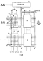
- Fig. 3 illustrates an array of switching matrices 60, 62, 64 and 65.
- Each of these switching matrices comprises the switching network 20 and its associated tri-state buffers 36-46.
- the data lines enter from the left and each line is connected to the respective row of the switching matrix by a tri-state buffer. If lines 66 and 68 are to be interconnected, then cross-points 70 and 72 are turned on as well as the tri-state buffers associated with those rows. All this is performed under the control of the controller 71 linked to the matrices by the control bus 56.
- switching matrix 62 is included. This switching matrix has its own data lines but is connected to the columns 76, 78 and 80 to which the other matrix 60 is connected. If then lines 81 and 82 are to be interconnected, switch points 84 and 86 are turned on as well as their respective row and column tri-state buffers so that column 76 interconnects the two switching matrices 60 and 62, thereby effecting the connection. It is to be noted that the columns on the secondary interconnection array are themselves inactive. At most they have a termination 88 at their ends.
- Additional switching matrices 64 and 65 may also be connected to the same rows on the secondary array as the previously described matrices 60 and 62. These additional arrays may be required to provide full connectivity between the data lines. That is, for a one-sided switch with n lines or n rows, it is required that there be n/2 columns. Only with this number of columns will the system be non-blocking so that there will always be cross-points available if all the lines are being used. However, even if the necessary number of columns are already available, it may be desirable to add additional switching matrices to the rows to provide redundancy and thus fault tolerance to the switching system.
- the switching array 60 fails because of bad cross-points or possibly for other reasons, it may be isolated from the second level of interconnection by its tri-state buffers. In that case an extra array 64 can provide the connectivity that has been lost from the failed switching array 60.
- the degree of duplication of the switching arrays thus depends not only on the size of the switching arrays and the number of lines but also upon the desired data bandwidth (connectivity) and fault tolerance of the system.
- the invention as described above provides a high speed and flexible switch which can be made to be reliable and fault tolerant. It can also be used to implement a large scale switch from smaller, more economical components.
Landscapes
- Engineering & Computer Science (AREA)
- Computer Networks & Wireless Communication (AREA)
- Use Of Switch Circuits For Exchanges And Methods Of Control Of Multiplex Exchanges (AREA)
- Structure Of Telephone Exchanges (AREA)
Applications Claiming Priority (2)
| Application Number | Priority Date | Filing Date | Title |
|---|---|---|---|
| US06/544,652 US4605928A (en) | 1983-10-24 | 1983-10-24 | Fault-tolerant array of cross-point switching matrices |
| US544652 | 1983-10-24 |
Publications (3)
| Publication Number | Publication Date |
|---|---|
| EP0141234A2 true EP0141234A2 (fr) | 1985-05-15 |
| EP0141234A3 EP0141234A3 (en) | 1988-03-23 |
| EP0141234B1 EP0141234B1 (fr) | 1990-12-19 |
Family
ID=24173036
Family Applications (1)
| Application Number | Title | Priority Date | Filing Date |
|---|---|---|---|
| EP84111284A Expired EP0141234B1 (fr) | 1983-10-24 | 1984-09-21 | Réseau de commutation |
Country Status (6)
| Country | Link |
|---|---|
| US (1) | US4605928A (fr) |
| EP (1) | EP0141234B1 (fr) |
| JP (1) | JPH0669232B2 (fr) |
| BR (1) | BR8405375A (fr) |
| CA (1) | CA1225729A (fr) |
| DE (1) | DE3483775D1 (fr) |
Cited By (2)
| Publication number | Priority date | Publication date | Assignee | Title |
|---|---|---|---|---|
| EP0261352A3 (en) * | 1986-09-22 | 1988-10-19 | International Business Machines Corporation | Cross point switch architecture for a micro-pbx |
| WO1997002710A1 (fr) * | 1995-07-05 | 1997-01-23 | Power X Limited | Commutateur de points de connexion de circuits integres |
Families Citing this family (50)
| Publication number | Priority date | Publication date | Assignee | Title |
|---|---|---|---|---|
| US4763122A (en) * | 1987-03-18 | 1988-08-09 | International Business Machines Corporation | Parallel switching with round robin priority |
| DE3802579A1 (de) * | 1988-01-29 | 1989-08-10 | Ant Nachrichtentech | Dreistufiges blockierungsfreies koppelfeld |
| JPH03504663A (ja) * | 1988-03-03 | 1991-10-09 | ジーメンス アクチエンゲゼルシヤフト | 通信伝送装置の作動状態監視装置 |
| US4964105A (en) * | 1988-11-01 | 1990-10-16 | Dsc Communications Corporation | Replacement switch |
| US4929940A (en) * | 1988-11-18 | 1990-05-29 | International Business Machines Corporation | Collision crossbar switch |
| EP0381645A3 (fr) | 1989-01-18 | 1992-08-05 | International Business Machines Corporation | Système et méthode de communication entre plusieurs processeurs |
| US4984237A (en) * | 1989-06-29 | 1991-01-08 | International Business Machines Corporation | Multistage network with distributed pipelined control |
| US5107489A (en) * | 1989-10-30 | 1992-04-21 | Brown Paul J | Switch and its protocol for making dynamic connections |
| US5206860A (en) * | 1990-08-31 | 1993-04-27 | International Business Machines Corporation | Recovery from a possible switching error in a computer i/o system |
| JPH0756644B2 (ja) * | 1990-08-31 | 1995-06-14 | インターナショナル・ビジネス・マシーンズ・コーポレイション | 状態変化通知装置及び方法 |
| US5144293A (en) * | 1990-12-18 | 1992-09-01 | International Business Machines Corporation | Serial link communication system with cascaded switches |
| US5301284A (en) * | 1991-01-16 | 1994-04-05 | Walker-Estes Corporation | Mixed-resolution, N-dimensional object space method and apparatus |
| US5280607A (en) * | 1991-06-28 | 1994-01-18 | International Business Machines Corporation | Method and apparatus for tolerating faults in mesh architectures |
| US5235592A (en) * | 1991-08-13 | 1993-08-10 | International Business Machines Corporation | Dynamic switch protocols on a shared medium network |
| US5576554A (en) * | 1991-11-05 | 1996-11-19 | Monolithic System Technology, Inc. | Wafer-scale integrated circuit interconnect structure architecture |
| US5498990A (en) * | 1991-11-05 | 1996-03-12 | Monolithic System Technology, Inc. | Reduced CMOS-swing clamping circuit for bus lines |
| DE69226150T2 (de) * | 1991-11-05 | 1999-02-18 | Hsu Fu Chieh | Redundanzarchitektur für Schaltungsmodul |
| US5831467A (en) * | 1991-11-05 | 1998-11-03 | Monolithic System Technology, Inc. | Termination circuit with power-down mode for use in circuit module architecture |
| US5450073A (en) * | 1991-12-31 | 1995-09-12 | International Business Machines Corporation | Controlling power sequencing of a control unit in an input/output system |
| US5271014A (en) * | 1992-05-04 | 1993-12-14 | International Business Machines Corporation | Method and apparatus for a fault-tolerant mesh with spare nodes |
| WO1994003901A1 (fr) | 1992-08-10 | 1994-02-17 | Monolithic System Technology, Inc. | Systeme de bus a grande vitesse et interface de bus insensibles aux defaillances pour integration a l'echelle d'une tranche |
| US5349248A (en) * | 1992-09-03 | 1994-09-20 | Xilinx, Inc. | Adaptive programming method for antifuse technology |
| US5513313A (en) * | 1993-01-19 | 1996-04-30 | International Business Machines Corporation | Method for generating hierarchical fault-tolerant mesh architectures |
| US5365512A (en) * | 1993-07-02 | 1994-11-15 | Ericsson Ge Mobile Communications Inc. | Multisite trunked RF communication system with reliable control messaging network |
| US5371786A (en) * | 1993-09-29 | 1994-12-06 | At&T Bell Corp. | Electronic cross-connect system |
| US5655113A (en) | 1994-07-05 | 1997-08-05 | Monolithic System Technology, Inc. | Resynchronization circuit for a memory system and method of operating same |
| JP2886093B2 (ja) * | 1994-07-28 | 1999-04-26 | 株式会社日立製作所 | 障害処理方法および情報処理システム |
| US5812556A (en) * | 1996-07-03 | 1998-09-22 | General Signal Corporation | Fault tolerant switch fabric with control and data correction by hamming codes and error inducing check register |
| US5805614A (en) * | 1996-07-03 | 1998-09-08 | General Signal Corporation | Fault tolerant switch fabric with control and data correction by hamming codes |
| US6377575B1 (en) | 1998-08-05 | 2002-04-23 | Vitesse Semiconductor Corporation | High speed cross point switch routing circuit with word-synchronous serial back plane |
| US6138185A (en) * | 1998-10-29 | 2000-10-24 | Mcdata Corporation | High performance crossbar switch |
| US6346744B1 (en) * | 1999-09-14 | 2002-02-12 | Sarnoff Corporation | Integrated RF M×N switch matrix |
| EP1307820B1 (fr) | 2000-06-06 | 2014-07-23 | Vitesse Semiconductor Corporation | Dispositif de commutation par points de connexion avec module de matrice de commutation |
| US6807269B1 (en) | 2000-07-20 | 2004-10-19 | Cisco Technology, Inc. | Call management implemented using call routing engine |
| US6614904B1 (en) * | 2000-08-09 | 2003-09-02 | Alcatel | Apparatus and method for effecting a communication arrangement between switch arrays |
| US6674852B1 (en) | 2000-08-31 | 2004-01-06 | Cisco Technology, Inc. | Call management implemented using call routing engine |
| US6801613B1 (en) * | 2000-08-31 | 2004-10-05 | Cisco Technology, Inc. | Associating call appearance with data associated with call |
| US6690789B1 (en) * | 2000-08-31 | 2004-02-10 | Cisco Technology, Inc. | Fault tolerant telephony control |
| SE0301439L (sv) * | 2003-05-19 | 2004-11-20 | Nordia Innovation Ab | Anordning för uppbyggnad av väljarmatris med redundans och ingångsorienterad fuktionalitet |
| US7684265B2 (en) * | 2007-02-27 | 2010-03-23 | Analog Devices, Inc. | Redundant cross point switching system and method |
| US12276420B2 (en) | 2016-02-03 | 2025-04-15 | Strong Force Iot Portfolio 2016, Llc | Industrial internet of things smart heating systems and methods that produce and use hydrogen fuel |
| US11774944B2 (en) | 2016-05-09 | 2023-10-03 | Strong Force Iot Portfolio 2016, Llc | Methods and systems for the industrial internet of things |
| US11327475B2 (en) | 2016-05-09 | 2022-05-10 | Strong Force Iot Portfolio 2016, Llc | Methods and systems for intelligent collection and analysis of vehicle data |
| KR102255270B1 (ko) | 2016-05-09 | 2021-05-25 | 스트롱 포스 아이오티 포트폴리오 2016, 엘엘씨 | 산업용 사물 인터넷을 위한 방법들 및 시스템들 |
| US10754334B2 (en) | 2016-05-09 | 2020-08-25 | Strong Force Iot Portfolio 2016, Llc | Methods and systems for industrial internet of things data collection for process adjustment in an upstream oil and gas environment |
| US10983507B2 (en) | 2016-05-09 | 2021-04-20 | Strong Force Iot Portfolio 2016, Llc | Method for data collection and frequency analysis with self-organization functionality |
| US20200133254A1 (en) | 2018-05-07 | 2020-04-30 | Strong Force Iot Portfolio 2016, Llc | Methods and systems for data collection, learning, and streaming of machine signals for part identification and operating characteristics determination using the industrial internet of things |
| KR102061274B1 (ko) * | 2018-08-08 | 2019-12-31 | 재단법인대구경북과학기술원 | 버스네트워크시스템 |
| EP3909223B1 (fr) | 2019-01-13 | 2024-08-21 | Strong Force Iot Portfolio 2016, LLC | Surveiller et gérer des réglages industriels |
| CN112895922B (zh) * | 2021-01-07 | 2022-12-13 | 株洲中车时代电气股份有限公司 | 氢燃料备用电源的监控装置和轨道交通氢燃料列车 |
Family Cites Families (14)
| Publication number | Priority date | Publication date | Assignee | Title |
|---|---|---|---|---|
| NL284363A (fr) * | 1960-03-23 | 1900-01-01 | ||
| DE2251444C2 (de) * | 1972-10-20 | 1983-07-14 | Licentia Patent-Verwaltungs-Gmbh, 6000 Frankfurt | Koppelfeld-Anordnung zur breitbandigen Signalübertragung in Fernmeldeanlagen |
| US3872439A (en) * | 1973-02-09 | 1975-03-18 | Hassan Paddy Abdel Salam | Electronic switching circuit for bidirectional transfer |
| DE2534759B2 (de) * | 1975-08-04 | 1979-07-12 | Siemens Ag, 1000 Berlin Und 8000 Muenchen | Kreuzschienenverteiler |
| IT1071840B (it) * | 1976-11-12 | 1985-04-10 | Olivetti & Co Spa | Sistema multiprocessore per la commutazione automatica di linee telegrafiche e metodo di trasferimento dei caratteri di informazione |
| FR2396484A1 (fr) * | 1977-06-30 | 1979-01-26 | Telic | Matrice de commutation a thyristors |
| US4162535A (en) * | 1977-08-12 | 1979-07-24 | Honeywell Inc. | Triangular high speed I/O system for content addressable memories |
| US4146749A (en) * | 1977-09-16 | 1979-03-27 | Wescom Switching, Inc. | Telecommunications network having multi-function spare network block |
| AU521265B2 (en) * | 1979-08-20 | 1982-03-25 | Nippon Telegraph & Telephone Corporation | Key telephone system |
| DE3165314D1 (en) * | 1980-04-14 | 1984-09-13 | Grundig Emv | Multi-stage coupling field |
| US4331956A (en) * | 1980-09-29 | 1982-05-25 | Lovelace Alan M Administrator | Control means for a solid state crossbar switch |
| US4393381A (en) * | 1981-01-02 | 1983-07-12 | T-Bar Incorporated | Transfer bus matrix |
| US4345251A (en) * | 1981-02-20 | 1982-08-17 | The United States Of America As Represented By The Secretary Of The Navy | Solid state commutator switch |
| US4417245A (en) * | 1981-09-02 | 1983-11-22 | International Business Machines Corp. | Digital space division exchange |
-
1983
- 1983-10-24 US US06/544,652 patent/US4605928A/en not_active Expired - Fee Related
-
1984
- 1984-08-09 CA CA000460687A patent/CA1225729A/fr not_active Expired
- 1984-09-17 JP JP59192753A patent/JPH0669232B2/ja not_active Expired - Lifetime
- 1984-09-21 DE DE8484111284T patent/DE3483775D1/de not_active Expired - Lifetime
- 1984-09-21 EP EP84111284A patent/EP0141234B1/fr not_active Expired
- 1984-10-23 BR BR8405375A patent/BR8405375A/pt not_active IP Right Cessation
Cited By (3)
| Publication number | Priority date | Publication date | Assignee | Title |
|---|---|---|---|---|
| EP0261352A3 (en) * | 1986-09-22 | 1988-10-19 | International Business Machines Corporation | Cross point switch architecture for a micro-pbx |
| US4803720A (en) * | 1986-09-22 | 1989-02-07 | International Business Machines Corporation | Dual plane cross point switch architecture for a micro-PBX |
| WO1997002710A1 (fr) * | 1995-07-05 | 1997-01-23 | Power X Limited | Commutateur de points de connexion de circuits integres |
Also Published As
| Publication number | Publication date |
|---|---|
| EP0141234A3 (en) | 1988-03-23 |
| US4605928A (en) | 1986-08-12 |
| JPS6098790A (ja) | 1985-06-01 |
| DE3483775D1 (de) | 1991-01-31 |
| EP0141234B1 (fr) | 1990-12-19 |
| BR8405375A (pt) | 1985-09-03 |
| JPH0669232B2 (ja) | 1994-08-31 |
| CA1225729A (fr) | 1987-08-18 |
Similar Documents
| Publication | Publication Date | Title |
|---|---|---|
| US4605928A (en) | Fault-tolerant array of cross-point switching matrices | |
| EP0425807B1 (fr) | Commutateur de croisement à rebroussement avec commande distribuée | |
| EP0360540B1 (fr) | Circuit de logique programmable | |
| US5509128A (en) | FPGA architecture including direct logic function circuit to I/O interconnections | |
| US3805039A (en) | High reliability system employing subelement redundancy | |
| CA1245305A (fr) | Commutateur de croisement duplex | |
| US4983961A (en) | Three stage non-blocking switching array | |
| JPH0156595B2 (fr) | ||
| US4354217A (en) | Automatic power disconnect system for wafer scale integrated circuits | |
| GB2188813A (en) | Switching network | |
| US4329685A (en) | Controlled selective disconnect system for wafer scale integrated circuits | |
| CN113114220B (zh) | 一种具有重映射功能的芯片系统及芯片重映射配置系统 | |
| US3937936A (en) | Equipment self-repair by adaptive multifunction modules | |
| EP0299677B1 (fr) | Ensemble de circuits de redondance | |
| US6087958A (en) | Multi-stage routing switchers with sequential and non-repetitive distributive circuit interconnections | |
| JPS582513B2 (ja) | ネットワ−ク駆動方式 | |
| US5189320A (en) | Programmable logic device with multiple shared logic arrays | |
| EP0240805B1 (fr) | Matrice de commutation à commande de courant | |
| US7473851B2 (en) | Cross-connecting by permutations using configurable printed circuits | |
| EP0739146A2 (fr) | Commutateur de télécommunication | |
| KR19990064109A (ko) | 통신시스템에 관한 장치 및 방법 | |
| EP0515043A2 (fr) | Interconnexions directes pour réseau de modules à circuits fonctionnels | |
| SU1309033A1 (ru) | Однородна коммутирующа сеть | |
| SU877548A1 (ru) | Устройство дл управлени переключением резерва | |
| US20080187130A1 (en) | Cross-Connect Arrangement and Switch Matrix |
Legal Events
| Date | Code | Title | Description |
|---|---|---|---|
| PUAI | Public reference made under article 153(3) epc to a published international application that has entered the european phase |
Free format text: ORIGINAL CODE: 0009012 |
|
| 17P | Request for examination filed |
Effective date: 19841123 |
|
| AK | Designated contracting states |
Designated state(s): DE FR GB IT |
|
| PUAL | Search report despatched |
Free format text: ORIGINAL CODE: 0009013 |
|
| AK | Designated contracting states |
Kind code of ref document: A3 Designated state(s): DE FR GB IT |
|
| 17Q | First examination report despatched |
Effective date: 19890824 |
|
| GRAA | (expected) grant |
Free format text: ORIGINAL CODE: 0009210 |
|
| AK | Designated contracting states |
Kind code of ref document: B1 Designated state(s): DE FR GB IT |
|
| REF | Corresponds to: |
Ref document number: 3483775 Country of ref document: DE Date of ref document: 19910131 |
|
| ET | Fr: translation filed | ||
| ITF | It: translation for a ep patent filed | ||
| ITTA | It: last paid annual fee | ||
| PLBE | No opposition filed within time limit |
Free format text: ORIGINAL CODE: 0009261 |
|
| STAA | Information on the status of an ep patent application or granted ep patent |
Free format text: STATUS: NO OPPOSITION FILED WITHIN TIME LIMIT |
|
| 26N | No opposition filed | ||
| PGFP | Annual fee paid to national office [announced via postgrant information from national office to epo] |
Ref country code: FR Payment date: 19950911 Year of fee payment: 12 |
|
| PGFP | Annual fee paid to national office [announced via postgrant information from national office to epo] |
Ref country code: GB Payment date: 19960827 Year of fee payment: 13 |
|
| PGFP | Annual fee paid to national office [announced via postgrant information from national office to epo] |
Ref country code: DE Payment date: 19960917 Year of fee payment: 13 |
|
| PG25 | Lapsed in a contracting state [announced via postgrant information from national office to epo] |
Ref country code: FR Effective date: 19960930 |
|
| REG | Reference to a national code |
Ref country code: FR Ref legal event code: ST |
|
| REG | Reference to a national code |
Ref country code: FR Ref legal event code: ST |
|
| PG25 | Lapsed in a contracting state [announced via postgrant information from national office to epo] |
Ref country code: GB Free format text: LAPSE BECAUSE OF NON-PAYMENT OF DUE FEES Effective date: 19970921 |
|
| GBPC | Gb: european patent ceased through non-payment of renewal fee |
Effective date: 19970921 |
|
| PG25 | Lapsed in a contracting state [announced via postgrant information from national office to epo] |
Ref country code: DE Free format text: LAPSE BECAUSE OF NON-PAYMENT OF DUE FEES Effective date: 19980603 |