EP0141332A2 - Dispositif à plusieurs buses pour la connexion de processeurs et de mémoires dans un système multiprocesseur - Google Patents
Dispositif à plusieurs buses pour la connexion de processeurs et de mémoires dans un système multiprocesseur Download PDFInfo
- Publication number
- EP0141332A2 EP0141332A2 EP84112409A EP84112409A EP0141332A2 EP 0141332 A2 EP0141332 A2 EP 0141332A2 EP 84112409 A EP84112409 A EP 84112409A EP 84112409 A EP84112409 A EP 84112409A EP 0141332 A2 EP0141332 A2 EP 0141332A2
- Authority
- EP
- European Patent Office
- Prior art keywords
- bus
- memory
- coupler
- processor
- buses
- Prior art date
- Legal status (The legal status is an assumption and is not a legal conclusion. Google has not performed a legal analysis and makes no representation as to the accuracy of the status listed.)
- Withdrawn
Links
Images


Classifications
-
- G—PHYSICS
- G06—COMPUTING OR CALCULATING; COUNTING
- G06F—ELECTRIC DIGITAL DATA PROCESSING
- G06F13/00—Interconnection of, or transfer of information or other signals between, memories, input/output devices or central processing units
- G06F13/38—Information transfer, e.g. on bus
- G06F13/40—Bus structure
- G06F13/4004—Coupling between buses
- G06F13/4022—Coupling between buses using switching circuits, e.g. switching matrix, connection or expansion network
-
- G—PHYSICS
- G06—COMPUTING OR CALCULATING; COUNTING
- G06F—ELECTRIC DIGITAL DATA PROCESSING
- G06F13/00—Interconnection of, or transfer of information or other signals between, memories, input/output devices or central processing units
- G06F13/14—Handling requests for interconnection or transfer
- G06F13/16—Handling requests for interconnection or transfer for access to memory bus
- G06F13/1605—Handling requests for interconnection or transfer for access to memory bus based on arbitration
- G06F13/1652—Handling requests for interconnection or transfer for access to memory bus based on arbitration in a multiprocessor architecture
-
- G—PHYSICS
- G06—COMPUTING OR CALCULATING; COUNTING
- G06F—ELECTRIC DIGITAL DATA PROCESSING
- G06F13/00—Interconnection of, or transfer of information or other signals between, memories, input/output devices or central processing units
- G06F13/14—Handling requests for interconnection or transfer
- G06F13/36—Handling requests for interconnection or transfer for access to common bus or bus system
-
- G—PHYSICS
- G06—COMPUTING OR CALCULATING; COUNTING
- G06F—ELECTRIC DIGITAL DATA PROCESSING
- G06F15/00—Digital computers in general; Data processing equipment in general
- G06F15/16—Combinations of two or more digital computers each having at least an arithmetic unit, a program unit and a register, e.g. for a simultaneous processing of several programs
- G06F15/163—Interprocessor communication
- G06F15/173—Interprocessor communication using an interconnection network, e.g. matrix, shuffle, pyramid, star, snowflake
Definitions
- the invention relates to a multiple bus arrangement for the connection of processors and memories in a multiprocessor system, in which each processor is connected to at least one bus by a processor connection bus via a respective coupler and the memory is connected to at least one bus by a memory connection bus via a respective coupler is.
- each processor can be connected to every bus and each memory to each bus via a coupler. This increases the safety and availability of the multiprocessor system, however, at the expense of great effort, since a large number of couplers and controls are required for the couplers.
- the object on which the invention is based is to design the multiple bus arrangement for the connection of processors and memories in a multiple processor system in such a way that the throughput of data is as high as possible and nevertheless the outlay on hardware is as low as possible.
- This object is achieved in a multiple bus arrangement of the type specified in the introduction in that each processor is connected to each bus by a coupler and in that each memory is connected to only a part of the buses via a coupler.
- each processor is only connected to a part of the buses via a coupler and that each memory can be connected to each bus by a coupler.
- each memory is only connected to one bus via a coupler, the savings on couplers per memory are greatest. However, this has the disadvantage that no fault tolerance is possible. Falls e.g. the coupler assigned to the memory, then this memory can no longer be accessed. In order to make the multiple bus arrangement redundant in this case, it is advantageous that each memory is connected to at least two buses via a coupler.
- a processor can be connected to more than one bus via a coupler and can be achieved in that a fault tolerance is possible.
- the efficiency of the multiple bus arrangement is further increased by the fact that at least one bus is provided for block transfers or for an uninterruptible sequence of accesses by a processor. This bus then only connects the memories and processors that can work in such an operating mode.
- a multiple bus arrangement for a multiprocessor system for example from the literature cited above place is known.
- a plurality of buses B 1 ... B i are provided here, to which processors P and memory S are connected via couplers K.
- the processors P 1 ... P n can each be connected via processor connection buses PB 1 ... PB n to all buses B 1 ... B i via couplers KP.
- all memories S 1 ... S m can each be connected via memory connection buses SB 1 ... SB m to all buses B 1 ... B i via couplers KS.
- the disadvantage of such a multiple bus arrangement is that a large number of couplers KP or KS is required.
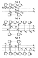
- the number of couplers in the multiple bus arrangement is reduced if the memory-dependent bus selection method is selected according to FIG. 2.
- Fig. 2 only three buses B 1 , B 2 and B 3 are shown.
- the processors P 1 ... P n are connected to the buses B 1 ... B 3 in accordance with FIG. 1. That is, each processor P 1 ... P n is connected to each bus B 1 ... B 3 connected.
- the connection of the memories S to the buses B 1 ... B 3 is different from FIG.
- the memory S 1 is only with the bus B n via the coupler KS 1,1
- the memory S 2 only with the bus B 2 via the coupler KS 2,2
- the memory S 3 only with the bus B 3 the coupler KS 3.3 can be connected .
- bus-dependent bus selection method can be implemented simply by using a log 2 (S) bit-wide binary word as the memory address and any bits therefrom, for example the most significant bits removed and used as bus address.
- each memory S 1 ... S m is connected to each bus via a coupler KS.
- each processor P is only connected to one bus via a coupler KP.
- the processor P1 is required for each processor P, and the number of couplers per processor is considerably lower than in the embodiment of FIG. 1.
- the processor P1 is only connected to only the bus B l, and said processor P 3 and P 4 with the bus B2.
- the choice of the bus used for the access depends on which processor carries out the access. If, therefore, will perform an access such as the processor P 1, he must use the bus B, to bring about the coupling by the coupler KP 1.1 to the bus B 1 and may then each store S 1 ... S m via the couplers KS head for.
- the efficiency of a multiple bus arrangement can be stored in that, according to FIG. 4, the processors are divided into classes with different access privileges. Then each bus is assigned a number of processors which is dependent on the class division, so that in each case many processors with low access privileges share a bus, but only a few processors with high access privilege are each connected to a bus.
- the processor P 1 has the highest access privilege and is only connected to a bus B 1 .
- Two processors with the next lowest access privilege, in Fig. 4 with P P , P 3 . are connected to a second bus B 2 together .
- three processors P 4 , P 5 , P 6 with the lowest access privilege are connected to the bus B 3 .
- the memories S 1 ... S m can be connected to all buses B 1 ... B 3 via couplers KS.
- the efficiency of a multiple bus arrangement can also be increased by classifying the memories with different access times according to access times. Then a bus is assigned to a few fast memories or many slow memories. 5, for example, the memory S 1 has the shortest access time and is only connectable to a bus B 1 via the coupler KS 1 .
- the two memories S 2 , S 3 have a higher access time than the memory S 1 and can be connected together to the bus B 2 via the coupler KS 2 .
- the three stores. S 4 , S 5 , S 6 finally have the highest access time and are connected together to bus B 3 via coupler KS 3 .
- the processors P 1 ... P n can each be connected to all buses B 1 ... B 3 via couplers KP.
- FIGS. 2 to 5 have the disadvantage that if a coupler or a bus fails, the assigned connection path is interrupted and this connection path can therefore no longer be used for access. Since there is no other connection path, the processor can no longer access the memory between which the interrupted connection path lies.
- the multiple bus arrangement according to FIG. 6 can be designed such that, for example, each processor P can be connected to two buses B 1 and B 2 via couplers KP. 6 shows the processor-dependent bus selection method in which the memories S 1 ... S 3 are each connected to all buses B 1 ... B 3 .
- processor P 1 for example, is to access memory S 1 and, for example, coupler KP 1 fails and thus the connection path via bus B 1 , then there is still the connection path via B 2 , coupler KP 2 to the memory S 1 .
- the failure of a coupler or a bus does not prevent access to a memory S.
- a multiple bus arrangement can also be constructed for a memory-dependent bus selection method. Then each processor P can be connected to each bus via a coupler, whereas each memory S can be connected to two buses. If a coupler or a bus fails, then access from a processor to this memory is still possible via the other coupler and the other bus.
- the coupler K has two tristate drivers TS 1 , TS 2 , via which the processor connection bus PB, as in FIG. 7, or a memory connection bus can be connected to the bus B. Furthermore, an address recognition logic AEL is provided, which recognizes which memory is to be accessed via which bus. The corresponding address is fed to the address recognition logic via the processor connection bus PB. If the processor P issues an address assigned to the bus B, the address recognition logic AEL issues a signal REQ which is fed to an arbiter ARB. The arbiter ARB checks whether there are requests for access from other processors. For this purpose, it is connected via lines L 1 , L 2 , L 3 to the arbiters assigned to the other processors.
- the arbiter ARB emits a signal ACK which drives one of the tristate drivers TS.
- the tristate driver TS 1 or the tristate driver TS 2 is controlled.
- the building blocks used in FIG. 7 are known building blocks.
- a 74241 module can be used as the tri-state driver and an Intel arbitration chip 8289 can be used as the arbiter ARB.
- the address recognition logic AEL can be constructed as a comparator.
- processors P ie processors P, memory S or buses B, are likewise of a known design.
Landscapes
- Engineering & Computer Science (AREA)
- Theoretical Computer Science (AREA)
- Physics & Mathematics (AREA)
- General Engineering & Computer Science (AREA)
- General Physics & Mathematics (AREA)
- Computer Hardware Design (AREA)
- Mathematical Physics (AREA)
- Software Systems (AREA)
- Multi Processors (AREA)
Applications Claiming Priority (2)
| Application Number | Priority Date | Filing Date | Title |
|---|---|---|---|
| DE3338341 | 1983-10-21 | ||
| DE19833338341 DE3338341A1 (de) | 1983-10-21 | 1983-10-21 | Mehrfachbusanordnung fuer die verbindung von prozessoren und speichern in einem mehrprozessorsystem |
Publications (2)
| Publication Number | Publication Date |
|---|---|
| EP0141332A2 true EP0141332A2 (fr) | 1985-05-15 |
| EP0141332A3 EP0141332A3 (fr) | 1986-09-10 |
Family
ID=6212458
Family Applications (1)
| Application Number | Title | Priority Date | Filing Date |
|---|---|---|---|
| EP84112409A Withdrawn EP0141332A3 (fr) | 1983-10-21 | 1984-10-15 | Dispositif à plusieurs buses pour la connexion de processeurs et de mémoires dans un système multiprocesseur |
Country Status (2)
| Country | Link |
|---|---|
| EP (1) | EP0141332A3 (fr) |
| DE (1) | DE3338341A1 (fr) |
Cited By (7)
| Publication number | Priority date | Publication date | Assignee | Title |
|---|---|---|---|---|
| EP0458516A3 (en) * | 1990-05-25 | 1992-04-08 | American Telephone And Telegraph Company | Memory access bus arrangement |
| EP0335968B1 (fr) * | 1987-10-16 | 1993-08-04 | Digital Equipment Corporation | Coupleur d'interconnexion d'ordinateur utilisant une commutation a barres croisees |
| EP0494056A3 (en) * | 1990-12-31 | 1994-08-10 | Ibm | Dynamically partitionable and allocable bus structure |
| WO1996030842A1 (fr) * | 1995-03-27 | 1996-10-03 | International Business Machines Corporation | Structure de bus pour un systeme multiprocesseur |
| GB2332344A (en) * | 1997-12-09 | 1999-06-16 | Sony Uk Ltd | Set top box integrated circuit |
| WO2000043894A3 (fr) * | 1999-01-21 | 2001-02-08 | Analog Devices Inc | Procede et dispositif permettant la communication entre plusieurs unites fonctionnelles dans un environnement informatique |
| WO2001009741A3 (fr) * | 1999-07-30 | 2001-08-30 | Siemens Ag | Systeme multiprocesseur pour l'execution d'acces a une memoire commune ainsi que procede correspondant |
Families Citing this family (3)
| Publication number | Priority date | Publication date | Assignee | Title |
|---|---|---|---|---|
| FI84114C (fi) * | 1988-02-17 | 1991-10-10 | Valtion Teknillinen | Inkopplingssystem. |
| DE4143584C2 (de) * | 1990-06-04 | 2002-10-10 | Hitachi Ltd | Informationsverarbeitungssystem |
| DE19841183C2 (de) * | 1998-09-09 | 2000-08-10 | Daimler Chrysler Ag | Vorrichtung zur Kopplung von redundanten elektronischen Schaltungen über redunante Busse ohne Fehlerfortpflanzung |
Family Cites Families (1)
| Publication number | Priority date | Publication date | Assignee | Title |
|---|---|---|---|---|
| GB1394431A (en) * | 1971-06-24 | 1975-05-14 | Plessey Co Ltd | Multiprocessor data processing system |
-
1983
- 1983-10-21 DE DE19833338341 patent/DE3338341A1/de not_active Withdrawn
-
1984
- 1984-10-15 EP EP84112409A patent/EP0141332A3/fr not_active Withdrawn
Cited By (10)
| Publication number | Priority date | Publication date | Assignee | Title |
|---|---|---|---|---|
| EP0335968B1 (fr) * | 1987-10-16 | 1993-08-04 | Digital Equipment Corporation | Coupleur d'interconnexion d'ordinateur utilisant une commutation a barres croisees |
| EP0458516A3 (en) * | 1990-05-25 | 1992-04-08 | American Telephone And Telegraph Company | Memory access bus arrangement |
| EP0494056A3 (en) * | 1990-12-31 | 1994-08-10 | Ibm | Dynamically partitionable and allocable bus structure |
| WO1996030842A1 (fr) * | 1995-03-27 | 1996-10-03 | International Business Machines Corporation | Structure de bus pour un systeme multiprocesseur |
| GB2332344A (en) * | 1997-12-09 | 1999-06-16 | Sony Uk Ltd | Set top box integrated circuit |
| EP0923232A3 (fr) * | 1997-12-09 | 2002-02-13 | Sony United Kingdom Limited | Circuit intégré pour décodeur de télévision |
| WO2000043894A3 (fr) * | 1999-01-21 | 2001-02-08 | Analog Devices Inc | Procede et dispositif permettant la communication entre plusieurs unites fonctionnelles dans un environnement informatique |
| US6618777B1 (en) | 1999-01-21 | 2003-09-09 | Analog Devices, Inc. | Method and apparatus for communicating between multiple functional units in a computer environment |
| CN1315069C (zh) * | 1999-01-21 | 2007-05-09 | 模拟装置公司 | 在计算机环境中用于多重功能单元之间通信的方法和装置 |
| WO2001009741A3 (fr) * | 1999-07-30 | 2001-08-30 | Siemens Ag | Systeme multiprocesseur pour l'execution d'acces a une memoire commune ainsi que procede correspondant |
Also Published As
| Publication number | Publication date |
|---|---|
| EP0141332A3 (fr) | 1986-09-10 |
| DE3338341A1 (de) | 1985-05-09 |
Similar Documents
| Publication | Publication Date | Title |
|---|---|---|
| DE3938018C3 (de) | Informationsverarbeitungssystem und Verfahren zur Bestimmung von dessen Konfiguration | |
| DE3909948C2 (fr) | ||
| DE69915243T2 (de) | Speicherplattenanordnung-Steuerungsvorrichtung | |
| DE2717503C2 (de) | Mehrprozessor-Mikrorechnersystem | |
| DE2829550C2 (fr) | ||
| DE69736872T2 (de) | Datenverarbeitungssystem | |
| DE3146356A1 (de) | Datenverarbeitungssystem | |
| DE2313724A1 (de) | Elektronische datenverarbeitungsanlage | |
| DE3224034A1 (de) | Mehrprozessorensystem | |
| DE3049774C2 (fr) | ||
| DE2523372B2 (de) | Eingabe-ZAusgabe-Anschlußsteuereinrichtung | |
| DE4135830A1 (de) | Parallelinterface | |
| EP0141332A2 (fr) | Dispositif à plusieurs buses pour la connexion de processeurs et de mémoires dans un système multiprocesseur | |
| EP0062141B1 (fr) | Circuit pour l'entrée de signaux de commande d'exécution dans un système de micro-ordinateur | |
| DE69131417T2 (de) | Bussystem | |
| DE69429325T2 (de) | Datenvermittlungsvorrichtung | |
| DE3009530C2 (fr) | ||
| DE29521444U1 (de) | Anordnung mit Master- und Slave-Einheiten | |
| DE3142504A1 (de) | Mehrfachplattenspeicher-uebertragungssystem | |
| DE2142374C2 (de) | Schaltungsanordnung zur Auswahl und ggfs. erfolgenden Modifizierung von Datenzeichen | |
| WO1994012936A1 (fr) | Dispositif pour la transmission de donnees au moyen d'un bus | |
| DE69312174T2 (de) | Gerät zur Verwaltung von Zugriffspriorität zu gemeinsamen Betriebsmitteln von unter einer Vielzahl von lokalen Einheiten verteilten Funktionsmodulen, von denen jede eine lokale "Daisy-Chain"-Schaltung formt | |
| DE3247083A1 (de) | Mehrprozessorsystem | |
| DE3780526T2 (de) | Synchronisationsvorrichtung fuer die interrupt-ebene-aenderung multiprocessoren. | |
| DE69421334T2 (de) | Verarbeitungssystem mit gemeinschaftlichem Speicher |
Legal Events
| Date | Code | Title | Description |
|---|---|---|---|
| PUAI | Public reference made under article 153(3) epc to a published international application that has entered the european phase |
Free format text: ORIGINAL CODE: 0009012 |
|
| AK | Designated contracting states |
Designated state(s): AT CH DE FR GB IT LI |
|
| RTI1 | Title (correction) | ||
| 17P | Request for examination filed |
Effective date: 19850827 |
|
| PUAL | Search report despatched |
Free format text: ORIGINAL CODE: 0009013 |
|
| AK | Designated contracting states |
Kind code of ref document: A3 Designated state(s): AT CH DE FR GB IT LI |
|
| 17Q | First examination report despatched |
Effective date: 19880719 |
|
| STAA | Information on the status of an ep patent application or granted ep patent |
Free format text: STATUS: THE APPLICATION IS DEEMED TO BE WITHDRAWN |
|
| 18D | Application deemed to be withdrawn |
Effective date: 19890503 |
|
| RIN1 | Information on inventor provided before grant (corrected) |
Inventor name: JEFFRE, THOMAS, DIPL.-INFORM. |