EP0141425B1 - Kleinflächiger Dünnfilmtransistor - Google Patents
Kleinflächiger Dünnfilmtransistor Download PDFInfo
- Publication number
- EP0141425B1 EP0141425B1 EP84113428A EP84113428A EP0141425B1 EP 0141425 B1 EP0141425 B1 EP 0141425B1 EP 84113428 A EP84113428 A EP 84113428A EP 84113428 A EP84113428 A EP 84113428A EP 0141425 B1 EP0141425 B1 EP 0141425B1
- Authority
- EP
- European Patent Office
- Prior art keywords
- layer
- thin film
- drain
- source
- photoresist
- Prior art date
- Legal status (The legal status is an assumption and is not a legal conclusion. Google has not performed a legal analysis and makes no representation as to the accuracy of the status listed.)
- Expired
Links
Images


Classifications
-
- H—ELECTRICITY
- H10—SEMICONDUCTOR DEVICES; ELECTRIC SOLID-STATE DEVICES NOT OTHERWISE PROVIDED FOR
- H10D—INORGANIC ELECTRIC SEMICONDUCTOR DEVICES
- H10D30/00—Field-effect transistors [FET]
- H10D30/01—Manufacture or treatment
- H10D30/021—Manufacture or treatment of FETs having insulated gates [IGFET]
- H10D30/031—Manufacture or treatment of FETs having insulated gates [IGFET] of thin-film transistors [TFT]
- H10D30/0321—Manufacture or treatment of FETs having insulated gates [IGFET] of thin-film transistors [TFT] comprising silicon, e.g. amorphous silicon or polysilicon
-
- H—ELECTRICITY
- H10—SEMICONDUCTOR DEVICES; ELECTRIC SOLID-STATE DEVICES NOT OTHERWISE PROVIDED FOR
- H10D—INORGANIC ELECTRIC SEMICONDUCTOR DEVICES
- H10D30/00—Field-effect transistors [FET]
- H10D30/60—Insulated-gate field-effect transistors [IGFET]
- H10D30/67—Thin-film transistors [TFT]
- H10D30/6728—Vertical TFTs
-
- H—ELECTRICITY
- H10—SEMICONDUCTOR DEVICES; ELECTRIC SOLID-STATE DEVICES NOT OTHERWISE PROVIDED FOR
- H10P—GENERIC PROCESSES OR APPARATUS FOR THE MANUFACTURE OR TREATMENT OF DEVICES COVERED BY CLASS H10
- H10P50/00—Etching of wafers, substrates or parts of devices
- H10P50/69—Etching of wafers, substrates or parts of devices using masks for semiconductor materials
- H10P50/691—Etching of wafers, substrates or parts of devices using masks for semiconductor materials for Group IV materials or Group III-V materials
- H10P50/693—Etching of wafers, substrates or parts of devices using masks for semiconductor materials for Group IV materials or Group III-V materials characterised by their size, orientation, disposition, behaviour or shape, in horizontal or vertical plane
- H10P50/694—Etching of wafers, substrates or parts of devices using masks for semiconductor materials for Group IV materials or Group III-V materials characterised by their size, orientation, disposition, behaviour or shape, in horizontal or vertical plane characterised by their behaviour during the process, e.g. soluble masks or redeposited masks
-
- H—ELECTRICITY
- H10—SEMICONDUCTOR DEVICES; ELECTRIC SOLID-STATE DEVICES NOT OTHERWISE PROVIDED FOR
- H10P—GENERIC PROCESSES OR APPARATUS FOR THE MANUFACTURE OR TREATMENT OF DEVICES COVERED BY CLASS H10
- H10P50/00—Etching of wafers, substrates or parts of devices
- H10P50/69—Etching of wafers, substrates or parts of devices using masks for semiconductor materials
- H10P50/691—Etching of wafers, substrates or parts of devices using masks for semiconductor materials for Group IV materials or Group III-V materials
- H10P50/693—Etching of wafers, substrates or parts of devices using masks for semiconductor materials for Group IV materials or Group III-V materials characterised by their size, orientation, disposition, behaviour or shape, in horizontal or vertical plane
- H10P50/695—Etching of wafers, substrates or parts of devices using masks for semiconductor materials for Group IV materials or Group III-V materials characterised by their size, orientation, disposition, behaviour or shape, in horizontal or vertical plane characterised by the process involved to create the mask, e.g. lift-off masks or sidewalls or to modify the mask
Definitions
- the present invention relates to high performance, thin film field effect transistors which are of small area, which can be operated at high speed, and which provides high output currents, the transistors including a surface, non-coplanar with and angled with respect to a substrate surface, in an etchable layer, which may include sublayers.
- a surface illustrated as surface 20 in the drawings, will henceforth be identified as a non-coplanar surface for ease of reference.
- Thin film field effect transistors generally comprise source and drain electrodes interconnected by a semiconductor material. Conduction between the electrodes takes place primarily within the semiconductor through a current conduction channel between the source and drain electrodes. The current flow between the electrodes is controlled by the application of a voltage to a gate which is adjacent at least a portion of the semiconductor and is insulated therefrom.
- the device output current and operating speed is largely dependent upon the length of the current conduction channel between the source and drain. More particularly, the output current is inversely proportional to the channel length and the operating frequency is inversely proportional to the square of the channel length. Hence, if the channel length of a device can be reduced from 10 ⁇ to 1 ⁇ m, the output current could be increased ten times and the operating speed could be increased one hundred times. In addition, if the channel length could be decreased as above, the width of the device could be decreased. For example, typical planar thin film field effect transistors have a channel length of 10 width of about 500 ⁇ m and provide output current of about 10 microamps.
- the channel length of that device could be reduced to one micron, that same 10 microamps of current could be provided by a - device only 50 um wide.
- the total area of the device could be reduced by a factor of ten and thus the packing density could be increased by a factor of ten.
- the capacitance of the device can also be reduced by a factor of ten.
- the resulting device while providing the same current and occupying one-tenth the area, could also exhibit an operating frequency one hundred times higher than the original thin film field effect transistors having the 10 pm channel.
- the channel length in conventional thin film field effect transistors cannot be readily reduced from the standard channel length of 10 pm to a channel length of 1 um. The reason for this is that the channel length is determined by the spacing between the drain and source electrodes.
- Conventional large area photolithography the process by which the device structures are formed across 30 cm (12 inch) distances, has a feature size of 10 pm. Hence, with conventional photolithography as used for large area, the minimum channel length obtainable is 10 pm.
- the present invention provides a new and improved method of making thin film field effect transistor device structures of the aforementioned type wherein extremely short channel lengths can be provided without the need for precise photolithography. Furthermore, the method of the present invention allows the short channel lengths to be accurately controlled and maintained over large areas.
- the present invention provides a thin film field effect transistor as set out in claim 1 whose precharacterising part corresponds to the disclosure in DE-A-3046358.
- the method of forming the non-coplanar surface in an etchable layer which may include one or more sublayers comprises the steps of depositing a layer of photoresist over the etchable layer, forming a non-coplanar surface in the layer of photoresist, and exposing the etchable layer to an etch through the non-coplanar surface in the photoresist to form the non-coplanar surface in the etchable layer below the non-coplanar surface in the photoresist.
- the etch used is a plasma etch
- the step of forming the non-coplanar surface in the photoresist includes the steps of underexposing and overdeveloping the photoresist. It is preferred that the photoresist be underexposed by at least 20%, and that a patterning mask be placed over the photoresist during the underexposing step. It is also preferred that the step of overdeveloping the photoresist include the use of an active developer solution of enhanced activity, and that the photoresist be a positive photoresist of a thickness of 3 to 3.5 microns.
- the layer of etchable material includes a first conductive layer, an insulating layer deposited over the first conductive layer, and a second conductive layer deposited over the insulating layer.
- a further step comprises depositing a semiconductor layer over at least a portion of the non-coplanar surface formed in the layer of etchable material, so that it forms an electrical connection with the first and second conductive layer.
- the method further includes depositing a gate insulating layer over at least a portion of the semiconductor layer, and depositing a gate electrode layer over at least a portion of the gate insulating layer adjacent to the semiconductor layer.
- the layer of etchable material in which the non-coplanar surface is formed is made of metal.
- this metal layer of etchable material is formed on top of at least one more additional layer of etchable material, and the method includes the further step of using the metal layer of etchable material, once the non-coplanar surface has been formed in it, as a mask during a plasma etching process used to form a non-coplanar surface in the at least one additional layer.
- the metal of the metal layer of etchable material be subject to etching by a first type of etch, but be substantially resistant etching by the type of plasma etch used to form the non-coplanar surface in the at least one additional layer.
- this method of using the metal layer as a mask during plasma etching of layers below it is used in the formation of thin film field effect transistors.
- the metal layer of etchable material and the at least one additional layer of etchable material include between them a first conductive layer, an insulating layer deposited over the first conductive layer, and a second conductive layer deposited over the insulating layer.
- This embodiment includes the further step of depositing a semiconductor layer over at least a portion of the non-coplanar surface formed in the at least one additional layer of etchable material, so as to form an electrical connection with the first and second conductive layers.
- the method further includes depositing a gate insulating layer over at least a portion of the semiconductor layer, and further depositing a gate electrode layer over at least a portion of the gate insulating layer adjacent to the semiconductor layer.
- the first and second layers are formed of metal.
- the present invention relates to high performance, small area, thin film transistors of the general type disclosed and claimed in the above mentioned DE-A-30 46 358.2 for Thin Film Transistor filed in the names of Richard A. Flasck et al., which is incorporated herein by reference, and which is assigned to the assignee of the present invention.
- such thin film transistors have their source and drain regions formed as layers and have a further layer sandwiched between these sources and drain layers. Furthermore they have a surface which is non-coplanar relative to the substrate on which they are formed cut through these layers.
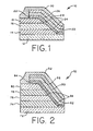
- the transistor 10 is formed on a substrate 12 of insulating material which could be glass, single crystalline silicon, mylar, or an insulator on top of a metal, such as a dielectric overlying a stainless steel surface.
- a substrate 12 of insulating material which could be glass, single crystalline silicon, mylar, or an insulator on top of a metal, such as a dielectric overlying a stainless steel surface.
- Deposited on the substrate 12 is a first layer 14 of conductive drain metal, most commonly a drain layer.
- drain metal layer 14 is a layer 16 of insulating material.
- the insulating material is preferably of a dielectric material.
- the dielectric material can be silicon oxide (SiO,,), silicon nitride (Si x Ny), silioxynitride (SiO X Ny) or aluminum oxide (AI 2 0 3 ).
- a second layer 18 of conductive metal, most commonly a source layer is deposited over the insulative layer 16.
- the source metal 18 and drain metal 14 can be formed of any suitable conductive metal, such as aluminum, molybdenum, or molybdenum tantilum alloy such as (MO. 975 Ta. 025 )-
- layers 14, 16 and 18 have been deposited, all of the layers can be etched in one continuous step, in accordance with the teachings of the present invention, in order to create a non-coplanar surface 20, substantially non-horizontal with respect to the substrate 12 and the stacked layers 14 and 16.
- the non-coplanar or diagonal surface 20 is defined by the exposed edge portions of the source layer 18, the insulative layer 16, and the drain layer 14.
- a non-coplanar surface is meant to be a surface which defines one or more planes which are non-parallel with respect to the substrate although it may include minor plane portions which are parallel to the substrate.
- the semiconductor material is preferably an amorphous silicon alloy including hydrogen, or fluorine, or hydrogen and fluorine.
- the deposited semiconductor material can also be a polycrystalline silicon alloy.
- the semiconductor material 22 is electrically coupled to the source 18 and drain 14 and therefore, a short current conduction channel 24 results in the semiconductor material layer 22 between the source layer 18 and drain layer 14.
- a gate insulator layer 26 of insulating material is then deposited over a portion of the amorphous semiconductor material layer 22.
- the gate insulator is preferably a dielectric such as silicon oxide or silicon nitride.
- the portion of the semiconductor material layer 22 adjacent the source 18 is greater in thickness than the portion forming the current conduction channel 24. This provides some decoupling between the gate and source and therefore improves the high frequency characteristics of the device.
- a gate electrode or conductor 28 which can be made of any suitable metal such as aluminum, molybdenum, chrome or molybdenum tantalum alloy, for example.
- the gate electrode 28 is formed over a portion of the gate insulator 26 and adjacent to the current conduction channel 24.
- a passivating layer 30, such as an oxide or polymer, is formed over the device.
- the source metal 18 and the drain metal 14 can typically have thicknesses ranging from 100 to 300 nm (1,000 to 3,000 A), with the thickness preferably being 250 nm (2,500 A).
- the insulative layer 16 can typically have a thickness between .5 to 3 pm, preferably about 0.8 (3m, and the gate insulator layer 26 can typically have a thickness of between 30 to 500 nm (300 to 5,000 A), and preferably 200 nm (2,000 A).
- the layers of material can be deposited by various deposition techniques, such as sputtering and plasma enhanced chemical vapor deposition.
- the non-coplanar surface 20 can be formed by a dry process that simultaneously etches through the three layers in a continuous one-step process. The process will be explained subsequently in further detail.
- FIG. 2 there is illustrated another thin film, field effect transistor 70 in accordance with the teachings of the present invention.
- a layer of drain metal-74 On an insulating substrate 72 is first deposited a layer of drain metal-74.
- a layer 76 of insulative material On top of the drain metal 74 is deposited a layer 76 of insulative material.
- a layer of source metal 78 On top of the source layer 78 is formed a second layer 80 of insulative material having a thickness from about.5 to 1.5 pm.
- a layer of semiconductor material 84 is formed over the surface 82 and over a portion of second insulative layer 80.
- a short current conduction channel 86 results in the semiconductor material layer 84 between the drain layer 74 and the source layer 78.
- a gate insulator layer 88 is then formed over the semiconductor material layer 84.
- a gate electrode 90 is formed over a portion of the gate insulator layer 88 adjacent to the current conduction channel 86.
- the insulative layer 76 is preferably made of dielectric material such as silicon oxide, silicon nitride, or aluminum oxide.
- the second insulative layer 80 is also of a dielectric material, preferably silicon oxide or silicon nitride.
- the source layer 78 and the drain layer 74 are preferably formed from a metal such as aluminum or molybdenum by sputtering.
- the layer of semiconductor material is deposited on surface 82 by using glow discharge decomposition techniques.
- a top oxide or polymer passivating layer 92 can also be formed over the device.
- the thin film, field effect transistor, and the- various specific embodiments thereof described above provide high performance and small area thin film transistors.
- the top passivating or insulating layer of the transistors such as layers 30 and 92 in Figures 1 and 2, can be utilized to form an insulating layer for another transistor to be formed thereon to provide a stacked transistor configuration to further increase the packing density of the devices.
- Figure 3A illustrates a glass substrate 12 made of 7059 series glass having three layers deposited thereon.
- the layers consist of a drain layer 14 preferably made of molybdenum, an insulative layer 16 preferably made of silicon oxide, and a source layer 18 preferably made of molybdenum.
- the drain and source layers are deposited by sputtering and the insulating layer is deposited by. plasma enhanced chemical vapor deposition.
- the drain and the source layers preferably have thicknesses of 250 nm (2,500 A) and the insulative layer preferably has a thickness of about .8 pm.
- a layer of positive photoresist 100 having a thickness of about 3 to 3.5 pm is deposited over the source layer 18.
- the positive photoresist 100 is deposited by using a spin coating method and the positive photoresist is, for example, Shipley's p-type AZ 1350J.
- a mask 102 is placed over a portion of the positive photoresist layer 100.
- the unmasked portion of layer 100 is then exposed to a collimated light source 104 having an intensity of 300 millijoules/cm 2 for a period of 16 seconds.
- the layer 100 is underexposed and overdeveloped.
- the layer 100 can be underexposed by about 20% since the normal intensity of exposure is 650 millijoules/cm 2 for 16 seconds.
- a negative photoresist could alternatively be used. However, when a negative photoresist is used, the photoresist should be overexposed and underdeveloped. Also, the mask configuration would have to be inverted from that illustrated herein.
- the photoresist layer 100 is actively developed.
- the photoresist can be developed in a developer of enhanced activity, or for a longer time, or for a longer time and in a developer of enhanced activity.
- one part of Shipley developer AZ-311 is used along with three parts water to create an active developer solution. Only the exposed portions of the positive photoresist layer 100 are soluble to the active developer solution. Since the positive photoresist is eroded during this process, the coating thickness of the positive photoresist can be critical. In order to etch a 2 ⁇ m wide channel with a photoresist mask, a 3 to 3.5 p m thick photoresist is preferred.
- a tapered surface 106 results on a portion of layer 100.
- the tapered surface 106 will serve as a mask for the three layers below the positive photoresist layer 100 when the device is subjected to a plasma etching process.
- Figure 3E illustrates the structure that results after plasma etching wherein a non-coplanar surface 20 with respect to the substrate 12 is formed.
- Plasma etching is a process by which gases are used to produce anisotropic etches on various layers of a particular device in order to create a particular profile.
- gases which can be used in the plasma etching include sulfur hexafluoride (SF 6 ), carbon tetrafluoride (CF 4 ) and oxygen (0 2 ).
- SF 6 sulfur hexafluoride
- CF 4 carbon tetrafluoride
- oxygen (0 2 ).
- the flow rates for these gases preferably are: 50 SCCM (standard cubic centimeters per minute) for SF s ; 100 SCCM for CF 4 ; and 10 SCCM for 0 2 .
- the chamber pressure is between 66 and 400 Pa (50 and 300 microns of mercury) and the temperature is preferably close to room temperature (20° to 23°C).
- the radio frequency power is preferably about 1,000 to 2,000 watts having a frequency of 13.56 MHz.
- the electrode size is, for example, 15x 15 cm (6x6 inches) and the electrode spacing can be between 0.48 and 5 cm (3/16 inch and 2 inches). The power density for such a system is therefore between about 10 and 20 watts/cm 2 .
- fluorinated carbon gases are used to etch the composite structure illustrated in Figure 3E.
- CF 3 radicals are the primary etch species for the silicon oxide (Si0 2 ).
- the etching mechanism where the oxide is Si0 2 and the metal is molybdenum is as follows:
- a layer of semiconductor material 120 is formed by plasma assisted chemical vapor deposition, i.e. glow discharge as disclosed, for example, in US-A-4,226,898 which issued on October 7, 1980 in the names of Stanford R. Ovshinsky and Arun Madan for Amorphous Semiconductors Equivalent to Crystalline Semiconductors Produced by a Glow Discharge Process, over the non-coplanar surface 20 and the source layer 18.
- the purpose of the following steps is to form the semiconductor layer 120 so that it covers the non-coplanar surface 20 and a portion of the source layer 18 of the device.
- a negative photoresist layer 122 is formed over the amorphous semiconductor material layer 120.
- a mask 124 is then placed over a portion of the negative photoresist layer 122.
- a light source 126 illuminates the exposed portions of the negative photoresist layer 122.
- the photoresist layer 122 is exposed, for example, by using a light having an intensity of 300 millijoules/cm 2. Due to the use of a negative photoresist, the exposed portions harden and become insoluble to an active developer solution. The unexposed portions are soluble to that particular solution.
- Figure 3G illustrates the removed portion 128 of the photoresist that results after the photoresist layer 122 has been actively developed.
- Figure 3H illustrates the amorphous semiconductor material layer 120 after being subjected to etching in a conventional manner and after the hardened portion of the photoresist has been removed.
- Figure 31 illustrates the completed device after subsequent processing.
- a gate insulator layer is originally deposited over the entire device including the amorphous semiconductor material layer 120. After a portion of the gate insulator layer is etched by conventional techniques, a gate insulator 132 results. Once the gate insulator 132 has been formed, a gate electrode 134 is formed over the device by sputtering or evaporation. Conventional etching techniques are again used to form the gate electrode 134. Although separate etching steps for the amorphous semiconductor material, the gate insulator, and the gate electrode are disclosed herein, these layers can also be etched together in a one mask exposure, single etch process.
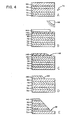
- FIGS 4A-4E The method of making the transistor as illustrated in Figure 2 in accordance with the present invention is shown in Figures 4A-4E.
- the drain layer 74, insulating layer 76, source layer 78, and second insulating layer 80 are formed in succession over the insulating substrate 72.
- a layer of aluminum 140 is formed over the insulating layer 80 of the metal-oxide-metal-oxide structure as shown in Figure 4B.
- a layer of positive photoresist 142 is formed over the aluminum layer 140.
- the aluminum has a thickness of between 100 and 300 nm (1000 and 3000 A), preferably 150 nm (1500 A).
- the photoresist has a thickness of between 1.5 and 3 pm, preferably 2 ⁇ m.
- a mask 144 is then placed over a portion of the positive photoresist layer 142.
- the positive photoresist layer 142 is then underexposed by using a light source 146 having the intensity of 300 millijoules/cm 2 .
- Mask 144 is then removed and the photoresist layer 142 is actively developed.
- Figure 4C illustrates the tapered surface 148 that results once layer 142 has been overdeveloped using an active developer solution as previously described.
- the configuration of Figure 4C is then subjected to an etching solution, e.g., consisting of one part deionized water (Di-H 2 0), one part nitric acid (HN0 3 ), three parts acetone (CH 3 00H) and fifteen parts phosphoric acid (H 3 P0 4 ).
- the etching solution will etch through the photoresist layer 142 and a portion of the aluminum layer 140.
- the tapered surface 148 in Figure 4C serves as a mask to create a tapered surface 143 in the aluminum layer 140 as illustrated in Figure 4D.
- the etched layer of aluminum 140 can now serve as a mask during plasma etching, preferably as described earlier.
- the structure shown in Figure 4E results once the plasma etching is complete.
- the layers 74, 76, 78 and 80 now form a surface 82 which is diagonal with respect to the substrate.
- the layer of aluminum 140 is then removed and the device is completed as described with respect to Figures 3F-31
- the thickness of the semiconductor material layers 22 and 84 is preferably greater between the uppermost layer of the structure and the gate insulator and thinner between the source and drain regions.
- the uppermost insulative layer 80 of the device of Figure 2 is formed to decouple the gate electrode 90 from the source region 80 by creating two capacitances in series. This diminishes the overall capacitance between the gate electrode 90 and the source region 80.
Landscapes
- Thin Film Transistor (AREA)
- Bipolar Transistors (AREA)
- Drying Of Semiconductors (AREA)
Claims (7)
Priority Applications (1)
| Application Number | Priority Date | Filing Date | Title |
|---|---|---|---|
| AT84113428T ATE35067T1 (de) | 1983-11-08 | 1984-11-07 | Kleinflaechiger duennfilmtransistor. |
Applications Claiming Priority (2)
| Application Number | Priority Date | Filing Date | Title |
|---|---|---|---|
| US549991 | 1983-11-08 | ||
| US06/549,991 US4543320A (en) | 1983-11-08 | 1983-11-08 | Method of making a high performance, small area thin film transistor |
Publications (2)
| Publication Number | Publication Date |
|---|---|
| EP0141425A1 EP0141425A1 (de) | 1985-05-15 |
| EP0141425B1 true EP0141425B1 (de) | 1988-06-08 |
Family
ID=24195275
Family Applications (1)
| Application Number | Title | Priority Date | Filing Date |
|---|---|---|---|
| EP84113428A Expired EP0141425B1 (de) | 1983-11-08 | 1984-11-07 | Kleinflächiger Dünnfilmtransistor |
Country Status (6)
| Country | Link |
|---|---|
| US (1) | US4543320A (de) |
| EP (1) | EP0141425B1 (de) |
| JP (1) | JPS60116135A (de) |
| AT (1) | ATE35067T1 (de) |
| CA (1) | CA1228180A (de) |
| DE (1) | DE3472036D1 (de) |
Families Citing this family (28)
| Publication number | Priority date | Publication date | Assignee | Title |
|---|---|---|---|---|
| JPS60186066A (ja) * | 1984-03-05 | 1985-09-21 | Semiconductor Energy Lab Co Ltd | 絶縁ゲイト型電界効果半導体装置およびその作製方法 |
| US4701996A (en) * | 1984-12-19 | 1987-10-27 | Calviello Joseph A | Method for fabricating edge channel FET |
| US4642665A (en) * | 1984-12-19 | 1987-02-10 | Eaton Corporation | Vertically layered MOMOM tunnel device |
| US4620207A (en) * | 1984-12-19 | 1986-10-28 | Eaton Corporation | Edge channel FET |
| FR2577715B1 (fr) * | 1985-02-19 | 1987-03-20 | Thomson Csf | Procede de realisation de deux structures mos a dielectriques juxtaposes differents et dopages differents et matrice a transfert de trame obtenue par ce procede |
| FR2586859B1 (fr) * | 1985-08-27 | 1987-11-20 | Thomson Csf | Procede de fabrication d'un transistor de commande pour ecran plat de visualisation et element de commande realise selon ce procede |
| US5064748A (en) * | 1987-04-27 | 1991-11-12 | Mcnc | Method for anisotropically hardening a protective coating for integrated circuit manufacture |
| US4826754A (en) * | 1987-04-27 | 1989-05-02 | Microelectronics Center Of North Carolina | Method for anisotropically hardening a protective coating for integrated circuit manufacture |
| JPH0283941A (ja) * | 1988-09-21 | 1990-03-26 | Fuji Xerox Co Ltd | 薄膜トランジスタの製造方法 |
| US5130263A (en) * | 1990-04-17 | 1992-07-14 | General Electric Company | Method for photolithographically forming a selfaligned mask using back-side exposure and a non-specular reflecting layer |
| US5356485A (en) * | 1992-04-29 | 1994-10-18 | The United States Of America As Represented By The Secretary Of Commerce | Intermetallic thermocouples |
| TW425637B (en) * | 1993-01-18 | 2001-03-11 | Semiconductor Energy Lab | Method of fabricating mis semiconductor device |
| US5452166A (en) * | 1993-10-01 | 1995-09-19 | Applied Magnetics Corporation | Thin film magnetic recording head for minimizing undershoots and a method for manufacturing the same |
| JP2003508807A (ja) * | 1999-08-31 | 2003-03-04 | イー−インク コーポレイション | 電子的に駆動されるディスプレイ用トランジスタ |
| EP1498957A1 (de) * | 2003-07-14 | 2005-01-19 | Fraunhofer-Gesellschaft zur Förderung der angewandten Forschung e.V. | Feldeffekttransistor und Verfahren zum Herstellen eines Feldeffekttransistors |
| US7629633B2 (en) * | 2004-05-20 | 2009-12-08 | Isaac Wing Tak Chan | Vertical thin film transistor with short-channel effect suppression |
| US20050258427A1 (en) * | 2004-05-20 | 2005-11-24 | Chan Isaac W T | Vertical thin film transistor electronics |
| US8383159B2 (en) * | 2004-10-27 | 2013-02-26 | Mcneil-Ppc, Inc. | Dosage forms having a microreliefed surface and methods and apparatus for their production |
| US20060088587A1 (en) * | 2004-10-27 | 2006-04-27 | Bunick Frank J | Dosage forms having a microreliefed surface and methods and apparatus for their production |
| US20070281022A1 (en) * | 2004-10-27 | 2007-12-06 | Bunick Frank J | Dosage forms having a microreliefed surface and methods and apparatus for their production |
| US20070190133A1 (en) * | 2004-10-27 | 2007-08-16 | Bunick Frank J | Dosage forms having a microreliefed surface and methods and apparatus for their production |
| US20060088586A1 (en) * | 2004-10-27 | 2006-04-27 | Bunick Frank J | Dosage forms having a microreliefed surface and methods and apparatus for their production |
| US20060088593A1 (en) * | 2004-10-27 | 2006-04-27 | Bunick Frank J | Dosage forms having a microreliefed surface and methods and apparatus for their production |
| US20060087051A1 (en) * | 2004-10-27 | 2006-04-27 | Bunick Frank J | Dosage forms having a microreliefed surface and methods and apparatus for their production |
| KR20140021914A (ko) * | 2012-08-13 | 2014-02-21 | 삼성전기주식회사 | 인쇄회로기판 제조 방법 |
| US9472649B1 (en) | 2015-12-09 | 2016-10-18 | The United States Of America As Represented By The Secretary Of The Air Force | Fabrication method for multi-zoned and short channel thin film transistors |
| JP2017139295A (ja) * | 2016-02-02 | 2017-08-10 | 東芝メモリ株式会社 | 基板処理装置、基板処理方法、および基板処理液 |
| CN105932066A (zh) * | 2016-06-07 | 2016-09-07 | 深圳市华星光电技术有限公司 | 金属氧化物薄膜晶体管及其制备方法 |
Family Cites Families (4)
| Publication number | Priority date | Publication date | Assignee | Title |
|---|---|---|---|---|
| US3669661A (en) * | 1970-03-06 | 1972-06-13 | Westinghouse Electric Corp | Method of producing thin film transistors |
| DE2117199C3 (de) * | 1971-04-08 | 1974-08-22 | Philips Patentverwaltung Gmbh, 2000 Hamburg | Verfahren zur Herstellung geätzter Muster in dünnen Schichten mit definierten Kantenprofilen |
| GB2052853A (en) * | 1979-06-29 | 1981-01-28 | Ibm | Vertical fet on an insulating substrate |
| IL61679A (en) * | 1979-12-13 | 1984-11-30 | Energy Conversion Devices Inc | Thin film,field effect transistor |
-
1983
- 1983-11-08 US US06/549,991 patent/US4543320A/en not_active Expired - Lifetime
-
1984
- 1984-11-07 EP EP84113428A patent/EP0141425B1/de not_active Expired
- 1984-11-07 AT AT84113428T patent/ATE35067T1/de not_active IP Right Cessation
- 1984-11-07 CA CA000467223A patent/CA1228180A/en not_active Expired
- 1984-11-07 DE DE8484113428T patent/DE3472036D1/de not_active Expired
- 1984-11-07 JP JP59234865A patent/JPS60116135A/ja active Pending
Also Published As
| Publication number | Publication date |
|---|---|
| ATE35067T1 (de) | 1988-06-15 |
| DE3472036D1 (en) | 1988-07-14 |
| US4543320A (en) | 1985-09-24 |
| EP0141425A1 (de) | 1985-05-15 |
| JPS60116135A (ja) | 1985-06-22 |
| CA1228180A (en) | 1987-10-13 |
Similar Documents
| Publication | Publication Date | Title |
|---|---|---|
| US4543320A (en) | Method of making a high performance, small area thin film transistor | |
| US4633284A (en) | Thin film transistor having an annealed gate oxide and method of making same | |
| US4746628A (en) | Method for making a thin film transistor | |
| US4253888A (en) | Pretreatment of photoresist masking layers resulting in higher temperature device processing | |
| US4547789A (en) | High current thin film transistor | |
| US7517738B2 (en) | Method for producing a semiconductor integrated circuit including a thin film transistor and a capacitor | |
| EP0063916B1 (de) | Integrierte Halbleiterschaltungen und Verfahren zu ihrer Herstellung | |
| US4620208A (en) | High performance, small area thin film transistor | |
| US4351894A (en) | Method of manufacturing a semiconductor device using silicon carbide mask | |
| US3994758A (en) | Method of manufacturing a semiconductor device having closely spaced electrodes by perpendicular projection | |
| US5518941A (en) | Maskless method for formation of a field implant channel stop region | |
| US5306653A (en) | Method of making thin film transistors | |
| US5880038A (en) | Method for producing semiconductor device | |
| US4371407A (en) | Method for producing semiconductor device | |
| EP0151224B1 (de) | Dünnschicht-Feldeffekttransistor mit kurzem Kanal und Verfahren zu seiner Herstellung | |
| EP0254071B1 (de) | Amorphe Dünnfilmtransistoranordnung | |
| EP0072660B1 (de) | Feldeffekttransistor und Verfahren zu dessen Herstellung | |
| EP0476844A1 (de) | Verfahren zur Herstellung von Josephson-Tunnelübergängen mit genauer Übergangsbereichskontrolle | |
| EP0095654B1 (de) | Verfahren zum Herstellen einer Halbleiteranordnung mit einem Schritt zum Mustern einer Leiterschicht | |
| EP0068843A2 (de) | Verfahren zum Herstellen eines Leiters mit einem gewünschten Muster auf einem Halbleitersubstrat | |
| JPS61224360A (ja) | 電界効果トランジスタの製造方法 | |
| JP3055782B2 (ja) | 薄膜トランジスタの製造方 | |
| JPH05335578A (ja) | 薄膜トランジスタの製造方法 | |
| CA1234227A (en) | High performance, small area thin film transistor | |
| KR950006491B1 (ko) | 수직형 박막트랜지스터의 제조방법 |
Legal Events
| Date | Code | Title | Description |
|---|---|---|---|
| PUAI | Public reference made under article 153(3) epc to a published international application that has entered the european phase |
Free format text: ORIGINAL CODE: 0009012 |
|
| AK | Designated contracting states |
Designated state(s): AT BE CH DE FR GB IT LI LU NL SE |
|
| 17P | Request for examination filed |
Effective date: 19850620 |
|
| 17Q | First examination report despatched |
Effective date: 19870327 |
|
| GRAA | (expected) grant |
Free format text: ORIGINAL CODE: 0009210 |
|
| AK | Designated contracting states |
Kind code of ref document: B1 Designated state(s): AT BE CH DE FR GB IT LI LU NL SE |
|
| PG25 | Lapsed in a contracting state [announced via postgrant information from national office to epo] |
Ref country code: NL Effective date: 19880608 Ref country code: LI Effective date: 19880608 Ref country code: IT Free format text: LAPSE BECAUSE OF FAILURE TO SUBMIT A TRANSLATION OF THE DESCRIPTION OR TO PAY THE FEE WITHIN THE PRESCRIBED TIME-LIMIT;WARNING: LAPSES OF ITALIAN PATENTS WITH EFFECTIVE DATE BEFORE 2007 MAY HAVE OCCURRED AT ANY TIME BEFORE 2007. THE CORRECT EFFECTIVE DATE MAY BE DIFFERENT FROM THE ONE RECORDED. Effective date: 19880608 Ref country code: CH Effective date: 19880608 Ref country code: BE Effective date: 19880608 Ref country code: AT Effective date: 19880608 |
|
| REF | Corresponds to: |
Ref document number: 35067 Country of ref document: AT Date of ref document: 19880615 Kind code of ref document: T |
|
| PG25 | Lapsed in a contracting state [announced via postgrant information from national office to epo] |
Ref country code: SE Effective date: 19880630 |
|
| REF | Corresponds to: |
Ref document number: 3472036 Country of ref document: DE Date of ref document: 19880714 |
|
| ET | Fr: translation filed | ||
| REG | Reference to a national code |
Ref country code: CH Ref legal event code: PL |
|
| NLV1 | Nl: lapsed or annulled due to failure to fulfill the requirements of art. 29p and 29m of the patents act | ||
| PG25 | Lapsed in a contracting state [announced via postgrant information from national office to epo] |
Ref country code: LU Free format text: LAPSE BECAUSE OF NON-PAYMENT OF DUE FEES Effective date: 19881130 |
|
| PLBE | No opposition filed within time limit |
Free format text: ORIGINAL CODE: 0009261 |
|
| STAA | Information on the status of an ep patent application or granted ep patent |
Free format text: STATUS: NO OPPOSITION FILED WITHIN TIME LIMIT |
|
| 26N | No opposition filed | ||
| PGFP | Annual fee paid to national office [announced via postgrant information from national office to epo] |
Ref country code: GB Payment date: 19911017 Year of fee payment: 8 |
|
| PGFP | Annual fee paid to national office [announced via postgrant information from national office to epo] |
Ref country code: FR Payment date: 19911120 Year of fee payment: 8 |
|
| PGFP | Annual fee paid to national office [announced via postgrant information from national office to epo] |
Ref country code: DE Payment date: 19911128 Year of fee payment: 8 |
|
| PG25 | Lapsed in a contracting state [announced via postgrant information from national office to epo] |
Ref country code: GB Effective date: 19921107 |
|
| GBPC | Gb: european patent ceased through non-payment of renewal fee |
Effective date: 19921107 |
|
| PG25 | Lapsed in a contracting state [announced via postgrant information from national office to epo] |
Ref country code: FR Effective date: 19930730 |
|
| PG25 | Lapsed in a contracting state [announced via postgrant information from national office to epo] |
Ref country code: DE Effective date: 19930803 |
|
| REG | Reference to a national code |
Ref country code: FR Ref legal event code: ST |