EP0142310A1 - Elektrische Anordnung mit Ladungsspeicher-Detektor - Google Patents
Elektrische Anordnung mit Ladungsspeicher-Detektor Download PDFInfo
- Publication number
- EP0142310A1 EP0142310A1 EP84307439A EP84307439A EP0142310A1 EP 0142310 A1 EP0142310 A1 EP 0142310A1 EP 84307439 A EP84307439 A EP 84307439A EP 84307439 A EP84307439 A EP 84307439A EP 0142310 A1 EP0142310 A1 EP 0142310A1
- Authority
- EP
- European Patent Office
- Prior art keywords
- samples
- detector
- waveform
- negative
- positive
- Prior art date
- Legal status (The legal status is an assumption and is not a legal conclusion. Google has not performed a legal analysis and makes no representation as to the accuracy of the status listed.)
- Granted
Links
Images


Classifications
-
- G—PHYSICS
- G08—SIGNALLING
- G08B—SIGNALLING SYSTEMS, e.g. PERSONAL CALLING SYSTEMS; ORDER TELEGRAPHS; ALARM SYSTEMS
- G08B17/00—Fire alarms; Alarms responsive to explosion
- G08B17/06—Electric actuation of the alarm, e.g. using a thermally-operated switch
Definitions
- the invention relates to electrical circuit arrangements and more particularly to temperature-responsive electrical circuit arrangements.
- One such circuit arrangement to be described by way of example is for use with a temperature detector of the type whose capability of accepting an electrical charge increases with temperature; the circuit arrangement determines the electrical state of the detector and thus can determine whether its temperature is excessive.
- a temperature detector may advantageously be of linear form so as to be mountable around an area whose temperature is to be monitored.
- an electrical circuit arrangement for monitoring the state of detecting means whose charge storage capability increases under predetermined conditions comprising driving means operative to apply an alternately positive and negative test waveform to the detecting means, and digital testing means operative at predetermined time instants during positive and negative half cycles of the test waveform to determine assymmetry of the waveform caused by an increase in the charge storage capabilities of the detecting means.
- a method of sensing temperature increase using a temperature detector in the form of coaxial conductors separated by temperature-responsive material which increases the charge storage capacity between the conductors as its temperature increases comprising the steps of applying an alternately positive and negative test waveform to the detector, and sampling the test waveform at predetermined time instants during positive and negative half cycles thereof to determine assymmetry of the waveform caused by an increase in its charge storage capacity of the detector.
- the linear temperature detector comprises an elongated conductive sheath 12 of circular cross-section having an inner coaxial conductor 14.
- An insulating material separates the conductors 12 and 14 and is such that the capability of the detector to accept an electrical charge increases with temperature.
- the detector may be of the form as sold by the Applicants under the Trade Mark FIREWIRE.
- one of the conductors of the detector 10 is held at ground potential and the other is subjected to a rectangular waveform which renders it alternately positive and negative (swinging in this example between plus 5 and minus 5 volts).
- the impedance of the detector is high and the voltage across the detector will swing between plus 5 and minus 5 volts in correspondence with the applied waveform.
- the detector's resistance will decrease and its capability of accepting charge will increase.
- a fault condition (such as caused by contamination or mechanical damage to the detector), which causes the electrical resistance between the conductors 12 and 14 to decrease, will have a different effect.
- the inequality between the decrease in voltage across the detector during positive half cycles and the decrease in that voltage during negative half cycles will not be so great because the detector's capability of accepting charge is not increased and therefore the increased volt drop effect of the charging current is not present.
- the circuit arrangement to be described uses this effect to detect and signal such a fault.
- the circuit arrangment is (in this example) powered by a 28 volt DC supply on lines 16 and 18.
- a regulator and converter arrangement 20 produces a stabilised DC output on lines 22 (0 volts), 24 (plus 5 volts) and 26 (minus 5 volts).
- Line 22 is connected to conductor 12 of the detector 10 while lines 24 and 26 energise the plus 5 volt and minus 5 volt rails of a driver circuit 28 via connections not shown.
- the circuit 28 comprises transistors 30 and 32 having their collectors connected to feed the conductor 12 of the detector 10 by respective resistors 34 and 36; these are the unequal resistors referred to above and may have resistances of 2700 and 430 ohms for example.
- the transistors are rendered conductive alternately, thus applying a rectangular waveform, swinging between plus 5 volts and minus 5 volts, to the conductor 14 of the detector 10 via line 38.
- the transistors 30 and 32 are rendered conductive alternately by a 400 Hz signal from a divider and timing pulse encoder unit 38 on a line 40.
- the unit 38 is driven by_a 3.2 KHz oscillator 41 whose output frequency is divided down by 8 in the unit 38.
- the waveform shown in Figure 2A is thus the output waveform of the driver circuit 28 and is therefore the nominal waveform on line 42 (Fig. 1) when the detector 10 is cold so as to have effectively no charge storage capability.
- a reference selector 44 provides a sequence of voltage references against which the voltage across the detector 10 during each half cycle is compared.
- the reference selector 44 comprises a potential divider of resistors connected between a plus 5 volt rail energised from line 24 and a minus 5 volt rail energised from line 26.
- the resistors are selected so as to provide tapped reference voltages of plus 3 volts, plus 1.35 volts, plus 0.5 volts, minus 2.35 volts, and minus 3.5 volts.
- the reference selector 44 is controlled in correspondence with the output of the divider and timing pulse encoder unit 38 via lines 70.
- the lines 70 therefore select each of the reference voltages in turn and the corresponding reference voltage is fed to a comparator 72 on a line 74.
- Waveform 2B shows the sequence of the voltage references.
- the selector 44 (Fig.l) produces reference voltages of +1.35 volts and +0.5 volts alternately for successive positive half cycles of waveform 2A.
- a line 75 (Fig.l) causes the selector 44 to select and produce the reference of +3.0 volts instead of plus 1.35 volts (though during the intervening positive half cycles, the reference voltage continues to be plus 0.5 volts), all as shown in waveform 2B.
- the selector 44 selects the reference voltage of minus 3.5 volts for the first half of the half cycle and minus 2.35 volts for the remainder of that half cycle.
- the reference voltages applied during the negative half cycles of the drive waveform are unaffected by any fault condition.
- the comparator 72 carries out a comparison of the voltage across the detector 10 in line 42 with the reference voltage waveform 2B on line 74.
- the output of comparator 72 is in the form of a binary signal, that is, "1" or "0". Thus, if the voltage on line 42 is more negative than the voltage on line 74, comparator 72 produces a “1” output on a line 78 but a "0" output is produced in the reverse condition.
- Line 78 is connected in common to four "smoother" units 80,82,84 and 86, each of which comprises a respective shift register whose outputs are fed into suitable logic circuitry driving an output latch. Each shift register is clocked by a respective sequence of clock signals derived from the unit 38 via lines 70 and a timing pulse generator 87.
- the smoother unit 80 comprises a shift register 88 having eight stages, the stage outputs being fed into a logic unit 90 driving a latch 92.
- the shift register 88 is clocked by clock pulses TP1A, these being received from the unit 87 on a line 93.
- pulses TPIA occur during alternate half cycles of the reference waveform 2B. Therefore, each pulse TP1A clocks into the shift register 88 a binary signal (on line 78) having a value depending on whether the voltage across the detector 10 is above or below the plus 0.5 volt reference.
- the pulses TP1A normally occur three quarters of the way through each alternate positive half cycle. However, they can occur at a different position, one quarter of the way through each alternate half cycle, as shown dotted.
- the smoother 88 therefore sets the latch 92 after eight consecutive pulses TP1A (arranged over 16 positive half cycles) have occurred, at each of which the waveform from the detector is below 0.5 volts.
- Smoother 82 is again in the form of a shift register 93, this time having four stages which are connected to logic 94.
- the smoother 82 is clocked by clock pulses TP1B received from the unit 87.
- the pulses TPIB occur during alternate positive half cycles, the half cycles during which the pulses TP1A do not occur.
- Each pulse TPIB occurs at a point three quarters of the way through its respective half cycle.
- Each pulse TP1B therefore tests whether or not the waveform from the detector is above either plus 1.35 volts or plus 3.00 volts depending on the particular reference level during the half cycle.
- the selector 44 alters the reference level on line 74 during alternate half cycles from plus 1.35 volts to plus 3.0 volts and these alternate half cycles are synchronised with the pulses TP1B. If, at each occurence of a pulse TP1B, the comparator 72 determines that the waveform from the detector 10 is more positive than the reference waveform on line 74, it produces a "0" output which is clocked into the register 93 by the pulse TP1B. When four such consecutive outputs are clocked into the register, the logic unit 94 produces a signal RE on a line 96 which is fed to an AND gate 98 connected to a reset line 100.
- Smoother 84 comprises a shift register 101 having four stages which are all connected to logic 102.
- Register 101 is clocked by pulses TP2 from the unit 87 and as shown in Figure 2, these occur during each negative half cycle of the drive waveform. Each occurs one quarter of the way through its respective half cycle and thus occurs when the reference level on line 74 is minus 3.5 volts. If comparator 72 determines that the waveform from the detector 10 is more negative than minus 3.5 volts, line 78 will carry a "1" when each pulse TP2 occurs and this will be clocked into the register 101. If four such consecutive binary signals are produced, the logic 102 produces a latched output CH on a line 104.
- the detector waveform is not more negative than minus 3.5 volts when each pulse TP2 occurs, binary "0" signals will be produced on line 78 and the logic 102 will be latched into a state in which it produces a signal CH on a line 106.
- the signals CH are passed through the gate 98 onto the reset line 100, while the signals CH are passed to the unit 87 where they shift the time of occurrence of the pulses TP1A to the dotted position shown in waveform 2A.
- Smoother 86 is in the form of a four stage shift register 107 whose stages are connected to logic 108 which controls a latch 110.
- the shift register 107 is clocked by pulses TP3 from the unit 87 and as shown in waveform 2A these occur during every negative half cycle of the drive waveform 2A, each one occurring at three quarters of the way through the half cycle.
- each pulse TP3 occurs when the reference level on line 74 is at minus 2.2 volts. If the waveform from the detector is more negative than minus 2.2 volts when each pulse TP3 occurs, a binary "1" will be clocked into the shift register 107. After four such consecutive binary signals, the logic 108 will produce a signal FA.
- Latches 92 and 110 are connected to be reset by the reset line 100.
- latch 92 When set, latch 92 produces a fire warning signal on line 112. Similarly, when set, the latch 110 produces a fault warning signal on a line 114.
- the first condition to be considered will be when the detector 10 is cold or at normal ambient temperature and with no fault.
- the waveform produced by the detector that is, the waveform on line 42,--can therefore be considered to be as shown in Figure 2A, that is, substantially unchanged from the drive waveform. Therefore, during each pulse TP1A, the comparator 72 will produce a binary "0" signal and the latch 90 will therefore not be set and no signal will be produced on line 112.
- the comparator 72 will also be producing a binary "0" signal because the waveform from the detector will be more positive than plus 1.35 or plus 3.00 volts. After four such binary signals, logic 94 will therefore be set to produce a signal RE on the line 96 which will be fed to AND gate 98.
- comparator 72 will determine that the waveform from the detector is more negative than the reference level and will produce a binary "I". Four such binary signals will thus cause the latch 102 to produce the signal CH and this will be fed to gate 98.Line 100 will therefore be energised to carry a RESET level.
- the comparator 72 will determine that the waveform from the detector is more negative than the reference level and will again produce a "1" output. Four such binary signals will cause the logic 108 to produce a signal FA, and the latch 110 will therefore not be set.
- the effect therefore, is that neither a fire warning nor a fault warning is produced.
- the RESET level on line 100 therefore has no effect because the latches 92 and 110 are already in the reset state.
- the comparator 72 will be producing a binary "1" output when each pulse TP1A occurs. After eight such signals (16 positive half cycles), the latch 92 will be set and will produce a fire warning signal on line 112.
- the comparator 72 will also be producing a "1" output, but because of the inverter 79, latch 94 will not be set and no signal RE will be produced.
- the comparator 72 will also produce a binary "1" output and therefore latch 110 will not be set into the FAULT condition and no fault warning will be produced on line 114.
- the waveform from the detector 10 will change back towards that shown in Figure 2A. If the level of the detector waveform during positive half cycles remains above plus 1.35 volts for four consecutive positive half cycles, the corresponding pulses TP1B will cause the inverter 79 to clock binary "1" signals into the register 93 and latch 94 will thus produce a RE signal on line 96 to the AND gate 98. Provided that the waveform from the detector is also more negative than minus 3.5 volts during four consecutive half cycles, the corresponding pulses TP2 will clock binary "1" signals into the register 101 and the logic 102 will thus produce a CH output to AND gate 98. Line 100 will thus carry a RESET signal which will reset the latch 92 (latch 110 already being in the reset state). The fire signal on line 112 will thus be removed.
- the waveform on line 128 may (at least initially) become as shown in Figure 2D. This shows that the voltage three quarters of the way through each positive half cycle has not dropped below plus 0.5 volts. Therefore, the comparator 72 will not be producing binary "1" outputs when pulses TP1A occur three quarters of the way through each alternate positive half cycle. Latch 92 would therefore not be set into the FIRE state and no fire warning would be produced. Register 101 deals with this condition. As is shown in waveform 2B, the voltage of the detector waveform during negative half cycles is more positive than minus 3.5 volts.
- Each pulse TP2 will therefore cause a binary "0" to be clocked into the register and logic 102 will therefore produce a CH output on line 106.
- This has the effect of causing the unit 87 to shift the positions of the pulses TP1A to the positions shown dotted in waveform 2A.
- the waveform shown in Figure 2D is more negative than the reference level of 0.5 volts, and thus eight pulses TP1A (in the dotted position) will cause eight binary "1" signals to be clocked in to register 88 so as to set the latch 92 into the FIRE state, producing a fire warning on line 112.
- Figure 2E shows the form which the waveform from the detector can take under such conditions.
- the voltage remains above 0.5 volts during positive half cycles and therefore the latch 92 will not be set into the FIRE state and no fire warning will be produced.
- the voltage of the waveform 2E is more negative than plus 1.35 volts so logic 94 is not set into the RE state.
- the detector waveform is less negative than minus 3.5 volts, so the logic 101 will produce a CH output on line 106 after four such half cycles. However, the resultant shifting of the pulses TP1A to the dotted position shown in waveform 2A will not have any effect.
- waveform 2E is less negative than minus 2.2 volts and therefore binary "1" signals will be fed into register 86, and four such binary signals will cause the latch 110 to be set into the FAULT condition so as to produce a fault warning on line 114.
- the fault warning on line 114 is also fed via line 75 to the selector 44 and has the effect of changing the reference level applied to the comparator 72 on line 74 during alternate positive half cycles from plus 1.35 volts to plus 3.00 volts. Therefore, when the fault condition disappears, register 93 will not set the logic 94 into the RE state until the waveform from the detector 10 has been more positive than plus 3 volts for four pulses TP1B. Provided that the waveform from the detector 10 is also more negative than minus 3.5 volts, register 101 will also set the logic 102 to produce a CH output. AND gate 98 will therefore produce a RESET signal on line 100 which will reset the latch 110 and remove the fault warning from line 114.
- the output of integrator 130 can therefore be used to provide a supplementary indication of the state of the detector 10.
- this output can be fed on a line 132 to a suitable indicator .
- the indication given by the indicator indicates the "trend" detected by the detector 10.
- a slope unit 136 detects such a condition and produces a fault indication on a line 138. This is fed to the register 107 and immediately switches the register to produce an output which sets latch 110 into the FAULT condition, thus providing a back-up to the fault monitoring provided by the pulses TP3.
- a reset unit 140 produces a reset signal on a line 142 for resetting the various logic units of the system when the power is first switched on.
- a line 122 interconnects the fault warning line 112 with an inhibit input of latch 110. Therefore, if latch 92 is set into the FIRE condition, as a result of the waveform from the detector being more negative than plus 0.5 volts during eight alternate positive half cycles, not only will a fire warning be produced on line 112 but latch 110 will be prevented from being switched into the FAULT state even if the detector waveform has become less negative than minus 2.2 volts during four pulses TP3. Similarly a line 123 prevents a fire warning, if latch 110 is in the "fault" state.
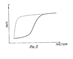
- an output is taken from the collector of transistor 32 on a line 128 and this is fed into an integrator 130 whose output therefore represents the inverse integral of the positive half of the waveform from the detector 10.
- Figure 3 shows in full line the normal shape of the waveform produced by the integrator 130, the horizontal axis representing either time or temperature provided that the temperature is rising slowly. However, if the detector is subjected to a very fierce fire, it is found that the output of integrator 130 changes to the dotted form the power supply to the various units of the system have been omitted for clarity.
Landscapes
- Business, Economics & Management (AREA)
- Emergency Management (AREA)
- Physics & Mathematics (AREA)
- General Physics & Mathematics (AREA)
- Fire-Detection Mechanisms (AREA)
- Measuring Temperature Or Quantity Of Heat (AREA)
- Testing Or Calibration Of Command Recording Devices (AREA)
- Fire Alarms (AREA)
Applications Claiming Priority (2)
| Application Number | Priority Date | Filing Date | Title |
|---|---|---|---|
| GB8329473 | 1983-11-04 | ||
| GB08329473A GB2149167B (en) | 1983-11-04 | 1983-11-04 | Electrical circuit arrangements in fire alarms |
Publications (2)
| Publication Number | Publication Date |
|---|---|
| EP0142310A1 true EP0142310A1 (de) | 1985-05-22 |
| EP0142310B1 EP0142310B1 (de) | 1988-01-20 |
Family
ID=10551230
Family Applications (1)
| Application Number | Title | Priority Date | Filing Date |
|---|---|---|---|
| EP84307439A Expired EP0142310B1 (de) | 1983-11-04 | 1984-10-29 | Elektrische Anordnung mit Ladungsspeicher-Detektor |
Country Status (7)
| Country | Link |
|---|---|
| US (1) | US4628301A (de) |
| EP (1) | EP0142310B1 (de) |
| JP (1) | JPS60133318A (de) |
| BR (1) | BR8405558A (de) |
| DE (1) | DE3468950D1 (de) |
| GB (1) | GB2149167B (de) |
| IN (1) | IN163007B (de) |
Cited By (3)
| Publication number | Priority date | Publication date | Assignee | Title |
|---|---|---|---|---|
| FR2588081A1 (fr) * | 1985-09-27 | 1987-04-03 | Abg Semca | Procede de surveillance de temperature a l'aide d'un detecteur a fil |
| FR2608815A1 (fr) * | 1986-12-17 | 1988-06-24 | Aerospatiale | Systeme pour detecter la surchauffe d'ambiance de differents espaces |
| FR2689664A1 (fr) * | 1992-04-01 | 1993-10-08 | Aerospatiale | Appareil de contrôle de boucle de surveillance d'air chaud. |
Families Citing this family (3)
| Publication number | Priority date | Publication date | Assignee | Title |
|---|---|---|---|---|
| US5663710A (en) * | 1995-07-18 | 1997-09-02 | Jaycor | Backscatter-type visibility detection |
| US6384731B1 (en) | 2001-02-20 | 2002-05-07 | Ronald L. Sutherland | System for detecting a fire event |
| US11879787B2 (en) * | 2020-10-06 | 2024-01-23 | Kidde Technologies, Inc. | Heat sensor cable with ceramic coil and eutectic salt between inner and outer conductors |
Citations (3)
| Publication number | Priority date | Publication date | Assignee | Title |
|---|---|---|---|---|
| DE1247180B (de) * | 1960-06-09 | 1967-08-10 | Graviner Manufacturing Co | UEberhitzungs- und Feuerwarnsystem |
| DE1261026B (de) * | 1965-01-09 | 1968-02-08 | Graviner Colnbroock Ltd | UEberhitzungs- und Feuerwarnsystem |
| US3540041A (en) * | 1967-07-24 | 1970-11-10 | Whittaker Corp | Fire warning system improvement |
Family Cites Families (13)
| Publication number | Priority date | Publication date | Assignee | Title |
|---|---|---|---|---|
| GB953166A (de) * | ||||
| GB872042A (en) * | 1956-10-01 | 1961-07-05 | Sperry Rand Corp | Temperature responsive apparatus |
| GB1151691A (en) * | 1965-01-09 | 1969-05-14 | Graviner Colnbrook Ltd | Improvements in or relating to Electrical Circuits |
| GB1006208A (en) * | 1962-11-20 | 1965-09-29 | Specialties Dev Corp | Heat detecting apparatus |
| GB1013797A (en) * | 1962-12-17 | 1965-12-22 | Pyrene Co Ltd | Improvements in or relating to fire-detection circuits |
| CH468682A (de) * | 1967-06-26 | 1969-02-15 | Cerberus Ag | Feuermeldeanlage |
| JPS5275298A (en) * | 1975-12-19 | 1977-06-24 | Omron Tateisi Electronics Co | Fire receiver |
| DE2641574A1 (de) * | 1976-09-13 | 1978-03-16 | Siemens Ag | Zylinderkondensator |
| DE2804523C3 (de) * | 1978-02-02 | 1981-12-03 | Preussag Ag Feuerschutz, 2060 Bad Oldesloe | Brandmeldeeinrichtung |
| JPS577102Y2 (de) * | 1978-02-16 | 1982-02-10 | ||
| GB2065348B (en) * | 1979-12-07 | 1983-06-22 | Rca Security Systems Ltd | Multiple alarm condition detection and signalling |
| JPS586139A (ja) * | 1981-07-02 | 1983-01-13 | Seiko Epson Corp | 半導体装置の製造方法 |
| EP0087308A2 (de) * | 1982-02-23 | 1983-08-31 | Dreamland Electrical Appliances P.L.C. | Temperaturüberwachungssysteme |
-
1983
- 1983-11-04 GB GB08329473A patent/GB2149167B/en not_active Expired
-
1984
- 1984-10-29 EP EP84307439A patent/EP0142310B1/de not_active Expired
- 1984-10-29 DE DE8484307439T patent/DE3468950D1/de not_active Expired
- 1984-10-30 US US06/666,399 patent/US4628301A/en not_active Expired - Fee Related
- 1984-10-31 BR BR8405558A patent/BR8405558A/pt not_active IP Right Cessation
- 1984-11-02 IN IN822/MAS/84A patent/IN163007B/en unknown
- 1984-11-05 JP JP59231444A patent/JPS60133318A/ja active Granted
Patent Citations (3)
| Publication number | Priority date | Publication date | Assignee | Title |
|---|---|---|---|---|
| DE1247180B (de) * | 1960-06-09 | 1967-08-10 | Graviner Manufacturing Co | UEberhitzungs- und Feuerwarnsystem |
| DE1261026B (de) * | 1965-01-09 | 1968-02-08 | Graviner Colnbroock Ltd | UEberhitzungs- und Feuerwarnsystem |
| US3540041A (en) * | 1967-07-24 | 1970-11-10 | Whittaker Corp | Fire warning system improvement |
Cited By (4)
| Publication number | Priority date | Publication date | Assignee | Title |
|---|---|---|---|---|
| FR2588081A1 (fr) * | 1985-09-27 | 1987-04-03 | Abg Semca | Procede de surveillance de temperature a l'aide d'un detecteur a fil |
| EP0218519A1 (de) * | 1985-09-27 | 1987-04-15 | Thomson-Csf | Temperaturkontrollverfahren mit Hilfe eines Strangthermometers |
| FR2608815A1 (fr) * | 1986-12-17 | 1988-06-24 | Aerospatiale | Systeme pour detecter la surchauffe d'ambiance de differents espaces |
| FR2689664A1 (fr) * | 1992-04-01 | 1993-10-08 | Aerospatiale | Appareil de contrôle de boucle de surveillance d'air chaud. |
Also Published As
| Publication number | Publication date |
|---|---|
| DE3468950D1 (en) | 1988-02-25 |
| JPS60133318A (ja) | 1985-07-16 |
| IN163007B (de) | 1988-07-30 |
| GB2149167A (en) | 1985-06-05 |
| US4628301A (en) | 1986-12-09 |
| GB8329473D0 (en) | 1983-12-07 |
| GB2149167B (en) | 1987-04-08 |
| EP0142310B1 (de) | 1988-01-20 |
| JPH058764B2 (de) | 1993-02-03 |
| BR8405558A (pt) | 1985-09-10 |
Similar Documents
| Publication | Publication Date | Title |
|---|---|---|
| US8163411B2 (en) | Abnormality detection apparatus for battery pack | |
| JP3323498B2 (ja) | 充放電中にバッテリを監視するシステム | |
| CA1173905A (en) | Fault anticipation apparatus for high voltage electrical equipment | |
| US4516076A (en) | Fault detection arrangement for relay switching system | |
| CN1171092C (zh) | Ic测试装置 | |
| US7280333B2 (en) | Method and device for short circuit or open load detection | |
| KR940701546A (ko) | 배터리를 충전하고 테스트하는 방법 및 장치 | |
| US4583036A (en) | Charging system diagnostic device | |
| US4421976A (en) | System for monitoring heater elements of electric furnaces | |
| EP0273196B1 (de) | Mehrniveau-Musterdetektor für ein einzelnes Signal | |
| US4628301A (en) | Electrical circuit arrangements | |
| US4342112A (en) | Error checking circuit | |
| US4697142A (en) | Printed circuit conductor test system | |
| US4743847A (en) | Printed circuit conductor test system | |
| EP0102659B1 (de) | Waschmaschinengeschwindigkeitskontrollschaltung | |
| EP3062299A1 (de) | Vorrichtung und verfahren zur erkennung und anpassung an einem abschlusswiderstand und zur erdungsfehlerlokalisierung | |
| US5621742A (en) | Method and apparatus for testing semiconductor integrated circuit devices | |
| EP0317578A1 (de) | Drei-stände-schaltungstestvorrichtung | |
| JPH10511470A (ja) | 試験可能回路及び試験方法 | |
| CA1183209A (en) | Telephone cable splicers test set and method of testing | |
| EP0789244B1 (de) | Elektronisches Signalmessgerät und -Verfahren zur Erfassung und Anzeige kurzzeitiger analoger Signalereignisse | |
| RU2029968C1 (ru) | Устройство для контроля сопротивления изоляции электрических цепей | |
| JPH0124273B2 (de) | ||
| JPH0646522A (ja) | 遮断器用操作制御回路の常時監視装置 | |
| JPH0530223B2 (de) |
Legal Events
| Date | Code | Title | Description |
|---|---|---|---|
| PUAI | Public reference made under article 153(3) epc to a published international application that has entered the european phase |
Free format text: ORIGINAL CODE: 0009012 |
|
| AK | Designated contracting states |
Designated state(s): BE CH DE FR IT LI NL SE |
|
| 17P | Request for examination filed |
Effective date: 19851008 |
|
| 17Q | First examination report despatched |
Effective date: 19861203 |
|
| ITF | It: translation for a ep patent filed | ||
| GRAA | (expected) grant |
Free format text: ORIGINAL CODE: 0009210 |
|
| AK | Designated contracting states |
Kind code of ref document: B1 Designated state(s): BE CH DE FR IT LI NL SE |
|
| PG25 | Lapsed in a contracting state [announced via postgrant information from national office to epo] |
Ref country code: NL Effective date: 19880120 |
|
| PG25 | Lapsed in a contracting state [announced via postgrant information from national office to epo] |
Ref country code: SE Effective date: 19880131 |
|
| REF | Corresponds to: |
Ref document number: 3468950 Country of ref document: DE Date of ref document: 19880225 |
|
| ET | Fr: translation filed | ||
| NLV1 | Nl: lapsed or annulled due to failure to fulfill the requirements of art. 29p and 29m of the patents act | ||
| PLBE | No opposition filed within time limit |
Free format text: ORIGINAL CODE: 0009261 |
|
| STAA | Information on the status of an ep patent application or granted ep patent |
Free format text: STATUS: NO OPPOSITION FILED WITHIN TIME LIMIT |
|
| 26N | No opposition filed | ||
| REG | Reference to a national code |
Ref country code: CH Ref legal event code: PFA Free format text: KIDDE-GRAVINER LIMITED |
|
| PGFP | Annual fee paid to national office [announced via postgrant information from national office to epo] |
Ref country code: BE Payment date: 19901129 Year of fee payment: 7 |
|
| REG | Reference to a national code |
Ref country code: FR Ref legal event code: CD Ref country code: FR Ref legal event code: CA |
|
| ITTA | It: last paid annual fee | ||
| PG25 | Lapsed in a contracting state [announced via postgrant information from national office to epo] |
Ref country code: BE Effective date: 19911031 |
|
| BERE | Be: lapsed |
Owner name: KIDDE-GRAVINER LTD Effective date: 19911031 |
|
| PGFP | Annual fee paid to national office [announced via postgrant information from national office to epo] |
Ref country code: FR Payment date: 19990324 Year of fee payment: 15 |
|
| PGFP | Annual fee paid to national office [announced via postgrant information from national office to epo] |
Ref country code: CH Payment date: 19990329 Year of fee payment: 15 |
|
| PG25 | Lapsed in a contracting state [announced via postgrant information from national office to epo] |
Ref country code: LI Free format text: LAPSE BECAUSE OF NON-PAYMENT OF DUE FEES Effective date: 19991031 Ref country code: CH Free format text: LAPSE BECAUSE OF NON-PAYMENT OF DUE FEES Effective date: 19991031 |
|
| REG | Reference to a national code |
Ref country code: CH Ref legal event code: PL |
|
| PG25 | Lapsed in a contracting state [announced via postgrant information from national office to epo] |
Ref country code: FR Free format text: LAPSE BECAUSE OF NON-PAYMENT OF DUE FEES Effective date: 20000630 |
|
| REG | Reference to a national code |
Ref country code: FR Ref legal event code: ST |
|
| PGFP | Annual fee paid to national office [announced via postgrant information from national office to epo] |
Ref country code: DE Payment date: 20031103 Year of fee payment: 20 |