EP0142450A2 - Vorrichtung zum Anbringen von dünnen dielektrischen Lagen an Festkörperoberflächen - Google Patents
Vorrichtung zum Anbringen von dünnen dielektrischen Lagen an Festkörperoberflächen Download PDFInfo
- Publication number
- EP0142450A2 EP0142450A2 EP84402319A EP84402319A EP0142450A2 EP 0142450 A2 EP0142450 A2 EP 0142450A2 EP 84402319 A EP84402319 A EP 84402319A EP 84402319 A EP84402319 A EP 84402319A EP 0142450 A2 EP0142450 A2 EP 0142450A2
- Authority
- EP
- European Patent Office
- Prior art keywords
- tube
- zone
- treated
- plasma
- electrode
- Prior art date
- Legal status (The legal status is an assumption and is not a legal conclusion. Google has not performed a legal analysis and makes no representation as to the accuracy of the status listed.)
- Granted
Links
Images

Classifications
-
- H—ELECTRICITY
- H01—ELECTRIC ELEMENTS
- H01J—ELECTRIC DISCHARGE TUBES OR DISCHARGE LAMPS
- H01J37/00—Discharge tubes with provision for introducing objects or material to be exposed to the discharge, e.g. for the purpose of examination or processing thereof
- H01J37/32—Gas-filled discharge tubes
- H01J37/32431—Constructional details of the reactor
-
- C—CHEMISTRY; METALLURGY
- C23—COATING METALLIC MATERIAL; COATING MATERIAL WITH METALLIC MATERIAL; CHEMICAL SURFACE TREATMENT; DIFFUSION TREATMENT OF METALLIC MATERIAL; COATING BY VACUUM EVAPORATION, BY SPUTTERING, BY ION IMPLANTATION OR BY CHEMICAL VAPOUR DEPOSITION, IN GENERAL; INHIBITING CORROSION OF METALLIC MATERIAL OR INCRUSTATION IN GENERAL
- C23C—COATING METALLIC MATERIAL; COATING MATERIAL WITH METALLIC MATERIAL; SURFACE TREATMENT OF METALLIC MATERIAL BY DIFFUSION INTO THE SURFACE, BY CHEMICAL CONVERSION OR SUBSTITUTION; COATING BY VACUUM EVAPORATION, BY SPUTTERING, BY ION IMPLANTATION OR BY CHEMICAL VAPOUR DEPOSITION, IN GENERAL
- C23C16/00—Chemical coating by decomposition of gaseous compounds, without leaving reaction products of surface material in the coating, i.e. chemical vapour deposition [CVD] processes
- C23C16/44—Chemical coating by decomposition of gaseous compounds, without leaving reaction products of surface material in the coating, i.e. chemical vapour deposition [CVD] processes characterised by the method of coating
- C23C16/50—Chemical coating by decomposition of gaseous compounds, without leaving reaction products of surface material in the coating, i.e. chemical vapour deposition [CVD] processes characterised by the method of coating using electric discharges
- C23C16/517—Chemical coating by decomposition of gaseous compounds, without leaving reaction products of surface material in the coating, i.e. chemical vapour deposition [CVD] processes characterised by the method of coating using electric discharges using a combination of discharges covered by two or more of groups C23C16/503 - C23C16/515
-
- H—ELECTRICITY
- H10—SEMICONDUCTOR DEVICES; ELECTRIC SOLID-STATE DEVICES NOT OTHERWISE PROVIDED FOR
- H10P—GENERIC PROCESSES OR APPARATUS FOR THE MANUFACTURE OR TREATMENT OF DEVICES COVERED BY CLASS H10
- H10P14/00—Formation of materials, e.g. in the shape of layers or pillars
- H10P14/60—Formation of materials, e.g. in the shape of layers or pillars of insulating materials
- H10P14/63—Formation of materials, e.g. in the shape of layers or pillars of insulating materials characterised by the formation processes
- H10P14/6302—Non-deposition formation processes
- H10P14/6304—Formation by oxidation, e.g. oxidation of the substrate
- H10P14/6306—Formation by oxidation, e.g. oxidation of the substrate of the semiconductor materials
- H10P14/6308—Formation by oxidation, e.g. oxidation of the substrate of the semiconductor materials of Group IV semiconductors
- H10P14/6309—Formation by oxidation, e.g. oxidation of the substrate of the semiconductor materials of Group IV semiconductors of silicon in uncombined form, i.e. pure silicon
-
- H—ELECTRICITY
- H10—SEMICONDUCTOR DEVICES; ELECTRIC SOLID-STATE DEVICES NOT OTHERWISE PROVIDED FOR
- H10P—GENERIC PROCESSES OR APPARATUS FOR THE MANUFACTURE OR TREATMENT OF DEVICES COVERED BY CLASS H10
- H10P14/00—Formation of materials, e.g. in the shape of layers or pillars
- H10P14/60—Formation of materials, e.g. in the shape of layers or pillars of insulating materials
- H10P14/63—Formation of materials, e.g. in the shape of layers or pillars of insulating materials characterised by the formation processes
- H10P14/6302—Non-deposition formation processes
- H10P14/6319—Formation by plasma treatments, e.g. plasma oxidation of the substrate
Definitions
- the subject of the present invention is a device for producing thin dielectric layers on the surface of solid bodies, in particular for the oxidation or nitriding of silicon wafers used in the manufacture of integrated circuits.
- European patent 0039406 describes an oxidation process which consists in placing the substrate to be oxidized inside a tight tube of elongated shape traversed by a stream of oxygen and equipped with means for creating and exciting the plasma to one of its ends, the sample to be treated being a plate arranged perpendicular to the plasma current and close to the zone of creation thereof.
- This device has a certain number of drawbacks, the main one being that it is difficult to control the growth of the oxide and consequently its thickness and its regularity over the entire face of the wafer.
- this device only works if the wafer is relatively close to the plasma excitation zone: in fact, the wafer largely closes the tube and creates a difference in certain parameters of the plasma, which causes l oxidation of its face located downstream from the oxygen current.
- the fact that the wafer to be oxidized is close to the plasma excitation zone leads to a possibility of deposition on the wafer of oxidized particles originating from the tube itself at the level of the plasma excitation zone (effect of sputtering).
- the oxidation speed remains relatively low in all cases and this device only allows one wafer to be processed at a time in its first variant.
- the second variant is indeed a multi-plate version, but the latter are placed next to each other in the same transverse plane of the tube.
- the enclosure necessary for treating the platelets has a very large diameter and a very large volume and it is very difficult to ensure under these conditions sufficient homogeneity of the plasma and to ensure consistency in the thickness d 'oxide: gold, it is this very great control of the oxide thickness and its very high quality, as well as its very high homogeneity, which are targeted in an oxidation process industrially applicable in microelectronics
- the object of the present invention is precisely to eliminate these drawbacks by proposing a device for the oxidation or nitriding on the surface of solid bodies which makes it possible to obtain both a significant speed of growth of the oxide or nitride layer. , and therefore good profitability, as well as good homogeneity of the oxide layer thus obtained.
- the device which is the subject of the invention, it, of the type comprising a tube traversed by a current of reactive gas and containing the body to be treated, external means for creating a plasma inside the tube , means for heating the area of the tube where the body to be treated is located, the latter being brought to an electrical potential adapted relative to that of an electrode also located inside the tube, the means for creating the plasma are at one end of the tube, thus defining a plasma creation area, the area where the body to be treated is separated from the plasma creation area by a space intermediate and the electrode is on the side opposite the plasma creation zone with respect to the body to be treated.
- the tube is traversed by a current of oxygen and the body to be treated is brought to a positive electrical potential with respect to that of said electrode. If it is desired to carry out nitriding, the tube is traversed by a stream of nitrogen and the body to be treated is brought to a negative electrical potential with respect to that of said electrode.
- the tube is made of quartz or another non-oxidizable material and the ratio of its total length to its diameter is between 10 and 30 while the length of the intermediate zone separating the plasma creation zone and the area where the body to be oxidized is between 0.5 times and 2 times the diameter of the tube.
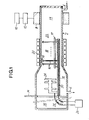
- the device of the invention essentially consists of a quartz tube 2 through which a stream of oxygen passes, the gas penetrating through a nozzle 4 located at one end of the tube and exiting through another tap 6 located at the other end of the tube 2.
- the tube is equipped in the vicinity of its end through which the oxygen arrives with plasma creation means which may consist, for example, of a capacitive electrode 8 connected to a high frequency generator 10 via a tuning box 12.
- plasma creation means which may consist, for example, of a capacitive electrode 8 connected to a high frequency generator 10 via a tuning box 12.
- plasma creation zone there is thus defined at the end of the tube a zone 14 which will be called “plasma creation zone” in the remainder of this text.
- the bodies to be oxidized for example silicon wafers 16 are placed on a support 17 in an area 18 of the tube which is heated by external means, for example an electrical resistance 20.
- these are preferably arranged parallel to each other and perpendicular to the longitudinal axis of the tube.
- the area 18 in which the plates 16 are located is separated from the area 14 excitation of the plasma by an intermediate zone 22 whose length is between 0.5 and 2 times the diameter of the tube 2: the person skilled in the art will determine this distance as a function of each particular case knowing that it must be a direct function of the free path of particles from the tube spraying in the plasma creation area. This ensures the absence of sputtering of the tube and obtain a very good quality of the oxide since the platelets are not likely to be polluted by quartz particles torn from the tube.
- FIG. 1 also shows that the device comprises a cathode 24 placed inside the tube 2 but on the side opposite to the plasma creation zone 14 relative to the central zone 18 where the platelets 16 are located, that is to say ie downstream of the latter with respect to the direction of the oxygen current.
- the cathode 24 is connected by means of a wire 28 to a voltage generator 26 to which the plates 16 are also connected by means of a wire 30 protected by an insulation sheath 32.
- the generator 26 is adjusted in such a way so that the potential of platelets 16 is positive relative to that of cathode 24.
- anode-cathode assembly makes it possible to obtain a higher rate of growth of the oxide.
- the cathode zone is moved away from the plasma creation and excitation zone and when the cathode is placed downstream of the plates to be oxidized with respect to this zone, the polarization field lines of the plates are not disturbed by the intense electric fields prevailing in the plasma creation zone, which ensures perfectly uniform oxide growth over the entire surface of the wafer and on each wafer treated simultaneously if a batch of platelets is treated.
- the wafers are treated in groups of two back to back together, the wafers of a given group being joined at their upper part by staples 38. It is possible with such a device to carry out the oxidation of the wafers either on the two faces, or on only one face while protecting the other with an insulating material.
- the contact between the insulating material and the wafer need not be perfect because, within a few tenths of a millimeter of gap thickness, the plasma cannot penetrate between the wafer and the insulator.
- the oxidation of silicon wafers of a diameter of about 10 cm As a test, the oxidation of silicon wafers of a diameter of about 10 cm. It was found that the best results were obtained by operating at a pressure between 10 and 100 mTorr, preferably between 20 and 50 mTorr and with an oxygen flow rate between 1 and 20 cm 3 / minute.
- the temperature is understood between 300 and 900 ° C and preferably between 500 and 800 ° C.
- the anodization current density that is to say the density of the current passing through the plates, is between 10 and 30 mA / cm 2 for a voltage applied between the anode and the cathode between 50 and 250 volts .
- the plasma excitation frequency it can vary between 0.5 and 30 MHz, the preferred frequency being 13.56 MHz.
- the curves in FIG. 2 represent the oxide thickness obtained as a function of the oxidation time with the device of the invention (curves in solid lines) and with a conventional thermal process (curves in broken lines) on wafers of silicon. It can be seen that by working at 480 ° C with a current density of 10 mA / cm 2 , an oxidation rate is obtained which is higher than that which is obtained at 800 ° C with the thermal process.
- the curve obtained with the device of the invention at 750 ° C with a current density of 30 mA / cm 2 is practically coincident with the curve corresponding to a thermal oxidation carried out at 1000 ° C.
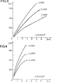
- Figures 3 and 4 show the oxide thickness obtained as a function of the oxidation time for different temperatures, the curves in Figure 3 corresponding to a current density J of 10 mA / cm 2 and Figure 4 corresponding to a current density J of 30 mA / cm 2 .
- Figure 3 shows that after two hours the oxide thickness is of the order of 180 nanometers if we operate at 480 ° C and around 350 nanometers if operating at 770 ° C with a current density of 10 mA / cm 2 .
- FIG. 4 shows that if one operates with a current density of 30 mA / cm 2 , these values pass respectively to 350 and 600 nanometers approximately.
- the device which is the subject of the invention has numerous advantages, the main one of which is to obtain rapid growth of the oxide layer thanks to the fact that the temperature is kept high enough by the external heating, good homogeneity thanks to the fact that the zone where the platelets to be oxidized are located is far from the plasma creation zone and there is no risk of polluting the platelets by the projection of quartz particles torn from the tube in the plasma creation zone.
- High thicknesses can be obtained without electrical breakdowns because the electric field in the oxide is minimized by the possibility offered by the system to carry out anodization at a sufficiently high temperature.
- the invention can be used to locally produce thin dielectric layers on a wafer: it suffices for this to have a mask defining the areas to be treated on the wafer.
- the device described in the present invention is not exclusively applicable to the oxidation of semiconductor materials. It can also be used with virtually no modification to structure, to the nitriding of semiconductor materials. In this case, it suffices to replace the oxygen circulating in the tube with nitrogen, and to reverse the polarizations of the plates and of the cathode (which thus becomes an anode). In the case of use in nitriding, it can be seen that all of the advantages announced for oxidation remain valid. The same furnace comprising the arrangements in accordance with the invention can therefore be used either for oxidation or for nitriding.
Landscapes
- Chemical & Material Sciences (AREA)
- Engineering & Computer Science (AREA)
- Physics & Mathematics (AREA)
- Plasma & Fusion (AREA)
- Analytical Chemistry (AREA)
- General Chemical & Material Sciences (AREA)
- Chemical Kinetics & Catalysis (AREA)
- Materials Engineering (AREA)
- Mechanical Engineering (AREA)
- Metallurgy (AREA)
- Organic Chemistry (AREA)
- Formation Of Insulating Films (AREA)
Applications Claiming Priority (2)
| Application Number | Priority Date | Filing Date | Title |
|---|---|---|---|
| FR8318299A FR2555360B1 (fr) | 1983-11-17 | 1983-11-17 | Dispositif pour la realisation de couches dielectriques minces a la surface de corps solides |
| FR8318299 | 1983-11-17 |
Publications (3)
| Publication Number | Publication Date |
|---|---|
| EP0142450A2 true EP0142450A2 (de) | 1985-05-22 |
| EP0142450A3 EP0142450A3 (de) | 1985-07-10 |
| EP0142450B1 EP0142450B1 (de) | 1988-09-28 |
Family
ID=9294224
Family Applications (1)
| Application Number | Title | Priority Date | Filing Date |
|---|---|---|---|
| EP84402319A Expired EP0142450B1 (de) | 1983-11-17 | 1984-11-14 | Vorrichtung zum Anbringen von dünnen dielektrischen Lagen an Festkörperoberflächen |
Country Status (3)
| Country | Link |
|---|---|
| EP (1) | EP0142450B1 (de) |
| DE (1) | DE3474376D1 (de) |
| FR (1) | FR2555360B1 (de) |
Cited By (2)
| Publication number | Priority date | Publication date | Assignee | Title |
|---|---|---|---|---|
| FR2617333A1 (fr) * | 1987-06-25 | 1988-12-30 | Straboni Alain | Procede d'elimination de zones de nitrure ou d'oxynitrure de silicium |
| FR2630258A1 (fr) * | 1988-04-19 | 1989-10-20 | Straboni Alain | Dispositif de traitement par plasma de plaquettes conductrices |
Family Cites Families (3)
| Publication number | Priority date | Publication date | Assignee | Title |
|---|---|---|---|---|
| US4062747A (en) * | 1976-06-15 | 1977-12-13 | Bell Telephone Laboratories, Incorporated | Native growth of semiconductor oxide layers |
| US4268711A (en) * | 1979-04-26 | 1981-05-19 | Optical Coating Laboratory, Inc. | Method and apparatus for forming films from vapors using a contained plasma source |
| US4323589A (en) * | 1980-05-07 | 1982-04-06 | International Business Machines Corporation | Plasma oxidation |
-
1983
- 1983-11-17 FR FR8318299A patent/FR2555360B1/fr not_active Expired
-
1984
- 1984-11-14 EP EP84402319A patent/EP0142450B1/de not_active Expired
- 1984-11-14 DE DE8484402319T patent/DE3474376D1/de not_active Expired
Cited By (4)
| Publication number | Priority date | Publication date | Assignee | Title |
|---|---|---|---|---|
| FR2617333A1 (fr) * | 1987-06-25 | 1988-12-30 | Straboni Alain | Procede d'elimination de zones de nitrure ou d'oxynitrure de silicium |
| EP0298879A1 (de) * | 1987-06-25 | 1989-01-11 | France Telecom | Verfahren zum Entfernen von Teilen aus Siliciumnitrid oder Siliciumoxynitrid |
| FR2630258A1 (fr) * | 1988-04-19 | 1989-10-20 | Straboni Alain | Dispositif de traitement par plasma de plaquettes conductrices |
| EP0338905A1 (de) * | 1988-04-19 | 1989-10-25 | France Telecom | Vorrichtung zur Plasma-Bearbeitung von leitenden Scheiben |
Also Published As
| Publication number | Publication date |
|---|---|
| EP0142450A3 (de) | 1985-07-10 |
| EP0142450B1 (de) | 1988-09-28 |
| FR2555360A1 (fr) | 1985-05-24 |
| FR2555360B1 (fr) | 1986-10-10 |
| DE3474376D1 (en) | 1988-11-03 |
Similar Documents
| Publication | Publication Date | Title |
|---|---|---|
| EP0801419B1 (de) | Herstellungsverfahren von einem dünnen Halbleiterfilm, der elektronische Anordnungen enthält | |
| JP3329685B2 (ja) | 計測装置および計測方法 | |
| EP0780889B1 (de) | Verfahren zur selektiven Abscheidung von Siliciden hochschmelzender Metalle auf Silizium | |
| WO2003032384A1 (fr) | Procede de fabrication de couches minces contenant des microcomposants | |
| FR2533944A1 (fr) | Procede de fabrication d'articles par depot en phase vapeur d'une matiere a constituants multiples | |
| FR3085538A1 (fr) | Tranche soi et son procede de production | |
| EP0263788A1 (de) | Verfahren und Vorrichtung zum Auftragen von hydriertem, amorphem Silizium auf ein Substrat in Plasmaumgebung | |
| WO2020008116A1 (fr) | Substrat pour un dispositif integre radioafrequence et son procede de fabrication | |
| FR2542500A1 (fr) | Procede de fabrication d'un dispositif semiconducteur du type comprenant au moins une couche de silicium deposee sur un substrat isolant | |
| FR2984007A1 (fr) | Procede de stabilisation d'une interface de collage situee au sein d'une structure comprenant une couche d'oxyde enterree et structure obtenue | |
| FR2551244A1 (fr) | Procede de fabrication d'un substrat pour dispositif a commande electrique et ecran de visualisation elabore a partir d'un tel substrat | |
| EP0142450B1 (de) | Vorrichtung zum Anbringen von dünnen dielektrischen Lagen an Festkörperoberflächen | |
| EP0900859B1 (de) | Verfahren zur Ablagerung einer dielektrischen Ta2O5-Schicht | |
| FR3029352A1 (fr) | Procede d'assemblage de deux substrats | |
| Nunomura et al. | Ion bombardment-induced defect reduction at a-Si: H/c-Si interfaces: possible microstructural changes and mobile hydrogen roles | |
| FR2987935A1 (fr) | Procede d'amincissement de la couche active de silicium d'un substrat du type "silicium sur isolant" (soi). | |
| CH620314A5 (en) | Method and apparatus for chemical treatment in a luminescent discharge | |
| FR3040529B1 (fr) | Procede de fabrication d'une tranche soi et tranche soi | |
| EP2035597B1 (de) | Reinigungsvorrichtung und reinigungsverfahren für einen plasmareaktor | |
| FR2529384A1 (fr) | Procede de reduction de compose en couche sur un substrat et son application a la fabrication de structure semi-conductrice a effet de champ | |
| FR2734284A1 (fr) | Dispositif de traitement chimique superficiel d'un echantillon plat au moyen d'un gaz actif | |
| FR2930674A1 (fr) | Procede de traitement d'une heterostructure comportant une couche mince en materiau ferroelectrique | |
| JPH101772A (ja) | ウェハートレーと真空装置、及び熱電性ウェハーの真空処理方法 | |
| EP0338905B1 (de) | Vorrichtung zur Plasma-Bearbeitung von leitenden Scheiben | |
| EP1566468A2 (de) | Verfahren zur Herstellung von integrierten Schaltungen und entsprechende Vorrichtung |
Legal Events
| Date | Code | Title | Description |
|---|---|---|---|
| PUAI | Public reference made under article 153(3) epc to a published international application that has entered the european phase |
Free format text: ORIGINAL CODE: 0009012 |
|
| PUAL | Search report despatched |
Free format text: ORIGINAL CODE: 0009013 |
|
| AK | Designated contracting states |
Designated state(s): DE GB IT NL |
|
| AK | Designated contracting states |
Designated state(s): DE GB IT NL |
|
| RTI1 | Title (correction) | ||
| 17P | Request for examination filed |
Effective date: 19851212 |
|
| 17Q | First examination report despatched |
Effective date: 19870702 |
|
| GRAA | (expected) grant |
Free format text: ORIGINAL CODE: 0009210 |
|
| AK | Designated contracting states |
Kind code of ref document: B1 Designated state(s): DE GB IT NL |
|
| GBT | Gb: translation of ep patent filed (gb section 77(6)(a)/1977) | ||
| ITF | It: translation for a ep patent filed | ||
| REF | Corresponds to: |
Ref document number: 3474376 Country of ref document: DE Date of ref document: 19881103 |
|
| PLBE | No opposition filed within time limit |
Free format text: ORIGINAL CODE: 0009261 |
|
| STAA | Information on the status of an ep patent application or granted ep patent |
Free format text: STATUS: NO OPPOSITION FILED WITHIN TIME LIMIT |
|
| 26N | No opposition filed | ||
| ITTA | It: last paid annual fee | ||
| PGFP | Annual fee paid to national office [announced via postgrant information from national office to epo] |
Ref country code: GB Payment date: 19961106 Year of fee payment: 13 |
|
| PGFP | Annual fee paid to national office [announced via postgrant information from national office to epo] |
Ref country code: DE Payment date: 19961122 Year of fee payment: 13 |
|
| PGFP | Annual fee paid to national office [announced via postgrant information from national office to epo] |
Ref country code: NL Payment date: 19961128 Year of fee payment: 13 |
|
| PG25 | Lapsed in a contracting state [announced via postgrant information from national office to epo] |
Ref country code: GB Free format text: LAPSE BECAUSE OF NON-PAYMENT OF DUE FEES Effective date: 19971114 |
|
| PG25 | Lapsed in a contracting state [announced via postgrant information from national office to epo] |
Ref country code: NL Free format text: LAPSE BECAUSE OF NON-PAYMENT OF DUE FEES Effective date: 19980601 |
|
| GBPC | Gb: european patent ceased through non-payment of renewal fee |
Effective date: 19971114 |
|
| PG25 | Lapsed in a contracting state [announced via postgrant information from national office to epo] |
Ref country code: DE Free format text: LAPSE BECAUSE OF NON-PAYMENT OF DUE FEES Effective date: 19980801 |
|
| NLV4 | Nl: lapsed or anulled due to non-payment of the annual fee |
Effective date: 19980601 |