EP0142520B1 - Schaltung zur realisierung verbesserter anstiegsgeschwindigkeit von operationsverstärkern - Google Patents
Schaltung zur realisierung verbesserter anstiegsgeschwindigkeit von operationsverstärkern Download PDFInfo
- Publication number
- EP0142520B1 EP0142520B1 EP84901560A EP84901560A EP0142520B1 EP 0142520 B1 EP0142520 B1 EP 0142520B1 EP 84901560 A EP84901560 A EP 84901560A EP 84901560 A EP84901560 A EP 84901560A EP 0142520 B1 EP0142520 B1 EP 0142520B1
- Authority
- EP
- European Patent Office
- Prior art keywords
- capacitor
- output
- voltage
- circuit
- level
- Prior art date
- Legal status (The legal status is an assumption and is not a legal conclusion. Google has not performed a legal analysis and makes no representation as to the accuracy of the status listed.)
- Expired
Links
- 239000003990 capacitor Substances 0.000 claims abstract description 101
- 230000006641 stabilisation Effects 0.000 abstract description 8
- 238000011105 stabilization Methods 0.000 abstract description 8
- 230000006872 improvement Effects 0.000 abstract description 6
- 230000000694 effects Effects 0.000 abstract description 3
- 101150052012 PPP1R14B gene Proteins 0.000 abstract 1
- 101100013829 Zea mays PHI1 gene Proteins 0.000 abstract 1
- 238000010586 diagram Methods 0.000 description 6
- 230000008859 change Effects 0.000 description 2
- 230000005669 field effect Effects 0.000 description 2
- 230000004048 modification Effects 0.000 description 2
- 238000012986 modification Methods 0.000 description 2
- 230000009467 reduction Effects 0.000 description 2
- 230000008901 benefit Effects 0.000 description 1
- 238000002955 isolation Methods 0.000 description 1
- 229910044991 metal oxide Inorganic materials 0.000 description 1
- 150000004706 metal oxides Chemical class 0.000 description 1
- 230000000717 retained effect Effects 0.000 description 1
- 238000005070 sampling Methods 0.000 description 1
- 239000004065 semiconductor Substances 0.000 description 1
- 239000000758 substrate Substances 0.000 description 1
- 230000007704 transition Effects 0.000 description 1
Images

Classifications
-
- H—ELECTRICITY
- H03—ELECTRONIC CIRCUITRY
- H03F—AMPLIFIERS
- H03F1/00—Details of amplifiers with only discharge tubes, only semiconductor devices or only unspecified devices as amplifying elements
- H03F1/08—Modifications of amplifiers to reduce detrimental influences of internal impedances of amplifying elements
- H03F1/083—Modifications of amplifiers to reduce detrimental influences of internal impedances of amplifying elements in transistor amplifiers
- H03F1/086—Modifications of amplifiers to reduce detrimental influences of internal impedances of amplifying elements in transistor amplifiers with FET's
-
- G—PHYSICS
- G11—INFORMATION STORAGE
- G11C—STATIC STORES
- G11C27/00—Electric analogue stores, e.g. for storing instantaneous values
- G11C27/02—Sample-and-hold arrangements
- G11C27/024—Sample-and-hold arrangements using a capacitive memory element
- G11C27/026—Sample-and-hold arrangements using a capacitive memory element associated with an amplifier
Definitions
- This invention relates to the design of operational amplifiers and, in particular, to the design of the output stage of operational amplifiers intended to provide an output voltage which switches (or alternates) between a first output reference voltage and a second output signal voltage level.
- the signal voltage may be time varying.
- the rate at which the output voltage of an operational amplifier changes from a first level to a second level during the slewing time interval is called the slew rate dV/dt.
- the slew rate is limited to a maximum value determined by the input stage bias current 1 1 and the size of the internal stabilization capacitor (Cs).
- the first voltage level may be a reference level such as ground or the offset voltage of the differential input stage of the operational amplifier.
- the second voltage level may be a specific time varying voltage level which .
- the operational amplifier is required to provide at its output.
- an operational amplifier comprising an output stage amplifier having an input terminal and an output terminal, and a. first capacitor between said input terminal and said output terminal characterised by:
- the amplifier may be controlled to operate alternately in each of two modes.
- the output of the operational amplifier In the first mode, the output of the operational amplifier is reset to a reference signal or ground.
- the output .of the operational amplifier samples the level of a time varying second voltage signal.
- the improvement consists of replacing the stabilization capacitor of prior art output circuits with a pair of stabilization capacitors connected in parallel.
- a series connected switch is associated with each capacitor for switching the associated capacitor into and out of the circuit. The switches are operated by a respective one of a pair of external non-overlapping clock pulse trains so as to not be closed simultaneously.
- the effect of this improved output circuit is to allow the output voltage of the operational amplifier to snap up to the last previous level of a sampled input voltage at a rate which is not restricted by the first stage slew rate limit.
- slewing begins at a higher rate, limited only by the output stage slew rate capability.
- the slew interval will therefore consume less time. Because the time interval during which the output slews is greatly reduced, the output has more time to settle and track the time varying voltage than in prior art devices.
- the output of the operational amplifier thus shows greater correlation with the level of the second or time varying signal:
- FIG. 1 The environment in which the circuit of the present invention is intended to operate is typified by the circuit shown in FIG. 1.
- That circuit is simplified circuit diagram of an insulated gate field effect transistor (IGFET) circuit formed on a semi-conductive substrate for performing a sample and reset function.
- IGFET insulated gate field effect transistor
- This circuit is the subject of a copending patent application of Lucas et al, Serial No. 316,453 (US-A-4439693), filed October 30,1981, titled "Sample and Hold Circuit with Improved Offset Compensation". That application is assigned to the same assignee as is the present application.
- a detailed explanation of the circuit of FIG. 1 may be found in the referenced copending application. Only an abbreviated explanation will be given herein.
- the switch 50 permits alternate connection of the input capacitor 40 to the input voltage source 18 and ground.
- the switch 52 permits the alternate connection of the amplifier output 10c to the amplifier inverting input 10b and to plate 42b of the feedback capacitor 42.
- the switch 54 permits connection of the feedback capacitor plate 42b to ground.
- the switch 56 is operated during the "sample” mode to disconnect the positive amplifier input 10a from ground leaving the positive amplifier input connected to the capacitors 60 and 62.
- the value of capacitors 60 and 62 are selected to be proportional to the value of capacitors 40 and 42, respectively.
- the purpose of the capacitors 60, 62 is to provide compensation for the leakage cur- rents I ln- and I ln+ which leak through the switches 56 and 52, respectively, during the "sample” mode.
- each of the switches 52, 56 is formed as a metal oxide semiconductor field effect transistor (MOSFET).
- MOSFET metal oxide semiconductor field effect transistor
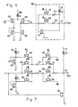
- the circuit of FIG. 2 comprises a first current source 100, a pair of P-type FETs 102, 104 forming the differential input, a pair of N-type FETs 106, 108 forming a current mirror, and an output stage 109 comprising a second current source 110, an N-type FET 112 and a stabilization capacitor 113.
- the inverting input terminal 114 and the positive input terminal 116 correspond respectively to the input terminals 10b and 10a of op amp 10 of FIG. 1.
- Output terminal 118 provides the output signal and corresponds to terminal 10c of FIG. 1.
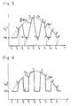
- the circuit of FIG. 1 may be operated in a sample and reset mode to give the output waveform V out a shown in FIG. 3 when the input waveform is sinusoidal such as V in .
- V ref typically the offset voltage of the op amp.
- V out is at V ref for the time interval t 1 to t 2 .
- the output V out ideally should track V in .
- V out can rise only at the maximum slew rate dV/dt set by the input stage bias current I 1 from source 100 and the size of the stabilization capacitor 113 (Cs).
- the maximum rate dV/dt max is expressed as I 1 / Cs and is commonly referred to as the input stage slew rate limit.
- V out will rise at this maximum slew rate until it nears V ln as indicated at A in FIG. 3. Thereafter, V out will settle toward V ln until the time t 3 . At time t 3 , V out would ideally switch to V ref and remain there until t 4 . However, V out can only slew toward V ref at a rate of -dV/dt max .
- V out thus begins the slew downward towards V ref and continues to slew at the maximum rate until it reaches point B where it begins to settle into the level V ref .
- the time period between B and C is referred to as the settling time of the waveform V out .
- the output V out tracks V ref .
- the switching circuitry again places the circuit of FIG. 1 in the sample mode.
- V out thus begins to rise at the rate dV/dt max. Since V ln has now reached a higher level, V out must slew for a longer time period, i.e., slews from t 4 to point D. This time span is significantly longer than the time span t 2 to point A. Because it takes so long to approach the level of V ln , V out cannot reach V ln during the period D to E.
- V out actually tracks V ln only for the time span from point H to point I.
- the lower level of V ln permits V out to track for a relatively long period of time between point L and tg.
- the higher the voltage level of V ln the longer is the slew time, and the less time there is available to actually settle to and track the desired voltage V ln or V ref .
- the present invention is a switching circuit intended to modify the output stage 109 of the circuit of FIG. 2. On the average, the invention reduces the time required to slew to the level of V ln , thereby leaving a greater portion of the sample or reset periods available for actually tracking either the input voltage V ln , or the reference voltage V,f, as appropriate.
- the modification to the circuit is illustrated by the output stage 109' of FIG. 4.
- the disadvantages of the circuit of FIG. 2 stem from the fact that a single capacitor is required to switch between both the reference level V ref and the input signal V, n . Before the single capacitor 113 can track one signal, it must charge or discharge from the voltage retained when tracking the other signal. In the improved circuit of FIG. 4, one capacitor, e.g., 123, is dedicated to tracking V ln and another capacitor, e.g., 125, is dedicated to tracking the other voltage level V ref . Thus, neither capacitor is required to track both V out and V ref , each is free to retain the last achieved voltage level of the signal which it tracks.
- the improvement of the invention comprises replacing capacitor 113 of FIG. 2 by a pair of capacitors 123 and 125, each of which may be selectively switched in or out of the tracking mode by a respective switch means such as switches 127 and 129 which may comprise a pair of FET switches.
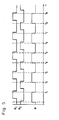
- the switches 127 and 129 are operated such that they are never both closed at the same time. This is accomplished by the pair of nonoverlapping clock signals ⁇ 1 and ⁇ 2 shown in FIG. 5.
- ⁇ 1 could be used to control switch 127. When ⁇ 1 is high, switch 127 would be closed thereby placing capacitor 123 in the circuit to track the input signal. When ⁇ 1 is high, ⁇ 2 is low and switch 129 is open.
- capacitor 125 would be out of the circuit and would retain or "hold” the voltage level that it had reached during the last time it was in the circuit (i.e., when switch 129 was closed).
- ⁇ 1 and ⁇ 2 must be operated in synchronism with the signal ⁇ of the circuit of FIG. 1.
- ⁇ goes to its high state for the period t 2 to t 3 of FIG. 5.
- This connects capacitor 40 to the input voltage V ln and connects output terminal 10c to plate 42b of capacitor 42.
- Switches 54 and 56 are opened.
- This is the "sample" mode of the circuit of FIG. 1.
- ⁇ 1 is high, causing switch 127 to be closed, thus switching capacitor 123 into circuit.
- ⁇ 2 is low causing switch 129 to be open, thus switching capacitor 125 out of the circuit where it will retain the voltage level V ref .
- capacitor 123 is switched into the circuit, the voltage stored across it will be nearly the same as reached during the previous sample period which ended at t i .
- Capacitor 123 then begins to charge or discharge towards the current value of V ln .
- the capacitor 123 can change voltage only at a maximum rate dV/dt equal to the slew rate I 1 / Cs1 where CS1 is the value of capacitor 123.
- the output voltage begins to rise at the input stage limited slew rate and at point A of FIG. 6 nears V, " and thereafter settles into and tracks V, n .
- ⁇ changes to its low state for the time period t 3 to t 4 .
- This connects capacitor 40 - of FIG. 1 to the ground and connects the output terminal 10c to the inverting input terminal 10b.
- Switches 54 and 56 are closed.
- ⁇ 1 is low causing switch 127 to be open, thus removing capacitor 123 from the circuit.
- Capacitor 123 while removed during this period t 3 to t 4 , will retain the last voltage level which it had reached, i.e., the voltage at just prior to time t 3 .
- ⁇ 1 is low, ⁇ 2 is high, causing switch 129 to close and switch capacitor 125 into the circuit.
- V out When capacitor 125 is switched into the circuit, the output voltage V out slews at a high rate, limited only by the output stage slew rate, not the input stage slew rate. It then settles to the value of the voltage previously stored in capacitor 125, which is V ref . Thus, V out is not required to slew back to V ref at a rate determined by the input stage slew rate limit as was the case in FIG. 3 for the time period t 3 to point B. V out will thus accurately rack V ref for most of the period t 3 to t 4 .
- ⁇ changes from low to its high state and stays in its high state for the period t 4 to t s .
- This again connects capacitor 40 to the input voltage V ln and connects output terminal 10c to plate 42b of capacitor 42.
- Switches 54 and 56 are closed.
- ⁇ 1 goes to high closing switch 127 and switching capacitor 123 into the circuit.
- ⁇ 2 is now low, switching capacitor 125 out of the circuit, where it retains its level V ret .
- capacitor 123 is switched into the circuit, it still has stored on it the last voltage level reached during the previous sample period, t 2 to t 3 .
- V out slews at a high rate, limited only by the output stage slew rate, not the input stage slew rate, from V ref to the value previously stored on capacitor 123, i.e., the high voltage level shown in FIG. 6 at time t 3 .
- V out thus begins to rise at the output stage slew rate limit until at point D it nears the level of, and begins to settle toward, V ln .
- the time duration required to slew to near the level of V ln i.e., the time t 4 to point D, is significantly less than the corresponding slew time required by the circuit of FIG. 2, which time is shown as the period t 4 to D in FIG. 3.
- V out the time that V out settles to and tracks V ln is much greater in FIG. 6 (i.e., point D to E) than in FIG. 3 (point D to E). Note that in FIG. 3, because of the slew rate limitation, V out never reaches V ln during the t 4 to t 5 interval.
- V out begins at V ref and slews at a rapid rate toward the previously stored value of V ln . It may go above the value of V ln and slews back down toward V ln at the rate of ⁇ Is1/Cs1 until it gets relatively close to V ln and then gradually settles into and tracks V ln as at points H and L.
- the output waveform shown in FIG. 6 can readily be compared to the output waveform of FIG. 3. It is apparent that V out of FIG.
- V out of FIG. 6 tracks the desired voltage levels V ref and V ln for a greater percentage of the time period t 1 to tg than does V out of FIG. 3. - V out of FIG. 6 is required to slew from one voltage level to another for much less time than required in FIG. 3. Although the input slew rate limit dV/dt is the same for the circuits of FIG. 2 and FIG. 4, the output V out of FIG. 6 requires less time for slewing.
- the slewing time of the circuit of FIG. 4 will generally be less than the slewing time of the circuit of FIG. 2.
- the output V out will thus show greater correlation with V ln for the circuit of FIG. 4 than was achieved by the circuit of FIG. 2.
- the improvement in slewing time may be computed as follows:
- Vd the voltage difference between the reference voltage level V ref and the voltage level of the desired output voltage waveform V ln . Then: where dV/dtmax has been previously defined as the maximum slewing rate sized by I 1 /Cs.
- Tsn Let the input stage limited slewing time of the new and improved circuit be designated Tsn. Let ⁇ V out be the maximum voltage through which the new circuit must slew at the input stage limited slew rate dV/dt max . Assume (see FIG. 6) that the time required to slew, at the output stage limited slew rate, to the previously stored voltage is small in comparison to Tsn. Then:
- ⁇ V out represents the difference between signal output voltage levels occurring over the time interval in which the reference voltage is present at the amplifier output. This time interval is usually T clk /2 where T clk is the clock period (i.e., the period of the externally supplied clock pulse train).
- the clock frequency f c is usually several times (e.g., usually 10 times) the mid band frequency f s .
- the improvement factor is 10/n or about a factor of 3 reduction in slewing time.
- This reduction in slewing time can be used to great advantage.
- the reduced slewing time typically permits the same amplifier to be used at more than double the clock rate. That is, a circuit using the present invention can utilize values for n which are twice that of the old circuit and thereby significantly reduce distortion produced by sampling as in switched capacitor filter circuit applications. Similarly, equivalent results can be obtained by the new circuit even if the current limited slew rate, and therefore the power supplied to the operational amplifier, is reduced by about 50%.
- the three factors, tracking capability, clock rate and power consumption can be balanced against one another and traded off to achieve the most desired output waveform characteristics.
- FIG. 7 An alternate embodiment of the invention is shown in FIG. 7.
- the alternate embodiment is a more versatile version of the circuit of FIG. 4.
- the increased versatility is achieved by adding switching devices such as switches 137 and 139 on the other side of the respective capacitors 123 and 125. This permits complete isolation of capacitors 123 and 125 from the remainder of the circuit.
- switch devices 130 and 132 and properly biasing FET 134 capacitor 123 may be precharged to a selected voltage level while capacitor s125 is switched into the circuit.
- switch devices 136 and 138 and properly biasing FET 140 capacitor 125 may be precharged to a selected voltage level while capacitor 123 is switched into the circuit.
- the added switches 137,132 and 130, and the biasing FET 134 may be referred to generally as a precharging means for capacitor 123.
- the output voltage V out may be caused to return to any desired voltage level whenever the non-overlapping clock signals change state.
- V out can be caused to slew rapidly toward a reference level other than the last stored value of V ref (shown in FIG. 6) during the "reset" period such as t 3 to t 4 , and V out may also be caused to slew rapidly to any predetermined level, independent of the last sampled value of V out , as was the case at times t 4 to t s when the sample period begins.
- capacitor 123 is switched out of the circuit and into the precharge configuration.
- Capacitor 125 precharges through switches 136 and 138 to ground (or another predetermined reference).
- ⁇ 1 is low and ⁇ 2 is high
- capacitor 123 is switched out of the circuit and into the precharge mode while capacitor 125 is switched into the circuit.
- the circuit of FIG. 7 can easily be operated to perform identically to the circuit of FIG. 4. This is accomplished by not applying any clock signal ⁇ 1 or IP2 to switches 130,132,138, which thus remain open, and driving switches 137 and 139 with a voltage which will keep the switches constantly closed. The configuration of the circuit of FIG. 7 then becomes electrically equivalent to the circuit of FIG. 4. ⁇
- FIGS. 4 through 7 the figures are for purposes of illustration only and should not be interpreted in a limiting sense.
- the non-overlapping clock pulse trains could also be-a single clock pulse train, the high level of which would serve to close those switches driven by ⁇ 1 and open those switches driven by ⁇ 2 .
- This could be accomplished by appropriate selection of FETs as either P-type or N-type as required.
- the signal ⁇ used to select the operating mode of the circuit of FIG. 1 could be used to serve the function of the non-overlapping pulse trains ⁇ 1 and ⁇ 2 .
Landscapes
- Engineering & Computer Science (AREA)
- Power Engineering (AREA)
- Amplifiers (AREA)
Claims (3)
Applications Claiming Priority (2)
| Application Number | Priority Date | Filing Date | Title |
|---|---|---|---|
| US486644 | 1983-04-20 | ||
| US06/486,644 US4500846A (en) | 1983-04-20 | 1983-04-20 | Circuit for effecting improved slew rate of operational amplifiers |
Publications (2)
| Publication Number | Publication Date |
|---|---|
| EP0142520A1 EP0142520A1 (de) | 1985-05-29 |
| EP0142520B1 true EP0142520B1 (de) | 1987-12-02 |
Family
ID=23932703
Family Applications (1)
| Application Number | Title | Priority Date | Filing Date |
|---|---|---|---|
| EP84901560A Expired EP0142520B1 (de) | 1983-04-20 | 1984-04-06 | Schaltung zur realisierung verbesserter anstiegsgeschwindigkeit von operationsverstärkern |
Country Status (5)
| Country | Link |
|---|---|
| US (1) | US4500846A (de) |
| EP (1) | EP0142520B1 (de) |
| JP (1) | JPS60501085A (de) |
| DE (1) | DE3467948D1 (de) |
| WO (1) | WO1984004421A1 (de) |
Families Citing this family (10)
| Publication number | Priority date | Publication date | Assignee | Title |
|---|---|---|---|---|
| DE69529828D1 (de) * | 1995-11-30 | 2003-04-10 | St Microelectronics Srl | Operationsverstärker mit steuerbarer Frequenzkompensation |
| EP0836275B1 (de) * | 1996-10-11 | 2002-06-05 | STMicroelectronics S.r.l. | Schneller geschalteter Operationsverstärker für Anwendungen bei niedriger Versorgungsspannung |
| US5877654A (en) * | 1996-12-02 | 1999-03-02 | Motorola Inc. | Class a amplifier with a digitally programmable miller compensation network |
| DE10031522B9 (de) * | 2000-06-28 | 2007-07-12 | Infineon Technologies Ag | Frequenzkompensierte Verstärkeranordnung und Verfahren zum Betrieb einer frequenzkompensierten Verstärkeranordnung |
| US7068098B1 (en) | 2002-11-25 | 2006-06-27 | National Semiconductor Corporation | Slew rate enhancement circuit |
| US7605854B2 (en) * | 2004-08-11 | 2009-10-20 | Broadcom Corporation | Operational amplifier for an active pixel sensor |
| KR100699829B1 (ko) | 2004-12-09 | 2007-03-27 | 삼성전자주식회사 | 높은 슬루 레이트를 가지는 액정 표시 장치에 포함된 소스드라이버의 출력 버퍼 및 출력 버퍼의 제어 방법 |
| DE102007048454B3 (de) * | 2007-10-10 | 2009-03-19 | Texas Instruments Deutschland Gmbh | Schaltkreis zur Kompensation von leckstrominduziertem Offset in einem asymmetrischen Operationsverstärker |
| TWI427920B (zh) * | 2010-02-01 | 2014-02-21 | Novatek Microelectronics Corp | 耦合阻絕方法及運算放大器 |
| CN119311067B (zh) * | 2024-12-18 | 2025-03-21 | 上海灵动微电子股份有限公司 | 一种电压调整电路、电源电路、集成电路以及电子设备 |
-
1983
- 1983-04-20 US US06/486,644 patent/US4500846A/en not_active Expired - Lifetime
-
1984
- 1984-04-06 WO PCT/US1984/000495 patent/WO1984004421A1/en not_active Ceased
- 1984-04-06 DE DE8484901560T patent/DE3467948D1/de not_active Expired
- 1984-04-06 EP EP84901560A patent/EP0142520B1/de not_active Expired
- 1984-04-06 JP JP59501544A patent/JPS60501085A/ja active Pending
Also Published As
| Publication number | Publication date |
|---|---|
| DE3467948D1 (en) | 1988-01-14 |
| EP0142520A1 (de) | 1985-05-29 |
| JPS60501085A (ja) | 1985-07-11 |
| US4500846A (en) | 1985-02-19 |
| WO1984004421A1 (en) | 1984-11-08 |
Similar Documents
| Publication | Publication Date | Title |
|---|---|---|
| US6323697B1 (en) | Low distortion sample and hold circuit | |
| US5084634A (en) | Dynamic input sampling switch for CDACS | |
| EP0060026B1 (de) | Verstärkerstufe mit Operationsverstärker und äquivalentem Widerstandsschaltkreis mit schaltbaren Kapazitäten | |
| US5376841A (en) | Sample-and-hold circuit device | |
| US3819954A (en) | Signal level shift compensation in chargetransfer delay line circuits | |
| US20030042936A1 (en) | Gate bootstrapped cmos sample-and-hold circuit | |
| US4344050A (en) | Dual channel digitally switched capacitor filter | |
| EP0142520B1 (de) | Schaltung zur realisierung verbesserter anstiegsgeschwindigkeit von operationsverstärkern | |
| US20020167343A1 (en) | Pre-charged sample and hold | |
| US4255715A (en) | Offset correction circuit for differential amplifiers | |
| JP2762868B2 (ja) | 電圧比較回路 | |
| US5130571A (en) | Optimizing speed and charge injection parameters of a switched capacitor circuit | |
| US4237390A (en) | Switching comparator | |
| US5148054A (en) | High accuracy MOSFET-switched sampling circuit | |
| EP0015554B1 (de) | Vergleichsschaltung | |
| US3982196A (en) | Differential voltage amplifier | |
| JP2591066B2 (ja) | アナログスイッチ回路 | |
| JP2000223969A (ja) | 高速サンプルホ―ルド回路用の低電圧バッファ増幅器 | |
| US3983409A (en) | Bucket-brigade circuit | |
| GB2157108A (en) | Eliminating input offset | |
| JPS63148173A (ja) | チヨツパ型比較器 | |
| US4254345A (en) | Output circuit for bucket-brigade devices | |
| US4616145A (en) | Adjustable CMOS hysteresis limiter | |
| EP0669718A1 (de) | Elektronischer Schalter für integrierte MOS-Schaltungen mit niedriger Versorgungsspannung | |
| JP2000132989A (ja) | トラックホールド回路 |
Legal Events
| Date | Code | Title | Description |
|---|---|---|---|
| PUAI | Public reference made under article 153(3) epc to a published international application that has entered the european phase |
Free format text: ORIGINAL CODE: 0009012 |
|
| 17P | Request for examination filed |
Effective date: 19841217 |
|
| AK | Designated contracting states |
Designated state(s): DE FR GB |
|
| 17Q | First examination report despatched |
Effective date: 19860417 |
|
| RAP1 | Party data changed (applicant data changed or rights of an application transferred) |
Owner name: HUGHES AIRCRAFT COMPANY |
|
| GRAA | (expected) grant |
Free format text: ORIGINAL CODE: 0009210 |
|
| AK | Designated contracting states |
Kind code of ref document: B1 Designated state(s): DE FR GB |
|
| REF | Corresponds to: |
Ref document number: 3467948 Country of ref document: DE Date of ref document: 19880114 |
|
| ET | Fr: translation filed | ||
| PLBE | No opposition filed within time limit |
Free format text: ORIGINAL CODE: 0009261 |
|
| STAA | Information on the status of an ep patent application or granted ep patent |
Free format text: STATUS: NO OPPOSITION FILED WITHIN TIME LIMIT |
|
| 26N | No opposition filed | ||
| PGFP | Annual fee paid to national office [announced via postgrant information from national office to epo] |
Ref country code: FR Payment date: 19910313 Year of fee payment: 8 |
|
| PGFP | Annual fee paid to national office [announced via postgrant information from national office to epo] |
Ref country code: GB Payment date: 19910315 Year of fee payment: 8 |
|
| PGFP | Annual fee paid to national office [announced via postgrant information from national office to epo] |
Ref country code: DE Payment date: 19910402 Year of fee payment: 8 |
|
| PG25 | Lapsed in a contracting state [announced via postgrant information from national office to epo] |
Ref country code: GB Effective date: 19920406 |
|
| GBPC | Gb: european patent ceased through non-payment of renewal fee | ||
| PG25 | Lapsed in a contracting state [announced via postgrant information from national office to epo] |
Ref country code: FR Effective date: 19921230 |
|
| PG25 | Lapsed in a contracting state [announced via postgrant information from national office to epo] |
Ref country code: DE Effective date: 19930101 |
|
| REG | Reference to a national code |
Ref country code: FR Ref legal event code: ST |