EP0142579A1 - Aufzeichnungsgerät - Google Patents
Aufzeichnungsgerät Download PDFInfo
- Publication number
- EP0142579A1 EP0142579A1 EP83201561A EP83201561A EP0142579A1 EP 0142579 A1 EP0142579 A1 EP 0142579A1 EP 83201561 A EP83201561 A EP 83201561A EP 83201561 A EP83201561 A EP 83201561A EP 0142579 A1 EP0142579 A1 EP 0142579A1
- Authority
- EP
- European Patent Office
- Prior art keywords
- photoreceptor
- radiation sources
- row
- line
- rows
- Prior art date
- Legal status (The legal status is an assumption and is not a legal conclusion. Google has not performed a legal analysis and makes no representation as to the accuracy of the status listed.)
- Granted
Links
Images


Classifications
-
- H—ELECTRICITY
- H04—ELECTRIC COMMUNICATION TECHNIQUE
- H04N—PICTORIAL COMMUNICATION, e.g. TELEVISION
- H04N1/00—Scanning, transmission or reproduction of documents or the like, e.g. facsimile transmission; Details thereof
- H04N1/04—Scanning arrangements, i.e. arrangements for the displacement of active reading or reproducing elements relative to the original or reproducing medium, or vice versa
- H04N1/19—Scanning arrangements, i.e. arrangements for the displacement of active reading or reproducing elements relative to the original or reproducing medium, or vice versa using multi-element arrays
- H04N1/191—Scanning arrangements, i.e. arrangements for the displacement of active reading or reproducing elements relative to the original or reproducing medium, or vice versa using multi-element arrays the array comprising a one-dimensional [1D] array
- H04N1/1911—Simultaneously or substantially simultaneously scanning picture elements on more than one main scanning line, e.g. scanning in swaths
- H04N1/1913—Scanning adjacent picture elements in different scans of the array, e.g. in complementary checkerboard patterns
-
- H—ELECTRICITY
- H04—ELECTRIC COMMUNICATION TECHNIQUE
- H04N—PICTORIAL COMMUNICATION, e.g. TELEVISION
- H04N1/00—Scanning, transmission or reproduction of documents or the like, e.g. facsimile transmission; Details thereof
- H04N1/04—Scanning arrangements, i.e. arrangements for the displacement of active reading or reproducing elements relative to the original or reproducing medium, or vice versa
- H04N1/19—Scanning arrangements, i.e. arrangements for the displacement of active reading or reproducing elements relative to the original or reproducing medium, or vice versa using multi-element arrays
- H04N1/195—Scanning arrangements, i.e. arrangements for the displacement of active reading or reproducing elements relative to the original or reproducing medium, or vice versa using multi-element arrays the array comprising a two-dimensional [2D] array
- H04N1/19505—Scanning picture elements spaced apart from one another in at least one direction
- H04N1/1951—Scanning picture elements spaced apart from one another in at least one direction in one direction
Definitions
- the present invention relates to a recording apparatus for linewise recording information upon a moving photoreceptor.
- Apparatus for recording information upon a moving photoreceptor comprising a multiplicity of stationary pointlike radiation sources that are distributed along a recording head extending transversely of the direction of displacement of a photoreceptor, and that are individually energizable for information-wise exposing the photoreceptor in response to received information signals as the photoreceptor moves past the recording head.
- the transfer of the images of the radiation sources onto the photoreceptor can be achieved by means of lens arrangements, fiber optics or fiber pipes, self focussing fibers, or the like.
- the recording head prefferably comprises two parallel staggered rows of the radiation sources. In comparison with the use of a single row of radiation sources the spacing between adjacent sources of a row can in those circumstances be doubled while achieving the same image resolution.
- a recording head comprising at least about 2200 discrete radiation sources is required.
- a plurality of light sources in the form of LED's (light-emitting diodes) can be formed as an array on a monolithic semi-conductor chip. By line-wise assembling a plurality of chips, a recording head having a length of 216 m can be obtained.
- the illumination of the sources forming the more downstream row, reckoning in the direction of motion of the photoreceptor must be delayed relative to the illumination of the sources of the other row in order that the projected images of the different rows of sources shall be on a common transverse line across the photoreceptor.
- Apparatus wherein such a delay occurs are disclosed e.g. in GB Appl. 2,042,746 A of Savin Corporation, relating to a multiple variable light source photographic printer, and in European Appl. 82 201 324.9 of Agfa-Gevaert N.V., relating to a recording apparatus.
- Recording apparatus is of a kind known per se, comprising a recording head with a multiplicity of individually addressable and energisable point-like radiation sources arranged in staggered parallel rows for irradiating points across a photoreceptor during movement thereof relative to and in a direction normal to said rows, and driver circuits for simultaneously energising the radiation sources of each row responsive to respective data bit input signals serially applied to said driver circuits during an information line period, there being delay means for delaying energisation of the radiation sources of a first said row relative to the energisation of the sources of a second said row thereby to compensate for the distance between such rows.
- the apparatus according to the invention is distinguished from the known apparatus of that kind by the following combination of characterising features :
- line period stands in the present specification for the period of time which equals 1 s, wherein n is the number of lines recorded per second.
- the recording head of an apparatus may include more than two staggered rows of said point-like radiation sources.
- delay means for delaying energisation of the radiation sources of said second row relative to those of the third row, and so on if there are more than three rows.
- trigger means responsive to signals from the photoreceptor speed monitoring means for triggering the commencement of the energisation period of the radiation sources of the third and any subsequent row to ensure transverse alignment of all of the corresponding projected information line points on the photoreceptor.
- the radiation sources are preferably LED's.
- the drive mechanism for the photoreceptor can comprise a conventional asynchronous A.C. motor, instead of a synchronous motor, or a voltage-controlled D.C. motor.
- means is provided whereby the periods for which the radiation sources of the said first and second rows are energised can be varied for varying the optical density of the information record on a said photoreceptor.
- trigger means which is responsive to output signals from photoreceptor speed monitor means is provided to ensure that each energisation of said second row of radiation sources is appropriately timed for that purpose. That trigger means and the trigger means which functions to initiate each energisation period of the first row of radiation sources can be integral parts of a single device and signals for actuating such device can be derived from one and the same photoreceptor speed monitor.
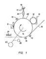
- the printing machine as shown in Fig. 1 comprises an exposure head 10 that is provided with a multiplicity of energizable pointlike radiation emitters such as 11, optical transfer means 12 for transferring the images of the emitters, and a photoreceptor in the form of a cylindrical surface of a drum 20.
- Known materials for the photoreceptor are doped selenium, polyvinyl carbazole, CdS, CdSe, SeTe, etc.
- a corona discharge station 13 electrically charges the surface of the drum 20, the sense of rotation of the drum being indicated by the arrow 14, and the drum being driven by a motor.
- the areas of the drum surface that become exposed by the emitters become discharged whereas the other, unexposed areas maintain their charge.
- the electrostatic charge pattern thus produced is developed by a developing station 15 wherein a developer composition 16 is brought into contact with the charge pattern on the drum.
- a corona transfer station 17 transfers the toner pattern from the drum surface onto a paper sheet 18 that is moved in contact with the drum.
- a corona separator station 19 is effective to separate the paper sheet from the drum.
- a fuser station 21 fuses the toner pattern on the sheet so that a permanent copy is obtained.
- a cleaner station 9 is operative to remove the toner still remaining on the drum surface therefrom before a next exposure is made.
- the photoreceptor could take some other form, e.g. the form of a belt for transferring the charge image to a suitable support, or a photosensitive sheet on which the final image is formed and fixed.
- a photosensitive sheet may e.g. comprise a support coated with a light-sensitive layer such as ZnO, silver halide, etc.
- the exposure head comprises an elongate channel section bar 22 wherein a plurality of exposure modules 23 are mounted next to each other.
- Each module comprises several arrays of emitters as will be explained further.
- the emitters of all the modules are arranged in two parallel rows 24 and 25, that run parallel with the axis of the drum 20.
- the optical transfer means 12 is an elongate element wherein a plurality of self-focussing fibers are provided, the optical axis of the transfer means, or more correctly the optical plane thereof, passing through the axis of the drum.
- each of the rows of emitters will be imaged on a respective transverse line on the photoreceptor path, namely row 24 on line 26, and row 25 on line 27, the two lines being represented by dots in the figure.
- a plurality of modules 23 are mounted next to each other in the bar 22 so that the total exposure length 1 corresponds with the desired width of the image on the photoreceptor.
- the direction of movement of the photoreceptor past the exposure head is indicated by the arrow 28.
- the modules 23 are suitably secured in the bar by means of an electrically conductive quickly curing epoxy adhesive.
- the mounting of the exposure head in the apparatus may be arranged in such a way that slight adjustments of the positioning of the head are possible, thereby to ensure a true parallel alignment of the emitter rows 24 and 25 with the photoreceptor surface.
- the module 23 comprises a metal base plate 29 onto which four different arrays 31 of emitters are mounted in abutting relationship. Each array has two rows 24 and 25 of emitters. Since in the further description, light emitting diodes will be considered for the emitters, the term LED's will hereinafter be used for these elements.
- the LED's are made on monocrystalline chips. The LED rows are staggered. The chips may as shown be cut with oblique end edges so that when chips are mounted in mutually abutting relationship as illustrated their LED's form two uninterrupted rows notwithstanding the close spacing between neighbouring LEDs of each row (see European Patent Application No. 82 201 324.9 filed the 25th October 1982).
- the modules are in their turn mounted close to each other in the bar 22 so that the slanting end edges of their end LED chips abut each other. In this way two uninterrupted rows of equally spaced LED's are obtained over the complete length of the recording head.
- the electrical connections to the base chip material of each LED, in the present example the cathodes of the LED's, are achieved via the bar 22 (Fig. 3).
- the control means for the LED's of each module are in the form of two integrated circuits 34 and 35, the circuit 34 controlling the even LED's, i.e. the LED's of row 24, and the circuit 35 controlling the odd LED's, i.e. those of row 25.
- the integrated circuits 34 and 35 are in the form of chips that likewise may be adhered to the base plate 29. Each of the chips forming the control means has a length that covers the combined LED arrays of one module.
- Each module includes a thick film structure 44 and 45 for performing the electrical connection of the circuits 34 and 35 into the apparatus.
- the mounting of the LED chips and the control chips on the base plates to form the modules, and the mounting of the modules on the bar to produce the recording head, are carried out under a microscope in view of the minute dimensions of the components.
- a microscope is also needed for making the electrical connections between the control circuits and the LED's.
- the connection between each LED and a corresponding output bonding pad of the control chip can be formed by a fine wire of aluminium that is applied by the wedge-wedge technique known in the art.
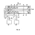
- Fig. 5 illustrates in detail the electronic circuitry of one half of a module of the recording head.
- Control chip 35 (control chips 34 being identical to chips 35) comprises a 64-steps serial-in/parallel-out shift register 36 with data bit input terminals 37 and 38, two delay registers 39 and 40, a latch register 41, sixty four individual drivers (one for each LED in the associated LED row 25), represented by one rectangular block 42, and sixty four output bonding pads 43 for the LED's in said row 25.
- the bonding pads are arranged in two staggered rows thereby to provide for more spacing between them.
- the control chips 35 comprises the following input bonding pads : The pads 37 and 38 forming the shift register input terminals referred to above, the pad 46 that receives the trigger signal for the control of the operation of the drivers 42, the pad 47 that receives a current-level control signal, the pad 48 for the clock signal that controls the serial signal shifting through the register 36, the pad 49 for the supply voltage of the drivers 42 and the LED's, the pad 50 for the supply voltage of the registers, the pads 51 and 52 for control voltages controlling the direction of signal shift through the shift register 36 and controlling the operation of the delay registers 39 and 40, the pad 53 that is for ground connection, and finally the pad 54 that is for a load control that controls the transfer of data bits from one register to the other.
- Thick film connection structure 45 (the structure 44 is identical to 45), is made on a ceramic support that may be fixed to the module 29 by adhesive bonding.
- connection structure comprises a row 55 of input bonding pads and row 56 of output bonding pads, the lateral position of which corresponds with the position of the input bonding pads of the chip 35.
- the corresponding input and output bonding pads of the structure 45 are in direct connection with each other, except for the pads 57 and 58 which are connected to each other through four series resistors 59.
- the input bonding pads 55 are connected to a printed circuit strip 70 that extends over the complete length of the recording head and that has nine conductor paths that provide the required supply voltages and control signals for the corresponding lower half of all the modules.
- a similar conductor strip 60 (fig. 6), is provided at the other side of the recording head for the connections of the control means of the upper halves of the module (see Fig. 6).
- Bonding pad 37 forms the data-bit input terminal of the chip 35, and is connected to bonding pad 61, that constitutes the output shift register terminal of the foregoing chip 35'.
- the bonding occurs via the thick film structures 45 1 and 45, and the wire connections 74, 75 and 76.
- Signals received at 37 are stepwise shifted through the shift register 36 under the control of a clock signal applied at input 48. Once the register has stepped a number of times, e.g. sixty four times in the present example, the next stepping causes the first received signal to leave the register at output pad 38 and to enter the register of the next chip 35" at input pad 62. This next chip 35" is in connection with the chip 35"' next to it, etc.
- the direction of signal shift through the register 36 depends on the selection of the input pad 51 or 52 for the reception of a D.C. setting voltage.
- the chip 35 is in fact connected into the operating circuitry of the recording head so that a D.C. voltage is applied at pad 52. Because of the internal design of the chip, the application of this D.C. voltage to pad 52 sets the chip for effecting the signal shift from left to right in response to the clock signal at 48 and at the same time renders the delay registers 39 and 40 inoperative.
- the bonding pad 54 receives the "load” signals for instructing processing of the data signals in the shift register 36.
- a load signal or in orther words a "line” signal, causes the parallel transfer of all the data bits from register 36 towards the LED drivers 42. Because the delay registers 39 and 40 of chip 35 are rendered inoperative by its setting, the data bits received by the shift register 36 of chips 35 are transferred from that shift register directly to the latch register 41 on their chips.
- the drivers 42 for the odd LED's forming row 25 are directly connected to that latch register. However although the drivers 42 receive the relevant data bit signals from the latch register 41 during each line period in response to the "load” signal, those signals cannot be released to their respective LEDs until the drivers are activated by a "trigger" signal.
- This trigger signal which activates all of the drivers 42 for the odd LEDs, is delivered at a moment which is determined by output signals from a photoreceptor speed monitor as will hereafter be described with reference to Figs. 5 to 8.
- the moment at which the drivers 42 are thus triggered is such as to preserve a predetermined uniform record line spacing on the photoreceptor.
- the chip 34 which in the aspect of Figs. 4 and 5, is located above the LED arrays 31, is identical with chip 35.
- chip 34 is inverted end for end relative to chips 35 and the data-bit input signals are supplied to both chips from the same end of the recording head (from the left in the aspect of Figs. 4 and 5) it follows that in the case of chip 34, its bonding pad 38 serves as its data-bit input terminal and its bonding pad 37 serves as its data-bit output terminal. Therefore the chip 34 is connected into the operating circuitry so that the D.C. setting voltage is applied to its pad 51, thereby setting the chip so that the signal shift through its shift register 36 also takes place from left to right in the aspect of Figs.
- Each such load signal causes transfer of data bit signals from the shift register of chip 34 to its first delay register 39 simultaneously with the transfer of previously received data-bit signals from that delay register to the second delay register 40 and with the transfer of still earlier received data-bit signals from that second delay register to the latch register of the chip. And signals transferred to that latch register can drive the connected even LEDs responsive to those signals immediately those drivers are triggered by a trigger signal transmitted responsive to photoreceptor speed fluctuation as hereinafter referred to.
- the result of the operation of the delay registers in the chip 34 is therefore that the energisation of the even LEDs forming row 24 in accordance with data-bit signals pertaining to any given information line is delayed until two line periods later than the energisation of the odd LEDs responsive to the data-bit signals pertaining to the same information line.
- This two-line delay compensates for the distance between the two rows of LEDs, of course after taking into account the mean speed of the photoreceptor.
- the precise time interval between the two energisations effecting recording of parts of any given information line is also dependent on readings of photoreceptor speed variations (if any) between the two energisations as hereafter referred to.
- the precise time interval is such as to ensure transverse alignment of the projected LED images on the photoreceptor.
- a current-level control signal determines the mean current that is produced by a driver into its corresponding LED. Reference to the "mean" current is made because owing to fabrication tolerances of drivers and LED's, the actual current through a LED may be up to e.g. 10 % larger or smaller than the desired nominal value.
- Setting of the control signal occurs by the short-circuiting of one or more of the four different series resistors 59. The resistor array enables fifteen different combinations to be made.
- the resultant control current signal is the quotient of the DC voltage, e.g. 5 V, on line 64 and the total series resistance.
- the actual current through the LED's is a number of times larger than the corresponding control current as a consequence of an amplification by a fixed factor set in the electronic circuitry of the chip 35. For instance, a control current of 500pA, may produce a mean LED current of 3 mA.
- the described technique of performing the connections of the control means of each module through an intermediary connection circuit, namely the thick film structures 45, has the advantage that if any replacement of a defective module by a good one is required at any time this can be done while leaving the fine wire connections to the other modules intact.
- the electronic block circuit of the apparatus is illustrated in Fig. 6, wherein 65 is a character generator, and 66 is a control unit wherein a clock signal is produced as well as supply voltages and trigger and load signals that are fed via several conductors represented in simplified form by the lines 67 and 68 to the printed circuit strips 60 and 70 via which they are fed to the corresponding control chips 34 and 35 of the modules.
- the clock signal controls via a line 69 a semi-conductor switch 71 that alternately applies via the lines 72 and 73 the data signals to the row 25 of odd and the row 24 of the even numbered LED's.
- 3456 LED's arranged in two staggered rows each of 1728 LED's.
- the apparatus will comprise many other circuits for the control of the different operations, such as setting and resetting circuits, synchronization circuits, stabilizing circuits, defect signalling circuits, etc.
- Such circuits are known in the art, and a description of them is not required for the understanding of the operation of the apparatus.
- the trigger control 75 is a circuit that produces on output lines 76 and 77 output impulses 78 and 79 in response to the input signals from a speed sensor 80 sensing the actual speed of the photoreceptor by measuring the speed of the drum 20 driven by a motor 87, from an optical density setter 81, and from the load impulse on line 82.
- the speed sensor may be any type of optical, inductive or other sensor that offers a high sensitivity and has a rapid response.
- a suitable sensor is an optical encoder which comprises a disc with e.g. 5000 pulses distributed along its periphery.
- impulse 79 which causes the drivers 43 on chips 35 to energise the odd LEDs forming row 25 in accordance with data bit signals from the shift register 36 commences at the end of a time interval d from the commencement of a line period.
- the impulse 79 is initiated by a "load" impulse transmitted to the trigger control circuit 75 via line 82.
- the time interval d is, in a specific example, 0.010jus.
- the remainder of the data-bit signals pertaining to that same information line should cause energisation of the even LEDs during the next but one line period at the end of an identical time interval d from the commencement of that line period.
- the pulse 79 should in those circumstances occupy the position shown in full line in Fig. 8D.
- the moment of initiation of the signal pulse 78 is automatically variable in dependence on signals deriving from the photoreceptor speed sensor 80 (Fig. 7).
- the moment of initiation of the pulse 78 is advanced or retarded.
- the 'broken lines 78 1 and 78" in Fig. 80 represent an advanced and retarded position of the pulse respectively.
- the maximum possible extents of advance and retardation are of course limited by the necessity for the pulse 78, like the pulse 79, to occur within the line period a.
- the generator 65 (Fig. 6) produces data-bit signals for the recording of the first image line to be recorded on the photoreceptor.
- Switch 71 is controlled by the clock frequency, e.g. a frequency of the order of magnitude of 3 Mhz, such that the signal for the first image point of the first image line is put on line 72, the signal for the second image point is put on line 73, the next signal on line 72, the still next on line 73, etc., until finally 1728 distinct (odd) image points have been read-in in the shift registers 36 of the control chips 35, and 1728 image (even) image points have been read-in in the shift registers 36 of the control chips 34.
- the total number of 3456 image points is determined by the use of the recording head of 27 modules with 128 LED"s each.
- Appropriate low impulse signals are transmitted by control unit 66 via lines 67 and 68 to the input pads 54 of the control chips 34 and 35 so that the chips 35 are caused to pass their data signals in parallel directly from their shift registers 36 to their latch registers 41, so that these signals become applied to the corresponding odd LED's in response to the pulse 79; and the control chips 34 are caused to pass their data signals in parallel from their shift registers 36 to their first delay registers 39.
- the latch registers 41 are reset by an appropriate signal, and data signals representing of chips 35 the second image line to be recorded are produced by the generator 65.
- the odd information signals are directly recorded as for the previous lines, whereas the even signals stored in each of the registers of control chips 34 are advanced one step : the signals stored in their shift registers are transferred to their delay register 39; the signals previously stored in those registers are transferred to their delay registers 40, and the signals previously stored in those registers are transferred to their latch registers 41 and become recorded immediately the drivers of the even LEDs are triggered by the next pulse 78.
- the recording of the even image points belonging to a given information line is therefore delayed by two line periods (plus or minus the automatic adjustment for photoreceptor speed fluctuation) relative to the recording of the odd image points belonging to that line. This delay compensates for the distance between the two rows of LED's, which is twice the distance between successive raster lines on the photoreceptor.
- clock frequency 3 Mhz resistors 59 : 4, 2, 1 and 0,5 Kohms arranged for trimming optical transfer means 12 : a Selfoc, type SLA 20, manufactured by Nippon sheet glass Co., Ltd. motor driving the photoreceptor : asymchronous A.C. motor, 75 watts. recording speed : 10 cm.s l .
- the present invention is not limited to the above described embodiment.
- control chips 34 and 35 need not necessarily be identical.
- control chips 35 may be replaced by chips which differ from the chips 34 in that they are without delay registers. However, as previously stated, this would not necessarily mean a cost saving for the apparatus.
- the recording head of the apparatus may comprise more than two staggered rows of sources of radiation, each row other than the first row being associated with its own particular delay, and trigger control.
- the modules may comprise one large array of LED's, instead of four smaller arrays as described.
- the modules may also comprise parallel rows of chips each having a single rows of LED's, the chips of the different rows being in staggered relation as disclosed in the EU-application 82 201 324.9 relating to a recording apparatus for linewise recording information upon a moving photoreceptor.
Landscapes
- Engineering & Computer Science (AREA)
- Multimedia (AREA)
- Signal Processing (AREA)
- Printers Or Recording Devices Using Electromagnetic And Radiation Means (AREA)
- Exposure Or Original Feeding In Electrophotography (AREA)
- Facsimile Heads (AREA)
- Fax Reproducing Arrangements (AREA)
- Dot-Matrix Printers And Others (AREA)
- Record Information Processing For Printing (AREA)
- Facsimile Transmission Control (AREA)
- Optical Recording Or Reproduction (AREA)
Priority Applications (5)
| Application Number | Priority Date | Filing Date | Title |
|---|---|---|---|
| EP83201561A EP0142579B1 (de) | 1983-11-01 | 1983-11-01 | Aufzeichnungsgerät |
| DE8383201561T DE3376728D1 (en) | 1983-11-01 | 1983-11-01 | Recording apparatus |
| CA000466298A CA1230637A (en) | 1983-11-01 | 1984-10-25 | Recording apparatus |
| US06/665,521 US4575739A (en) | 1983-11-01 | 1984-10-26 | Recording apparatus |
| JP59230034A JPH0747319B2 (ja) | 1983-11-01 | 1984-10-31 | 記録用装置 |
Applications Claiming Priority (1)
| Application Number | Priority Date | Filing Date | Title |
|---|---|---|---|
| EP83201561A EP0142579B1 (de) | 1983-11-01 | 1983-11-01 | Aufzeichnungsgerät |
Publications (2)
| Publication Number | Publication Date |
|---|---|
| EP0142579A1 true EP0142579A1 (de) | 1985-05-29 |
| EP0142579B1 EP0142579B1 (de) | 1988-05-18 |
Family
ID=8191007
Family Applications (1)
| Application Number | Title | Priority Date | Filing Date |
|---|---|---|---|
| EP83201561A Expired EP0142579B1 (de) | 1983-11-01 | 1983-11-01 | Aufzeichnungsgerät |
Country Status (5)
| Country | Link |
|---|---|
| US (1) | US4575739A (de) |
| EP (1) | EP0142579B1 (de) |
| JP (1) | JPH0747319B2 (de) |
| CA (1) | CA1230637A (de) |
| DE (1) | DE3376728D1 (de) |
Cited By (4)
| Publication number | Priority date | Publication date | Assignee | Title |
|---|---|---|---|---|
| EP0214674A1 (de) * | 1985-09-05 | 1987-03-18 | Agfa-Gevaert N.V. | Verfahren zum Justieren der Lichtausstrahlung einer Leuchtdiode bei einem vorgegebenen Treibstrom |
| BE1004579A5 (fr) * | 1990-07-02 | 1992-12-15 | Creo Products Inc | Modulateur de lumiere pour sources lumineuses a grande surface. |
| DE102012024359A1 (de) * | 2012-12-13 | 2014-06-18 | Tichawa IP GmbH | Sensoranordnung zur zeilenweisen optischen Abtastung |
| EP3528295A1 (de) * | 2012-02-10 | 2019-08-21 | Facebook Technologies, LLC | Anzeigevorrichtung mit leuchtdiodenchip und verfahren zu deren herstellung |
Families Citing this family (23)
| Publication number | Priority date | Publication date | Assignee | Title |
|---|---|---|---|---|
| WO1986002045A1 (fr) * | 1984-09-27 | 1986-04-10 | Sanyo Electric Co., Ltd. | Tete imprimante optique pour appareil a impression optique |
| NL8403926A (nl) * | 1984-12-24 | 1986-07-16 | Oce Nederland Bv | Werkwijze voor het belichten van een lichtgevoelige laag en belichtingsinrichting. |
| JPS62104363A (ja) * | 1985-10-31 | 1987-05-14 | Yokogawa Medical Syst Ltd | 多駒写真撮影装置 |
| JPS62137964A (ja) * | 1985-12-12 | 1987-06-20 | Fuji Xerox Co Ltd | 光書き込みヘツド |
| JPS62140859A (ja) * | 1985-12-16 | 1987-06-24 | Brother Ind Ltd | 感光体記録装置 |
| JPH0513577Y2 (de) * | 1986-01-28 | 1993-04-09 | ||
| JPH0439011Y2 (de) * | 1986-01-30 | 1992-09-11 | ||
| US4941004A (en) * | 1987-04-01 | 1990-07-10 | Eastman Kodak Company | Printer apparatus |
| US4829321A (en) * | 1987-04-23 | 1989-05-09 | Hitachi Cable, Ltd. | Optical printer head with a light emitting diode array |
| US5225848A (en) * | 1989-12-27 | 1993-07-06 | Am International, Inc. | Imaging diode array and system |
| US5420616A (en) * | 1990-01-23 | 1995-05-30 | Fuji Xerox Co., Ltd | Electrostatic recording method and apparatus with recording head timing control |
| US5081476A (en) * | 1990-04-04 | 1992-01-14 | Xerox Corporation | Ionographic printhead gating control for controlling charge density image defects due to surface velocity variations |
| JPH0416866A (ja) * | 1990-05-10 | 1992-01-21 | Canon Inc | 画像形成装置 |
| EP0461437B1 (de) * | 1990-05-22 | 1998-07-29 | Canon Kabushiki Kaisha | Datenaufzeichnungsgerät |
| JP3255409B2 (ja) * | 1990-11-29 | 2002-02-12 | キヤノン株式会社 | 画像形成装置 |
| US5231428A (en) * | 1990-12-11 | 1993-07-27 | Xerox Corporation | Imaging device which compensates for fluctuations in the speed of an image receiving surface |
| US5274394A (en) * | 1991-05-22 | 1993-12-28 | Xerox Corporation | Electronic adjustment of slow scan image registration in an image recording apparatus |
| US5250960A (en) * | 1991-12-31 | 1993-10-05 | Xerox Corporation | System and method employing multiple pulses per pixel to reproduce an image |
| JP3381582B2 (ja) * | 1997-06-27 | 2003-03-04 | カシオ電子工業株式会社 | 光書き込みヘッド駆動装置、及びその装置を使用する光書き込みヘッド駆動方法 |
| WO2002020272A1 (fr) * | 2000-09-05 | 2002-03-14 | Nippon Sheet Glass Co.,Ltd. | Reseau de dispositifs luminescents auto-balayes, son procede et son circuit d'entrainement |
| JP2004082583A (ja) * | 2002-08-28 | 2004-03-18 | Oki Data Corp | Ledヘッドおよび画像形成装置 |
| AU2004297504B9 (en) * | 2003-11-21 | 2010-06-03 | W.R. Grace & Co.-Conn. | Sulfate dispersion chromate reducer |
| US7510256B2 (en) * | 2005-03-30 | 2009-03-31 | Xerox Corporation | Reflex printing with process direction stitch error correction |
Citations (5)
| Publication number | Priority date | Publication date | Assignee | Title |
|---|---|---|---|---|
| FR2463680A1 (fr) * | 1979-08-21 | 1981-02-27 | Oki Electric Ind Co Ltd | Tete d'impression optique pour des imprimantes optiques |
| EP0050481A2 (de) * | 1980-10-16 | 1982-04-28 | Fuji Xerox Co., Ltd. | Gerät zur Aufzeichnung vielfarbiger Bilder |
| EP0051978A2 (de) * | 1980-11-11 | 1982-05-19 | Fuji Photo Film Co., Ltd. | Verfahren zum Einstellen der Dichte bei einer Bildreproduktion |
| EP0051886A1 (de) * | 1980-11-10 | 1982-05-19 | Agfa-Gevaert N.V. | Aufzeichnungsvorrichtung |
| GB2099221A (en) * | 1981-05-26 | 1982-12-01 | Purdy Haydn Victor | Light emitting diode array devices and image transfer systems |
Family Cites Families (6)
| Publication number | Priority date | Publication date | Assignee | Title |
|---|---|---|---|---|
| JPS52153319A (en) * | 1976-06-15 | 1977-12-20 | Matsushita Graphic Communic | Signal processing system for facsimile transmission systems |
| DE2631849A1 (de) * | 1976-07-15 | 1978-01-19 | Agfa Gevaert Ag | Aufzeichnungsvorrichtung |
| JPS56132357A (en) * | 1980-03-21 | 1981-10-16 | Konishiroku Photo Ind Co Ltd | Information recorder |
| JPS5726874A (en) * | 1980-07-24 | 1982-02-13 | Ricoh Co Ltd | Electrophotographic type printer device |
| JPS58134766A (ja) * | 1982-02-04 | 1983-08-11 | Seiko Instr & Electronics Ltd | 感熱記録装置 |
| US4445796A (en) * | 1982-06-16 | 1984-05-01 | International Business Machines Corporation | Print electrode control circuit |
-
1983
- 1983-11-01 DE DE8383201561T patent/DE3376728D1/de not_active Expired
- 1983-11-01 EP EP83201561A patent/EP0142579B1/de not_active Expired
-
1984
- 1984-10-25 CA CA000466298A patent/CA1230637A/en not_active Expired
- 1984-10-26 US US06/665,521 patent/US4575739A/en not_active Expired - Lifetime
- 1984-10-31 JP JP59230034A patent/JPH0747319B2/ja not_active Expired - Lifetime
Patent Citations (5)
| Publication number | Priority date | Publication date | Assignee | Title |
|---|---|---|---|---|
| FR2463680A1 (fr) * | 1979-08-21 | 1981-02-27 | Oki Electric Ind Co Ltd | Tete d'impression optique pour des imprimantes optiques |
| EP0050481A2 (de) * | 1980-10-16 | 1982-04-28 | Fuji Xerox Co., Ltd. | Gerät zur Aufzeichnung vielfarbiger Bilder |
| EP0051886A1 (de) * | 1980-11-10 | 1982-05-19 | Agfa-Gevaert N.V. | Aufzeichnungsvorrichtung |
| EP0051978A2 (de) * | 1980-11-11 | 1982-05-19 | Fuji Photo Film Co., Ltd. | Verfahren zum Einstellen der Dichte bei einer Bildreproduktion |
| GB2099221A (en) * | 1981-05-26 | 1982-12-01 | Purdy Haydn Victor | Light emitting diode array devices and image transfer systems |
Cited By (5)
| Publication number | Priority date | Publication date | Assignee | Title |
|---|---|---|---|---|
| EP0214674A1 (de) * | 1985-09-05 | 1987-03-18 | Agfa-Gevaert N.V. | Verfahren zum Justieren der Lichtausstrahlung einer Leuchtdiode bei einem vorgegebenen Treibstrom |
| BE1004579A5 (fr) * | 1990-07-02 | 1992-12-15 | Creo Products Inc | Modulateur de lumiere pour sources lumineuses a grande surface. |
| EP3528295A1 (de) * | 2012-02-10 | 2019-08-21 | Facebook Technologies, LLC | Anzeigevorrichtung mit leuchtdiodenchip und verfahren zu deren herstellung |
| DE102012024359A1 (de) * | 2012-12-13 | 2014-06-18 | Tichawa IP GmbH | Sensoranordnung zur zeilenweisen optischen Abtastung |
| DE102012024359B4 (de) * | 2012-12-13 | 2014-10-30 | Tichawa IP GmbH | Sensoranordnung zur zeilenweisen optischen Abtastung |
Also Published As
| Publication number | Publication date |
|---|---|
| JPS60132460A (ja) | 1985-07-15 |
| EP0142579B1 (de) | 1988-05-18 |
| US4575739A (en) | 1986-03-11 |
| CA1230637A (en) | 1987-12-22 |
| JPH0747319B2 (ja) | 1995-05-24 |
| DE3376728D1 (en) | 1988-06-23 |
Similar Documents
| Publication | Publication Date | Title |
|---|---|---|
| US4575739A (en) | Recording apparatus | |
| US4571602A (en) | Recording apparatus | |
| EP0115088B1 (de) | Aufzeichnungsgerät | |
| EP0086907B1 (de) | Aufzeichnungsapparat | |
| US4706130A (en) | Image recording apparatus utilizing light emitting diodes with pixel shape correction | |
| EP0307994B1 (de) | Belichtungseinrichtung mit Alterungs-Korrekturanordnung für LED-Drucker | |
| EP0585022B1 (de) | Verfahren und Vorrichtung zur seitlichen Registrierung von aufeinanderfolgenden Bildern mit einem Vielfach-LED-Zeilendrucksystem in einem einzelnen Durchgang | |
| EP0299012B1 (de) | Schaltung zur erzeugung von zentralimpulsbreitemodulierten signalen und damit ausgerüsteter einschlagsloser drucker | |
| EP0247699B1 (de) | Bildaufzeichnungsträger für einen elektrostatischen Drucker und Drucker, in dem ein Träger dieser Art benutzt wird | |
| EP0088555B1 (de) | Punktmatrixdruckmethode und Drucker hierfür | |
| US5300961A (en) | Method and apparatus for aligning multiple print bars in a single pass system | |
| US5040074A (en) | Full-width simultaneous read/write copier | |
| US5160837A (en) | Light emitter array diagnostic apparatus | |
| US5272493A (en) | Method and apparatus for registration of sequential images in a single pass, multi-LED printbar printer | |
| US5294942A (en) | Non-impact printer apparatus and method for recording on a moving medium | |
| US5121145A (en) | Line printhead device for nonimpact printer | |
| EP0381282B1 (de) | Verfahren und Gerät für bildweise Belichtung einer lichtempfindlichen Vorlage unter Verwendung einer Anzahl von Lichtventilen | |
| EP0034066A2 (de) | Druckgerät mit Formulareinspiegelung | |
| EP0349628B1 (de) | Elektro-optisches aufzeichnungsgerät mit aufzeichnung gemäss mehreren auflösungen | |
| EP0437023A2 (de) | Belichtungssteuerung von Energiequellen | |
| JPS62240919A (ja) | 画像記録装置 | |
| JP2001080118A (ja) | 光書き込み装置 | |
| JPH1128834A (ja) | プリントヘッドおよび画像形成装置 | |
| JPH0517038A (ja) | 画像形成装置 |
Legal Events
| Date | Code | Title | Description |
|---|---|---|---|
| PUAI | Public reference made under article 153(3) epc to a published international application that has entered the european phase |
Free format text: ORIGINAL CODE: 0009012 |
|
| AK | Designated contracting states |
Designated state(s): AT BE CH DE FR GB IT LI LU NL SE |
|
| 17P | Request for examination filed |
Effective date: 19851021 |
|
| 17Q | First examination report despatched |
Effective date: 19870728 |
|
| GRAA | (expected) grant |
Free format text: ORIGINAL CODE: 0009210 |
|
| AK | Designated contracting states |
Kind code of ref document: B1 Designated state(s): BE DE FR GB IT NL |
|
| REF | Corresponds to: |
Ref document number: 3376728 Country of ref document: DE Date of ref document: 19880623 |
|
| ITF | It: translation for a ep patent filed | ||
| ET | Fr: translation filed | ||
| PLBI | Opposition filed |
Free format text: ORIGINAL CODE: 0009260 |
|
| 26 | Opposition filed |
Opponent name: OCE-NEDERLAND B.V., VENLO Effective date: 19890214 |
|
| NLR1 | Nl: opposition has been filed with the epo |
Opponent name: OCE-NEDERLAND B.V. |
|
| PLBN | Opposition rejected |
Free format text: ORIGINAL CODE: 0009273 |
|
| STAA | Information on the status of an ep patent application or granted ep patent |
Free format text: STATUS: OPPOSITION REJECTED |
|
| 27O | Opposition rejected |
Effective date: 19910510 |
|
| NLR2 | Nl: decision of opposition | ||
| ITTA | It: last paid annual fee | ||
| PGFP | Annual fee paid to national office [announced via postgrant information from national office to epo] |
Ref country code: GB Payment date: 19951020 Year of fee payment: 13 Ref country code: FR Payment date: 19951020 Year of fee payment: 13 |
|
| PGFP | Annual fee paid to national office [announced via postgrant information from national office to epo] |
Ref country code: BE Payment date: 19951023 Year of fee payment: 13 |
|
| PGFP | Annual fee paid to national office [announced via postgrant information from national office to epo] |
Ref country code: NL Payment date: 19951213 Year of fee payment: 13 |
|
| PG25 | Lapsed in a contracting state [announced via postgrant information from national office to epo] |
Ref country code: GB Effective date: 19961101 |
|
| PG25 | Lapsed in a contracting state [announced via postgrant information from national office to epo] |
Ref country code: BE Effective date: 19961130 |
|
| BERE | Be: lapsed |
Owner name: AGFA-GEVAERT N.V. Effective date: 19961130 |
|
| PG25 | Lapsed in a contracting state [announced via postgrant information from national office to epo] |
Ref country code: NL Effective date: 19970601 |
|
| GBPC | Gb: european patent ceased through non-payment of renewal fee |
Effective date: 19961101 |
|
| PG25 | Lapsed in a contracting state [announced via postgrant information from national office to epo] |
Ref country code: FR Effective date: 19970731 |
|
| NLV4 | Nl: lapsed or anulled due to non-payment of the annual fee |
Effective date: 19970601 |
|
| REG | Reference to a national code |
Ref country code: FR Ref legal event code: ST |
|
| PGFP | Annual fee paid to national office [announced via postgrant information from national office to epo] |
Ref country code: DE Payment date: 20021004 Year of fee payment: 20 |
|
| APAH | Appeal reference modified |
Free format text: ORIGINAL CODE: EPIDOSCREFNO |