EP0142723B1 - Frequenzwandler für Multiplexsystem unter Verwendung des Stopfverfahrens - Google Patents
Frequenzwandler für Multiplexsystem unter Verwendung des Stopfverfahrens Download PDFInfo
- Publication number
- EP0142723B1 EP0142723B1 EP84112651A EP84112651A EP0142723B1 EP 0142723 B1 EP0142723 B1 EP 0142723B1 EP 84112651 A EP84112651 A EP 84112651A EP 84112651 A EP84112651 A EP 84112651A EP 0142723 B1 EP0142723 B1 EP 0142723B1
- Authority
- EP
- European Patent Office
- Prior art keywords
- pulse
- stuffing
- clock
- signal
- frame
- Prior art date
- Legal status (The legal status is an assumption and is not a legal conclusion. Google has not performed a legal analysis and makes no representation as to the accuracy of the status listed.)
- Expired
Links
Images


Classifications
-
- H—ELECTRICITY
- H04—ELECTRIC COMMUNICATION TECHNIQUE
- H04J—MULTIPLEX COMMUNICATION
- H04J3/00—Time-division multiplex systems
- H04J3/02—Details
- H04J3/06—Synchronising arrangements
- H04J3/07—Synchronising arrangements using pulse stuffing for systems with different or fluctuating information rates or bit rates
Definitions
- the present invention relates to a frequency converter which converts frequency of stuffing pulse applied.
- an input signal is once stored in a memory and such signal is read from said memory with a clock which is higherthan the write clock.
- the write clock and read clock are respectively different in repetition frequency and therefore the phase difference between write clock and read clock becomes small gradually and the same input signal is sometimes read twice.
- the stuffing designation pulse has a 3-bit structure to allow for transmission error, and the presence of a stuffing pulse was determined on the basis of majority decision at the receiving side.
- the above object can be attained by providing:
- the presence or absence of said stuffing pulse is indicated by logic "1" and "0" forming said frame synchronization signal.
- the presence or absence of a stuffing pulse can be indicated by the stuffing designation pulse of 1 bit and therefore the stuffing designation pulse can be transmitted ever where the difference between repetition frequencies of write and read clocks is small.
- the stuffing designation pulse is formed by one bit but it does not influence transmission error.
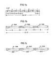
- Figure 1 shows an example of the frame format where a PCM multiplex signal with clock frequency of 704 kb/s is synchronously converted to a PCM (pulse code modulation) multiplex signal with clock frequency of 710.618 kb/s.
- the main frame is composed of eight subframes and each subframe is composed, as shown in Figure 1(b), of three G frames, namely, G1, G2 and G3 frames.
- the GI frame consists of a subframe synchronization pulse F and data pulses D of 84 bits
- the G2 frame consists of an SF pulse which is used in common as the main frame synchronization pulse of 1 bit and a stuffing designation pulse, and of D pulses of 84 bits
- G3 frame consists of the stuffing pulse V of 1 bit and D pulses of 84 bits.
- One subframe is composed of 255 bits.
- the code train 10101011 is assigned bit by bit to the SF pulse of the G2 frame and such code train is repeated for every eight subframes. Thus, it is repeated with the period of the main frame.
- the code "0" indicates that the stuffing pulse exists (is present), while the code "1" indicates that the stuffing pulse does not exist (is absent).
- the subframe of Figure 1 (c) is also composed of three G frames.
- the subframe synchronization pulse F of the first G1 frame is sent through repetition of the code train 10101011
- the main frame synchronization pulse F of the second G2 frame is sent through repetition of the inverted code train 01010100
- the frame synchronization pulse of the third G3 frame is also located at the position of the stuffing pulse V.
- presence or absence of the stuffing pulse can be determined by the code of frame synchronization pulse F.
- FIG. 2 shows buffer memories 1, 11, phase locked loop (PLL) circuits 2, 12, a stuffing control circuit 3, frequency dividers 4, 14, a frame signal generator 5, a pulse inserter 6, a destuffing control circuit 13, a synchronization circuit 15, and a clock extraction circuit 16.
- PLL phase locked loop
- the data (a) of a low order group signal are written into the buffer memory 1 in synchronization with the clock b at the bit rate of 704kb/s sent from the PLL 2.
- This clock b is generated as indicated below from the high order group signal clock e.
- the clock (e) is divided by the divider 4 to the basic frequency required for forming the frame and is then subjected to the stuffing control (extraction of clock) in the stuffing control circuit 3 so that a constant stuffing rate can be obtained (3/8 in the example of Figure 1).
- the output pulse train (c) of stuffing control circuit 3 receives the extracted pulse of 704 kb/s at such a timing of the leading bit position of the G3 frame when the main frame synchronization pulse SF is "0" and the read operation of data from the buffer memory 1 is inhibited. Moreover, the phase of the output pulse train (c) is synchronized by the PLL circuit 2 and such pulse is produced as the low order group signal clock (b). Simultaneously, the output of frequency divider 4 is used to drive a frame signal generator 5 in order to generate the required frame signal and to form a frame as shown in Figure 1 at the pulse inserter 6.
- the phase comparator of PLL 2 compares the phase of an output of the voltage controlled oscillator and the phase of read clock (c) and therefore it is enough for the buffer memory 1 to have the capacitance for absorbing only fluctuations of phase due to the frame bit, stuffing bit and stuffing designation pulse insertion.
- the data signal written in the buffer memory 1 is read by the clock (c) and is then sent to the pulse inserter 6 as the data (g).
- the pulse inserter 6 the frame signal is inserted into the data as described above and the frame as shown in Figure 1 is formed and is supplied to the transmission line as the synchronized data output (f).
- the timing where the main frame synchronization pulse SF becomes "0" matches the timing where read operation of buffer memory 1 is inhibited.
- the data (g) to be input to the pulse inserter 6 is logic "0" and it becomes the stuffing pulse.
- the synchronized data output (f) sent to the transmission line is sent to the clock extraction circuit 16 in the receiving side shown in Figure 2 (b) and the synchronized clock (r) is extracted.
- the subframe synchronization pulse F and the main frame synchronization signal SF are removed from the synchronized data (q) in the synchronizer 15 and only the signal (p) of data is written into the buffer memory 11.
- the synchronized clock input (r) is divided by the divider 14 and sub and main frame synchronization signal extraction timing is supplied to the synchronizer 15, while the timing signal for writing data to the buffer memory 11 is supplied simultaneously to the destuffing controller 13.
- the data which indicates presence or absence of stuffing pulses in the sending side is contained in the code train of the main frame synchronization signal SF and it is also used as the stuffing designation pulse.
- the data corresponding to the stuffing designation pulse can be obtained from the code train of multiframe synchronization signal SF.
- the data for determining presence or absence of stuffing pulse V can be obtained.
- the multiframe synchronization signal SF indicates that the stuffing pulse does not exist when it is "1". Therefore, the pulse in this case is judged as valid. On the other hand, it indicates that the stuffing pulse exists when it is "0". In this case, the pulse is judged as invalid.
- the destuffing controller 13 supplies the clock (n) to the buffer memory so that the valid pulse is written to the buffer memory 11 but writing of invalid pulse is inhibited.
- Such clock pulses are extracted and the phases of them are averaged by the PLL circuit 12 and the original low order group signal clock (m) can be recovered as the output thereof.
- the data of buffer memory 11 is read by such recovered clock (m) and thereby the low order group data output (I) can be obtained.
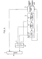
- FIG. 4 The same Figures show a clock (e) generator 10; NAND gates 31, 51, 52, 53, 61; frequency dividers 41, 42, 43; an AND gate 32 with inhibit input; and an AND gate 62.
- the signal waveforms of respective portions in Figure 3 are indicated by the same symbols in Figure 4.
- F is the code train of the subframe synchronization signal
- SF is the code train of the multiframe synchronization signal
- FF is the frame format.
- the clock (e) generated by the generator 10 is supplied to a divider 4 and is then divided to 1/85 by the divider 41 and is then output as the clock CL1, because one G frame is composed of 85 bits.
- the clock CL1 indicates the frame signal position of each G frame.
- the clock CL1 is further divided into 1/3 by the divider 42 and is then output as the clocks CL2, CL3, CL4 having different phases.
- the falling part of clock CL2 indicates the heading part of G1 frame, while that of CL3 the heading part of G2 frame and that of CL4 the heading part of G3 frame respectively.
- the clock CL2 is supplied to the divider 43 and the clock CL5 divided to 1/2 and the clock CL6 divided to 3/8 are produced therefrom.
- the clocks CL1, CL2, CL5 are supplied to the NAND gate 51 and the subframe synchronization signal F is produced therefrom.
- the clocks CL1, CL3, CL6 are supplied to the NAND gate 52 and the main frame synchronization signal (namely, the stuffing designation pulse) SF is output.
- the clocks CL1, CL4, CL6 are input to the NAND gate 31 and the stuffing control pulse SFP which conducts extraction of clock (e) three times for each multiframe can be produced.
- NAND gate 31 An output of NAND gate 31 is supplied to the inverting input terminal of AND gate 32.
- the clock (e) is supplied to the other input of the AND gate 32 and the clock (c) which is extracted by the stuffing control pulse SFP as described above is output.
- the subframe synchronization signal F and main frame synchronization signal are supplied to the NAND gate 53 and also to the NAND gate 61 and AND gate 62 of the pulse inserter 6 as the synchronization signal (d).
- An input signal read from the buffer memory 1 is supplied to the other input of NAND gate 61 but it is inhibited to produce the signal in accordance with the pattern of synchronization signal by the subframe synchronization signal F and the main frame synchronization signal SF.
- an output of the NAND gate 61 becomes logic "1"
- the subframe synchronization signal F and the main frame synchronization signal SF are supplied from the AND gate 62.
- the subframe synchronization signal F and main frame synchronization signal SF are removed from the synchronized data but an output of divider 14 is fed back to the synchronization circuit 15 in order to lock the phases of the output of divider 14 and the synchronized data (q).
- the frequency dividing circuits 141, 142, 143 forming the divider 14 respectively have the same functions as the frequency dividing circuits 41 42, 43.
- an output of the dividing circuit 141, an output of the dividing circuit 142 corresponding to the clock CL4 of the dividing circuit 42 and an output of the dividing circuit 143 corresponding to the clock CL6 of dividing circuit 43 are supplied to the NAND gate 131 which forms the destuffing control circuit 13, in order to know the destuffing timing.
- the pulse indicated as SFP in Figure 4 is supplied to the buffer memory 11 from the NAND gate 131.
- the buffer memory 11 inhibits writing of synchronized data when the pulse SFP is generated.
- the multiframe synchronization signal is used also as the stuffing designation pulse. Therefore, the stuffing designation pulse can be transmitted even when the conversion ratio is small.
Landscapes
- Engineering & Computer Science (AREA)
- Computer Networks & Wireless Communication (AREA)
- Signal Processing (AREA)
- Time-Division Multiplex Systems (AREA)
- Synchronisation In Digital Transmission Systems (AREA)
Claims (1)
- Frequenzwandler, der Frequenz durch Einfügen von Stopfimpulsen in Multiplexsignale umwandelt, mit Mitteln (1,3) zum Einfügen der Stopfimpulse; und Mitteln (6) zum Andeuten des Vorhandenseins oder Nichtvorhandenseins des Stopfimpulses und zum Einfügen des Rahmensynchronisationssignals für Rahmensynchronisation, wodurch das Vorhandensein oder Nichtvorhandensein des Stopfimpulses durch einen stopfkennzeichnenden Impuls angedeutet wird, dadurch gekennzeichnet, daß der stopfkennzeichnende Impuls aus einem Bit besteht, entweder Logik "1" oder "0" ist, und das Rahmensynchronisationssignal bildet.
Applications Claiming Priority (2)
| Application Number | Priority Date | Filing Date | Title |
|---|---|---|---|
| JP195593/83 | 1983-10-19 | ||
| JP58195593A JPH069346B2 (ja) | 1983-10-19 | 1983-10-19 | 同期伝送のための周波数変換方法 |
Publications (3)
| Publication Number | Publication Date |
|---|---|
| EP0142723A2 EP0142723A2 (de) | 1985-05-29 |
| EP0142723A3 EP0142723A3 (en) | 1988-01-27 |
| EP0142723B1 true EP0142723B1 (de) | 1990-06-13 |
Family
ID=16343725
Family Applications (1)
| Application Number | Title | Priority Date | Filing Date |
|---|---|---|---|
| EP84112651A Expired EP0142723B1 (de) | 1983-10-19 | 1984-10-19 | Frequenzwandler für Multiplexsystem unter Verwendung des Stopfverfahrens |
Country Status (5)
| Country | Link |
|---|---|
| US (1) | US4885746A (de) |
| EP (1) | EP0142723B1 (de) |
| JP (1) | JPH069346B2 (de) |
| CA (1) | CA1262937A (de) |
| DE (1) | DE3482540D1 (de) |
Families Citing this family (10)
| Publication number | Priority date | Publication date | Assignee | Title |
|---|---|---|---|---|
| JPH0697759B2 (ja) * | 1985-10-16 | 1994-11-30 | 株式会社日立製作所 | デジタル信号の同期化方式 |
| CA1332627C (en) * | 1987-03-17 | 1994-10-18 | Antonio Cantoni | Jitter control in digital communications links |
| JPH0693667B2 (ja) * | 1988-08-03 | 1994-11-16 | 富士通株式会社 | 同期多重方式 |
| DE3922897A1 (de) * | 1989-07-12 | 1991-01-17 | Philips Patentverwaltung | Stopfentscheidungsschaltung fuer eine anordnung zur bitratenanpassung |
| FR2675924B1 (fr) * | 1991-04-25 | 1993-12-24 | Innovatron Sa | Systeme d'echange de donnees entre un objet electronique accouple a un dispositif de transfert a debits de donnees distincts, objet inserable et dispositif de transfert correspondants. |
| JP3078183B2 (ja) * | 1994-09-26 | 2000-08-21 | 沖電気工業株式会社 | データ受信装置 |
| US5757869A (en) * | 1995-07-28 | 1998-05-26 | Adtran, Inc. | Apparatus and method for detecting frame synchronization pattern/word in bit-stuffed digital data frame |
| EP2276023A3 (de) * | 2005-11-30 | 2011-10-05 | Telefonaktiebolaget LM Ericsson (publ) | Effiziente sprach-strom-umsetzung |
| US8880928B2 (en) * | 2008-04-11 | 2014-11-04 | Thinklogical, Llc | Multirate transmission system and method for parallel input data |
| US9026434B2 (en) * | 2011-04-11 | 2015-05-05 | Samsung Electronic Co., Ltd. | Frame erasure concealment for a multi rate speech and audio codec |
Family Cites Families (8)
| Publication number | Priority date | Publication date | Assignee | Title |
|---|---|---|---|---|
| BE638811A (de) * | 1962-10-18 | |||
| CH504818A (de) * | 1968-12-11 | 1971-03-15 | Standard Telephon & Radio Ag | Verfahren zur Datenübertragung über einen Kanal einer PCM-Nachrichtenanlage |
| US3946161A (en) * | 1970-10-26 | 1976-03-23 | Communications Satellite Corporation | Distributed bit stuff decision transmission |
| US3825899A (en) * | 1971-08-11 | 1974-07-23 | Communications Satellite Corp | Expansion/compression and elastic buffer combination |
| FR2269246B1 (de) * | 1974-04-25 | 1976-12-17 | Cit Alcatel | |
| US4010325A (en) * | 1975-10-30 | 1977-03-01 | Gte Automatic Electric Laboratories Incorporated | Framing circuit for digital signals using evenly spaced alternating framing bits |
| US4596026A (en) * | 1983-05-09 | 1986-06-17 | Raytheon Company | Asynchronous data clock generator |
| CA1232693A (en) * | 1985-09-05 | 1988-02-09 | Alan F. Graves | Network multiplex structure |
-
1983
- 1983-10-19 JP JP58195593A patent/JPH069346B2/ja not_active Expired - Lifetime
-
1984
- 1984-10-18 CA CA000465727A patent/CA1262937A/en not_active Expired
- 1984-10-19 DE DE8484112651T patent/DE3482540D1/de not_active Expired - Lifetime
- 1984-10-19 EP EP84112651A patent/EP0142723B1/de not_active Expired
-
1985
- 1985-04-29 US US06/728,191 patent/US4885746A/en not_active Expired - Lifetime
Also Published As
| Publication number | Publication date |
|---|---|
| EP0142723A2 (de) | 1985-05-29 |
| JPS6087539A (ja) | 1985-05-17 |
| JPH069346B2 (ja) | 1994-02-02 |
| DE3482540D1 (de) | 1990-07-19 |
| EP0142723A3 (en) | 1988-01-27 |
| CA1262937A (en) | 1989-11-14 |
| US4885746A (en) | 1989-12-05 |
Similar Documents
| Publication | Publication Date | Title |
|---|---|---|
| US5623512A (en) | Rate converting device capable of determining a transmission rate as desired | |
| KR910001743B1 (ko) | 데이타 멀티 플렉스 전송 장치 | |
| US4543652A (en) | Time-division switching unit | |
| EP0142723B1 (de) | Frequenzwandler für Multiplexsystem unter Verwendung des Stopfverfahrens | |
| EP0178622A2 (de) | Taktwiedergewinnungsschaltung für Manchester-kodierte Daten | |
| ATE55524T1 (de) | Synchronisation nachziehbarer taktoszillatoren bei der uebertragung digitaler signale. | |
| US4669080A (en) | Synchronizing circuit in a plesiochronous digital signal multiplexer | |
| US5708685A (en) | Frame synchronous signal detector | |
| CA2520906C (en) | Method and apparatus for frame alignment | |
| US4679188A (en) | Digital transmission system | |
| US4773084A (en) | Synchronizing pattern | |
| JPH0748725B2 (ja) | フレーム同期回路 | |
| US5444658A (en) | Elastic store memory circuit | |
| JP2697371B2 (ja) | スタッフ多重通信受信回路 | |
| US5548624A (en) | Destuff circuit for asynchronous digital signals | |
| CA2063000C (en) | Method and circuit for demultiplexing digital signals capable of absorbing destuffing jitter | |
| US5121392A (en) | Synchronous to non-synchronous data line pair interface apparatus | |
| JP2728110B2 (ja) | 速度変換回路 | |
| US4642575A (en) | Phase-locked loop with supplemental phase signal | |
| KR940010201B1 (ko) | 전송장치의 병렬처리 방식에 의한 ds3/ds4 신호의 다중화 회로 | |
| JP2697629B2 (ja) | 速度変換装置 | |
| JPH04263531A (ja) | ディジタル無線伝送方式 | |
| SU1312556A1 (ru) | Устройство дл асинхронного сопр жени цифровых потоков | |
| JPS62120744A (ja) | Pcm伝送符号化方式 | |
| JPH0350467B2 (de) |
Legal Events
| Date | Code | Title | Description |
|---|---|---|---|
| PUAI | Public reference made under article 153(3) epc to a published international application that has entered the european phase |
Free format text: ORIGINAL CODE: 0009012 |
|
| AK | Designated contracting states |
Designated state(s): DE FR GB IT |
|
| PUAL | Search report despatched |
Free format text: ORIGINAL CODE: 0009013 |
|
| AK | Designated contracting states |
Kind code of ref document: A3 Designated state(s): DE FR GB IT |
|
| 17P | Request for examination filed |
Effective date: 19880223 |
|
| 17Q | First examination report despatched |
Effective date: 19890714 |
|
| GRAA | (expected) grant |
Free format text: ORIGINAL CODE: 0009210 |
|
| AK | Designated contracting states |
Kind code of ref document: B1 Designated state(s): DE FR GB IT |
|
| REF | Corresponds to: |
Ref document number: 3482540 Country of ref document: DE Date of ref document: 19900719 |
|
| ET | Fr: translation filed | ||
| ITF | It: translation for a ep patent filed | ||
| PLBE | No opposition filed within time limit |
Free format text: ORIGINAL CODE: 0009261 |
|
| STAA | Information on the status of an ep patent application or granted ep patent |
Free format text: STATUS: NO OPPOSITION FILED WITHIN TIME LIMIT |
|
| 26N | No opposition filed | ||
| ITTA | It: last paid annual fee | ||
| PGFP | Annual fee paid to national office [announced via postgrant information from national office to epo] |
Ref country code: FR Payment date: 19951010 Year of fee payment: 12 |
|
| PGFP | Annual fee paid to national office [announced via postgrant information from national office to epo] |
Ref country code: DE Payment date: 19951026 Year of fee payment: 12 |
|
| PG25 | Lapsed in a contracting state [announced via postgrant information from national office to epo] |
Ref country code: FR Effective date: 19970630 |
|
| PG25 | Lapsed in a contracting state [announced via postgrant information from national office to epo] |
Ref country code: DE Effective date: 19970701 |
|
| REG | Reference to a national code |
Ref country code: FR Ref legal event code: ST |
|
| PGFP | Annual fee paid to national office [announced via postgrant information from national office to epo] |
Ref country code: GB Payment date: 20011017 Year of fee payment: 18 |
|
| REG | Reference to a national code |
Ref country code: GB Ref legal event code: IF02 |
|
| PG25 | Lapsed in a contracting state [announced via postgrant information from national office to epo] |
Ref country code: GB Free format text: LAPSE BECAUSE OF NON-PAYMENT OF DUE FEES Effective date: 20021019 |
|
| GBPC | Gb: european patent ceased through non-payment of renewal fee |
Effective date: 20021019 |