EP0142766B1 - Méthode de realisation de circuits logiques - Google Patents
Méthode de realisation de circuits logiques Download PDFInfo
- Publication number
- EP0142766B1 EP0142766B1 EP84113322A EP84113322A EP0142766B1 EP 0142766 B1 EP0142766 B1 EP 0142766B1 EP 84113322 A EP84113322 A EP 84113322A EP 84113322 A EP84113322 A EP 84113322A EP 0142766 B1 EP0142766 B1 EP 0142766B1
- Authority
- EP
- European Patent Office
- Prior art keywords
- series circuits
- binary
- channel transistors
- forming
- inputs
- Prior art date
- Legal status (The legal status is an assumption and is not a legal conclusion. Google has not performed a legal analysis and makes no representation as to the accuracy of the status listed.)
- Expired - Lifetime
Links
Images


Classifications
-
- H—ELECTRICITY
- H03—ELECTRONIC CIRCUITRY
- H03K—PULSE TECHNIQUE
- H03K19/00—Logic circuits, i.e. having at least two inputs acting on one output; Inverting circuits
- H03K19/02—Logic circuits, i.e. having at least two inputs acting on one output; Inverting circuits using specified components
- H03K19/08—Logic circuits, i.e. having at least two inputs acting on one output; Inverting circuits using specified components using semiconductor devices
- H03K19/094—Logic circuits, i.e. having at least two inputs acting on one output; Inverting circuits using specified components using semiconductor devices using field-effect transistors
- H03K19/0944—Logic circuits, i.e. having at least two inputs acting on one output; Inverting circuits using specified components using semiconductor devices using field-effect transistors using MOSFET or insulated gate field-effect transistors, i.e. IGFET
- H03K19/0948—Logic circuits, i.e. having at least two inputs acting on one output; Inverting circuits using specified components using semiconductor devices using field-effect transistors using MOSFET or insulated gate field-effect transistors, i.e. IGFET using CMOS or complementary insulated gate field-effect transistors
-
- H—ELECTRICITY
- H10—SEMICONDUCTOR DEVICES; ELECTRIC SOLID-STATE DEVICES NOT OTHERWISE PROVIDED FOR
- H10B—ELECTRONIC MEMORY DEVICES
- H10B20/00—Read-only memory [ROM] devices
Definitions
- This invention relates to a method of designing a logic circuit according to the preamble of claim 1.
- CMOS technology provides advantages over integrated semiconductor-technologies that use only N channel devices, which may be referred to as NMOS devices, or only P channel devices, which may be referred to as PMOS devices. Some of these advantages include speed and virtually no standby power.
- complex random logic circuits are either constructed from simple logic blocks or from AND/OR arrays which consume direct current power and are often slow and inefficient in the use of semiconductor surface area.
- a basic logic circuit comprising a matrix having a plurality of circuits of serially arranged P channel devices disposed between a power supply and an output terminal and having a plurality of circuits of serially arranged N channel devices disposed between the output terminal and a point of reference potential, such as ground, is taught in U.S. Patent US-A-3,252,011, filed by B. Zuk on March 16, 1964.
- This complementary MOS logic circuit for obtaining second logic signals corresponding to a large number of logic combinations derived from a group of first logic signals, wherein a plurality of series circuits each formed of a plurality of series circuits each formed of a plurality of series-connected first channel type IG-FET's and a plurality of series each formed of a plurality of series-connected second channel type IG-FET's are jointly connected to the output terminal of said complementary MOS type logic circuit.
- This complementary MOS logic circuit with IG-FET's does not meet the requirements for making high density circuits which produce any desired Boolean logic function at high speeds with a low power.
- a method for reducing an arbitrary Boolean logic function or expression to, e.g., static CMOS circuits by the use of a general matrix of P channel devices and N channel devices which are interconnected in accordance with the terms of Boolean logic expressions derived from a truth table. More specifically, a Boolean expression as a sum-of-products expression is derived from the 1 binary data outputs of a truth table having binary 0 and 1 inputs. This is accomplished by complementing, or barring, in the expression the inputs or literals which are a binary 1 when the output is 1 and leaving true or unbarred the inputs or literals that are a binary 0.
- each input of a given product term in the expression is applied as a voltage to the gate electrode of a P channel device, which devices are connected in series with one end tied to a source of potential and the other end of the series circuit connected to an output terminal.
- Each product term is arranged in parallel with other P channel device series circuits to form one half of a complete logic matrix circuit.
- a sum-of-products expression giving the binary 0 outputs of a truth table having binary 1's or 0's for an input is found.
- Each input of a given product term is applied as a voltage to the control gate of an N channel device, which devices are connected in series with one end tied to a potential reference point, such as ground, and the other end of the series circuit is connected to the output terminal.
- Each product term is arranged in parallel with other N channel device series circuits to form the other half of the logic matrix.
- Each of the two halves of the matrix can be minimized by factoring out the common literals in the sum-of-product expressions. Redundant P and N channel devices are eliminated and common nodes are tied together.
- Fig. 1 a basic schematic diagram within which the circuits produced by the present invention may be formed.
- the diagram includes a first switch 10, made of one or more PMOS devices, connected between a source of potential V H , which may have a potential of +5 volts, and an output terminal Q with input signals I P shown in vectorial form to indicate that a plurality of signals or terms may be applied to the input of the PMOS switch 10.
- the diagram also includes a second switch 12, made of one or more NMOS devices, connected between a point of reference potential, such as ground G, and the output terminal Q.
- Fig. 1 there is no static direct current (DC) power dissipated at any time.
- Fig. 2 illustrates a convenient arrangement of P channel devices or field effect transistors, each being identified by P, which may be used to form the PMOS switch or network 10 shown in Fig. 1.
- P P channel devices or field effect transistors
- N N channel devices or field effect transistors
- Fig. 2 illustrates a convenient arrangement of P channel devices or field effect transistors, each being identified by P, which may be used to form the PMOS switch or network 10 shown in Fig. 1.
- N channel devices or field effect transistors each being identified by N, which may be used to form the NMOS switch or network 12 is also shown in Fig. 2.
- Fig. 3 illustrates an arbitrary logic truth table having four input signals or literals A, B, C and D and an indication of the output signal Q, a binary 1 or 0, arranged in four rows and four columns, for the various combinations of inputs of the four literals A, B, C and D.
- the Boolean expression for this truth table may be found to be
- a Boolean logic expression Q P is derived using 1 binary data outputs having binary 1's and 0's as an input.
- the inputs or literals which are a binary 1 are complemented, or barred, when the output is a binary 1, with the inputs or literals which are a binary 0 remaining true or unbarred.
- a voltage representative of each input of a given product term of the expression is applied to the gate electrode of a P channel device P in the PMOS switch or network 10 which are connected in series with one end tied to the source of potential V H and the other end of the series circuit connected to the output terminal Q.
- Each product term is arranged as a series circuit between the potential source V H and the output terminal Q and in parallel with all other PMOS device series circuits representing other product terms of the expression.
- Fig. 4 of the drawings it can be seen that the inputs A , B, C and D of one term of the expression Q P are connected to the control gates of transistors 14, 16, 18 and 20, respectively, which are serially interconnected between the potential source V H and the output terminal Q. Furthermore, it can be seen that the input A of the other term of the expression Q P is connected to the control gate of transistor 22, while the inputs D , C and B of this other term are connected to the control gates of transistors 24, 26 and 28, respectively, each of which is connected serially with transistor 22 between the potential source V H and the output terminal Q, in accordance with the terms of the expression Q P indicated by formula (2) identified hereinabove.
- input A could be connected to the gate electrodes of three P channel devices P with each of the transistors 24, 26 and 28 being connected serially with a different transistor rather than with the common transistor 22 to form the PMOS switch or network 10, in accordance with the terms of expression Q P indicated by formula (1) identified hereinabove.
- the circuit arrangement for formula (2) is preferred.
- a Boolean logic expression Q N is derived using 0 binary data outputs having binary 1's and 0's as inputs.
- the inputs or literals which are binary 0 are complemented, or barred, when the output is a binary 0, with the inputs or literals which are a 1 remaining true or unbarred.
- the inputs A , B , C and D of one term of the expression Q N are connected to the control gates of transistors 30, 32, 34, and 36, respectively, which are serially interconnected between the point of reference potential G and the output terminal Q.
- the input A of the other term of the expression Q N is connected to the control gate of transistor 38, while the inputs D, C and B of this other term are connected to the control gates of transistors 40, 42 and 44, respectively, each of which is connected serially with transistor 38 between the point of reference potential G and the output terminal Q, in accordance with the terms of the expression Q N indicated by formula (4) identified hereinabove.
- input A could be connected to the gate electrode of three N channel devices N with each of the transistors 40, 42 and 44 being connected serially with a different transistor rather than with the common transistor 38 to form the NMOS switch or network 12, in accordance with the terms of expression Q N indicated by formula (3) identified hereinabove.
- the circuit formed in accordance with formula (4) is preferred.
- circuit of Fig. 4 was formed from expressions Q P and Q N , formulas (2) and (4), respectively, derived from the truth table in Fig. 3, it should be understood that other logic circuits may be designed in a similar manner from truth tables which differ from that of Fig. 3. Not only can the truth table of Fig. 3 have the input literals with different outputs, but the number of inputs may be fewer or greater than four, as desired. It can be seen that with four inputs or literals, as in the truth table of Fig. 3, there are four columns and four rows of P channel transistors P and four columns and four rows of N channel transistors N in Fig. 4, although many of these transistors are not used for the logic circuit formed in Fig. 4 and, therefore, are available for other circuits.
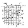
- FIG. 5 there is illustrated a layout or topological view of a portion of a semiconductor chip or wafer 46 in which the circuit of Fig. 4 is fabricated.
- the chip 46 includes a substrate 48 which may be made of P conductivity type silicon.
- An N well 50 is formed in the substrate 48 by, e.g., diffusion or implantation of arsenic.
- a first thin layer of silicon dioxide 52 is grown or deposited over the N well 50 and a second thin layer of silicon dioxide 54 is grown or deposited over substrate 48 outside of the N well 50 but adjacent thereto.
- a thick oxide layer 56 is grown or deposited by any known technique over the substrate 48 outside of the thin silicon dioxide layers 52 and 54.
- a plurality of parallely arranged conductive strips 58 are formed over the insulating layers 52, 54 and 56.
- a source/drain P conductivity type region 60 which may be made by implanting boron into N well 50 with the strips 58 acting as a shield for defining the channel regions of the PMOS devices or transistors, each of which includes two adjacent source/drain regions 60 separated by one of the strips 58 disposed over the transistor's channel region.
- a source/drain N conductivity type region 62 which may be made by implanting arsenic into the substrate 48 with the strips 58 acting as a shield for defining the channel regions of the NMOS devices or transistors, each of which includes two adjacent source/drain regions 62 separated by one of the strips 58 disposed over the transistor's channel region.
- a bus V H which may be made of metal, such as aluminum, and which is the source of potential for the logic circuit on chip 46 is formed over the P channel transistors 58, 60 and insulated from the polysilicon strips 58.
- a ground bus G which also may be made of metal is formed over the N channel transistors 58, 62 and insulated from the polysilicon strips 58.
- Metallic interconnecting strips 64 are also formed over the P and N channel transistors and are insulated from the polysilicon strips 58. Contacts to the source/drain regions 60 and 62 from the metal buses V H and G and the metallic strips 64 are indicated by an X.
- the transistors, including the control gates, of the logic circuit of Fig. 4 are indicated in Fig. 5 by the same reference characters.
- CMOS logic circuit forms a very compact CMOS logic circuit which is readily expandible and which adheres to an automated logic methodology. It is apparent that a finite matrix can be used as a program logic array which is programmable at the mask level. This implementation may be used for any CMOS technology.
- CMOS circuits also applies to static and dynamic NMOS circuits and to dynamic CMOS circuits.
- static NMOS circuits the P channel array or PMOS switch 10 is replaced by, e.g., a single N channel load device or transistor. Stacking is limited in this case due to ratioed constraints.
- Dynamic NMOS and CMOS circuits replace the P channel array 10 with pulsed or clocked load devices of either N or P channel type. Such arrays, however, are leakage and noise sensitive, and must be operated synchronously.
- the matrix 10 of Fig. 4 provides amplification, a full supply voltage being available at the output terminal Q. Additional amplification may be provided in the matrix if desired, to further improve speed.
Landscapes
- Engineering & Computer Science (AREA)
- Power Engineering (AREA)
- Physics & Mathematics (AREA)
- Computer Hardware Design (AREA)
- Computing Systems (AREA)
- General Engineering & Computer Science (AREA)
- Mathematical Physics (AREA)
- Logic Circuits (AREA)
- Metal-Oxide And Bipolar Metal-Oxide Semiconductor Integrated Circuits (AREA)
- Design And Manufacture Of Integrated Circuits (AREA)
Claims (8)
- Méthode de conception d'un circuit logique qui répond aux conditions d'une table de vérité ayant un nombre donné de symboles d'entrée binaires et de valeurs de sortie binaires, qui comprend les opérations suivantes :
formation d'entrées de premiers et deuxièmes termes de produit d'une première fonction boléenne (QP) à partir d'une table de vérité par complémentation des symboles d'entrée binaires qui sont un "1" lorsque la valeur de sortie est une valeur binaire "1" et utilisation du symbole d'entrée binaire vrai qui est un "0" lorsque la valeur de sortie est une valeur binaire "1" par constitution de premiers et deuxièmes circuits en série comprenant respectivement une pluralité de transistors à canal P et connexion de ces circuits en parallèle entre une source de tension et une borne de sortie, et par application d'une tension représentative de chaque entrée desdits premiers et deuxièmes termes de produit de la dite première fonction booléenne aux grilles de commande de ladite pluralité de transistors à canal P,
formation d'entrées de premiers et deuxièmes termes de produit d'une deuxième fonction boléenne (QN) à partir de ladite table de vérité par complémentation des symboles d'entrée binaires qui sont un "0" lorsque la valeur de sortie est une valeur binaire "0" et utilisation du symbole d'entrée binaire vrai qui est un "1" lorsque la valeur de sortie est une valeur binaire "0", par constitution de troisièmes et quatrièmes circuits en série comprenant respectivement une pluralité de transistors à canal N et connexion de ces circuits en parallèle entre ladite borne de sortie et un point de potentiel de référence, et par application d'une tension représentative de chaque entrée des dits premiers et deuxièmes termes de produit de ladite deuxième fonction boléenne aux grilles de commande de ladite pluralité de transistors à canal N. - Méthode suivant la revendication 1, caractérisée en ce qu'une desdites entrées formées est commune aux premiers et deuxièmes termes de ladite première fonction booléenne et en ce que, pour lesdits premiers et deuxièmes circuits en série, un transistor commun à canal P est formé .
- Méthode suivant la revendication 1, caractérisée en ce qu'une desdites entrées est commune aux premiers et deuxièmes termes de ladite deuxième fonction booléenne et en ce que, pour lesdits troisièmes et quatrièmes circuits en série, un transistor commun à canal P est formé.
- Méthode suivant la revendication 1, caractérisée par
une tension représentative de chaque entrée de chaque terme de produit de ladite première fonction booléenne qui est appliquée aux grilles de commande d'une pluralité de transistors à canal P qui sont interconnectés pour former une pluralité de circuits en série,
la connexion de ladite pluralité de circuits en série en un agencement parallèle entre une source de tension et une borne de sortie,
l'application d'une tension représentative de chaque entrée de chaque terme de produit de ladite deuxième fonction booléenne aux grilles de commande d'une pluralité de transistors à canal N interconnectés pour former une pluralité de circuits en série, et
la connexion de ladite pluralité de circuits en série de transistors à canal N en un agencement parallèle entre ladite borne de sortie et un point de potentiel de référence. - Méthode suivant la revendication 4, caractérisée par
la formation d'une première matrice (10) d'une pluralité de transistors à effet de champ à canal P et
la formation d'une deuxième matrice (12) d'une pluralité de transistors à effet de champ à canal N,
de sorte qu'une des entrées est commune à deux desdits termes de produit de ladite première fonction booléenne et au moins deux des circuits en série de transistors à canal P ou N ont un transistor commun à canal P ou N respectivement. - Méthode de conception d'un circuit logique suivant les revendications 1 ou 4,
caractérisée par
la formation de la première fonction booléenne QP en une forme ayant un nombre minimal d'entrées ;
la formation des entrées d'une pluralité de termes de produit d'une deuxième fonction booléenne QN à partir de ladite table de vérité par complémentation des symboles d'entrée binaires qui sont un "0" lorsque la valeur de sortie est une valeur binaire "0" et utilisation des symboles d'entrée binaires vrais qui sont un "1" lorsque la valeur de sortie est une valeur binaire "0",
la réduction de ladite deuxième fonction booléenne QN en une forme ayant un nombre minimal d'entrées ;
l'application d'une tension représentative de chacune dudit nombre minimal d'entrées de ladite première fonction booléenne QP aux grilles de commande d'une pluralité de transistors à canal P interconnectés pour former une pluralité de circuits en série,
la connexion de la pluralité de circuits en série en un agencement parallèle entre une source de tension et une borne de sortie,
l'application d'une tension représentative de chacune dudit nombre minimal d'entrées de ladite deuxième fonction booléenne QN aux grilles de commande d'une pluralité de transistors à canal N interconnectés pour former une pluralité de circuits en série, et
la connexion de la pluralité de circuits en série de transistors à canal N en un agencement parallèle entre ladite borne de sortie et un point de potentiel de référence. - Méthode suivant la revendication 5, caractérisée par
la formation de ladite deuxième matrice (12) de transistors à canal N dans une première région d'un substrat semi-conducteur de conductivité de type P,
la formation d'un puits N dans une deuxième région dudit substrat adjacente à ladite première région, et
la formation de ladite première matrice (10) de régions de canal P dans ledit puits N. - Méthode de conception d'un circuit logique suivant la revendication 6,
caractérisée par la formation d'une pluralité de circuits en série de transistors à canal P, en parallèle entre une source de tension et une borne de sortie,
l'application d'une tension représentative de chaque entrée de chaque terme de produit de ladite première fonction réduite aux grilles de commande des transistors à canal P d'un circuit respectif desdits circuits en série,
la formation d'une deuxième fonction ayant une pluralité de termes de produit à partir de ladite table de vérité, chacun desdits termes ayant un nombre d'entrées égal audit nombre donné et étant formé par complémentation des symboles d'entrée binaires qui sont un "0" lorsque la valeur de sortie est une valeur binaire "0" et utilisation du symbole d'entrée binaire vrai qui est un "1" lorsque la valeur de sortie est un "0",
la réduction de ladite deuxième fonction en une forme ayant un nombre minimal de termes de produit,
la formation d'une pluralité de circuits en série de transistors à canal N, en parallèle entre un point de potentiel de référence et ladite borne de sortie, et
l'application d'une tension représentative de chaque terme de produit de ladite deuxième fonction réduite aux grilles de commande des transistors à canal N d'un circuit respectif desdits circuits en série de transistors à canal N.
Applications Claiming Priority (2)
| Application Number | Priority Date | Filing Date | Title |
|---|---|---|---|
| US06/554,148 US4591993A (en) | 1983-11-21 | 1983-11-21 | Methodology for making logic circuits |
| US554148 | 1983-11-21 |
Publications (3)
| Publication Number | Publication Date |
|---|---|
| EP0142766A2 EP0142766A2 (fr) | 1985-05-29 |
| EP0142766A3 EP0142766A3 (en) | 1986-07-23 |
| EP0142766B1 true EP0142766B1 (fr) | 1991-09-25 |
Family
ID=24212228
Family Applications (1)
| Application Number | Title | Priority Date | Filing Date |
|---|---|---|---|
| EP84113322A Expired - Lifetime EP0142766B1 (fr) | 1983-11-21 | 1984-11-06 | Méthode de realisation de circuits logiques |
Country Status (4)
| Country | Link |
|---|---|
| US (1) | US4591993A (fr) |
| EP (1) | EP0142766B1 (fr) |
| JP (1) | JPS60117757A (fr) |
| DE (1) | DE3485112D1 (fr) |
Families Citing this family (26)
| Publication number | Priority date | Publication date | Assignee | Title |
|---|---|---|---|---|
| US4703435A (en) * | 1984-07-16 | 1987-10-27 | International Business Machines Corporation | Logic Synthesizer |
| US4700316A (en) * | 1985-03-01 | 1987-10-13 | International Business Machines Corporation | Automated book layout in static CMOS |
| JPH0668756B2 (ja) * | 1985-04-19 | 1994-08-31 | 株式会社日立製作所 | 回路自動変換方法 |
| US4792909A (en) * | 1986-04-07 | 1988-12-20 | Xerox Corporation | Boolean logic layout generator |
| US4745084A (en) * | 1986-11-12 | 1988-05-17 | Vlsi Technology, Inc. | Method of making a customized semiconductor integrated device |
| US4782249A (en) * | 1987-08-03 | 1988-11-01 | General Electric Company | Static CMOS programmable logic array |
| US5119313A (en) * | 1987-08-04 | 1992-06-02 | Texas Instruments Incorporated | Comprehensive logic circuit layout system |
| US5150309A (en) * | 1987-08-04 | 1992-09-22 | Texas Instruments Incorporated | Comprehensive logic circuit layout system |
| US4870598A (en) * | 1987-08-04 | 1989-09-26 | Texas Instruments Incorporated | Comprehensive logic circuit layout system |
| US4916627A (en) * | 1987-12-02 | 1990-04-10 | International Business Machines Corporation | Logic path length reduction using boolean minimization |
| US5173864A (en) * | 1988-08-20 | 1992-12-22 | Kabushiki Kaisha Toshiba | Standard cell and standard-cell-type integrated circuit |
| US4928160A (en) * | 1989-01-17 | 1990-05-22 | Ncr Corporation | Gate isolated base cell structure with off-grid gate polysilicon pattern |
| US4935646A (en) | 1989-02-22 | 1990-06-19 | International Business Machines Corporation | Fully static CMOS cascode voltage switch logic systems |
| US5243538B1 (en) * | 1989-08-09 | 1995-11-07 | Hitachi Ltd | Comparison and verification system for logic circuits and method thereof |
| US5237513A (en) * | 1989-11-20 | 1993-08-17 | Massachusetts Institute Of Technology | Optimal integrated circuit generation |
| US5084824A (en) * | 1990-03-29 | 1992-01-28 | National Semiconductor Corporation | Simulation model generation from a physical data base of a combinatorial circuit |
| US5313119A (en) * | 1991-03-18 | 1994-05-17 | Crosspoint Solutions, Inc. | Field programmable gate array |
| US5524082A (en) * | 1991-06-28 | 1996-06-04 | International Business Machines Corporation | Redundancy removal using quasi-algebraic methods |
| US5416719A (en) * | 1992-12-17 | 1995-05-16 | Vlsi Technology, Inc. | Computerized generation of truth tables for sequential and combinatorial cells |
| JP3182036B2 (ja) * | 1994-02-16 | 2001-07-03 | 松下電器産業株式会社 | 論理合成方法及び論理合成装置 |
| US5629636A (en) * | 1994-10-19 | 1997-05-13 | Crosspoint Solutions, Inc. | Ram-logic tile for field programmable gate arrays |
| US5465055A (en) * | 1994-10-19 | 1995-11-07 | Crosspoint Solutions, Inc. | RAM-logic tile for field programmable gate arrays |
| US6240542B1 (en) * | 1998-07-14 | 2001-05-29 | Lsi Logic Corporation | Poly routing for chip interconnects with minimal impact on chip performance |
| RU2171004C1 (ru) * | 2000-06-08 | 2001-07-20 | Шинкаренко Сергей Михайлович | Способ дифференциальной токовой защиты трехфазной электрической установки и устройство для его осуществления (варианты) |
| US7877711B2 (en) * | 2006-03-01 | 2011-01-25 | Nangate A/S | Methods of deriving switch networks |
| WO2008144330A1 (fr) * | 2007-05-15 | 2008-11-27 | Georgia Tech Research Corporation | Systèmes et procédés de formes booléennes améliorées |
Citations (1)
| Publication number | Priority date | Publication date | Assignee | Title |
|---|---|---|---|---|
| EP0130363A2 (fr) * | 1983-06-27 | 1985-01-09 | International Business Machines Corporation | Circuit logique différentiel réalisé en technologie à transistors complémentaires |
Family Cites Families (7)
| Publication number | Priority date | Publication date | Assignee | Title |
|---|---|---|---|---|
| US3252011A (en) * | 1964-03-16 | 1966-05-17 | Rca Corp | Logic circuit employing transistor means whereby steady state power dissipation is minimized |
| US3643232A (en) * | 1967-06-05 | 1972-02-15 | Texas Instruments Inc | Large-scale integration of electronic systems in microminiature form |
| NL176029C (nl) * | 1973-02-01 | 1985-02-01 | Philips Nv | Geintegreerde logische schakeling met komplementaire transistoren. |
| JPS5620734B2 (fr) * | 1973-07-31 | 1981-05-15 | ||
| JPS5244551A (en) * | 1975-10-06 | 1977-04-07 | Toshiba Corp | Logic circuit |
| US4356504A (en) * | 1980-03-28 | 1982-10-26 | International Microcircuits, Inc. | MOS Integrated circuit structure for discretionary interconnection |
| US4482810A (en) * | 1982-09-30 | 1984-11-13 | Storage Technology Partners | Electron beam exposure system |
-
1983
- 1983-11-21 US US06/554,148 patent/US4591993A/en not_active Expired - Lifetime
-
1984
- 1984-07-20 JP JP59149812A patent/JPS60117757A/ja active Granted
- 1984-11-06 EP EP84113322A patent/EP0142766B1/fr not_active Expired - Lifetime
- 1984-11-06 DE DE8484113322T patent/DE3485112D1/de not_active Expired - Lifetime
Patent Citations (1)
| Publication number | Priority date | Publication date | Assignee | Title |
|---|---|---|---|---|
| EP0130363A2 (fr) * | 1983-06-27 | 1985-01-09 | International Business Machines Corporation | Circuit logique différentiel réalisé en technologie à transistors complémentaires |
Non-Patent Citations (1)
| Title |
|---|
| Electro/80 Conference Record, May 13 - 15, 1980, Boston MA, Vol.5, p. 1-7 * |
Also Published As
| Publication number | Publication date |
|---|---|
| EP0142766A3 (en) | 1986-07-23 |
| JPH0544853B2 (fr) | 1993-07-07 |
| DE3485112D1 (de) | 1991-10-31 |
| JPS60117757A (ja) | 1985-06-25 |
| EP0142766A2 (fr) | 1985-05-29 |
| US4591993A (en) | 1986-05-27 |
Similar Documents
| Publication | Publication Date | Title |
|---|---|---|
| EP0142766B1 (fr) | Méthode de realisation de circuits logiques | |
| US7466163B2 (en) | Look-up table structure with embedded carry logic | |
| US7239174B2 (en) | Programmable interconnect structures | |
| US7285984B2 (en) | Look-up table structure with embedded carry logic | |
| US4737837A (en) | Ring topology for an integrated circuit logic cell | |
| US20060132175A1 (en) | Look-up table based logic macro-cells | |
| KR890003147B1 (ko) | 게이트 에레이 | |
| US5671397A (en) | Sea-of-cells array of transistors | |
| EP0528956A1 (fr) | CELLULE DE BASE POUR RESEAU DE PORTES BiCMOS | |
| EP0809362A2 (fr) | Circuit logique et sa méthode de fabrication | |
| US20070171105A1 (en) | Look-up table structure with embedded carry logic | |
| US4862241A (en) | Semiconductor integrated circuit device | |
| EP0290857B1 (fr) | Dispositif de polarisation de grille pour réaliser une capacitance indépendante de la tension | |
| US4833347A (en) | Charge disturbance resistant logic circuits utilizing true and complement input control circuits | |
| CA1241115A (fr) | Tracage automatique de circuits logiques a commutateurs de tension en cascode | |
| US5814846A (en) | Cell apparatus and method for use in building complex integrated circuit devices | |
| EP0092176B1 (fr) | Cellule de base pour réseau de portes à circuit intégré | |
| US4566022A (en) | Flexible/compressed array macro design | |
| US4652777A (en) | CMOS programmable logic array | |
| US4880754A (en) | Method for providing engineering changes to LSI PLAs | |
| WU et al. | Invited paper A unified theory for MOS circuit design—switching network logic | |
| US4952824A (en) | Ion implantation programmable logic device | |
| CN1202739A (zh) | 半导体器件 | |
| US5701021A (en) | Cell architecture for mixed signal applications | |
| EP1723723B1 (fr) | Cellule de base logique, ensemble cellules de base logiques et dispositif logique |
Legal Events
| Date | Code | Title | Description |
|---|---|---|---|
| PUAI | Public reference made under article 153(3) epc to a published international application that has entered the european phase |
Free format text: ORIGINAL CODE: 0009012 |
|
| 17P | Request for examination filed |
Effective date: 19841211 |
|
| AK | Designated contracting states |
Designated state(s): DE FR GB |
|
| PUAL | Search report despatched |
Free format text: ORIGINAL CODE: 0009013 |
|
| RHK1 | Main classification (correction) |
Ipc: H03K 19/173 |
|
| AK | Designated contracting states |
Kind code of ref document: A3 Designated state(s): DE FR GB |
|
| 17Q | First examination report despatched |
Effective date: 19871120 |
|
| GRAA | (expected) grant |
Free format text: ORIGINAL CODE: 0009210 |
|
| AK | Designated contracting states |
Kind code of ref document: B1 Designated state(s): DE FR GB |
|
| REF | Corresponds to: |
Ref document number: 3485112 Country of ref document: DE Date of ref document: 19911031 |
|
| ET | Fr: translation filed | ||
| PLBE | No opposition filed within time limit |
Free format text: ORIGINAL CODE: 0009261 |
|
| STAA | Information on the status of an ep patent application or granted ep patent |
Free format text: STATUS: NO OPPOSITION FILED WITHIN TIME LIMIT |
|
| 26N | No opposition filed | ||
| PGFP | Annual fee paid to national office [announced via postgrant information from national office to epo] |
Ref country code: GB Payment date: 19941013 Year of fee payment: 11 |
|
| PGFP | Annual fee paid to national office [announced via postgrant information from national office to epo] |
Ref country code: FR Payment date: 19941103 Year of fee payment: 11 |
|
| PGFP | Annual fee paid to national office [announced via postgrant information from national office to epo] |
Ref country code: DE Payment date: 19941201 Year of fee payment: 11 |
|
| PG25 | Lapsed in a contracting state [announced via postgrant information from national office to epo] |
Ref country code: GB Effective date: 19951106 |
|
| GBPC | Gb: european patent ceased through non-payment of renewal fee |
Effective date: 19951106 |
|
| PG25 | Lapsed in a contracting state [announced via postgrant information from national office to epo] |
Ref country code: FR Effective date: 19960731 |
|
| PG25 | Lapsed in a contracting state [announced via postgrant information from national office to epo] |
Ref country code: DE Effective date: 19960801 |
|
| REG | Reference to a national code |
Ref country code: FR Ref legal event code: ST |