EP0143040B1 - Optische Vorrichtung zur Konzentration der Lichtstrahlung einer LED, und mit dieser Vorrichtung versehene LED - Google Patents
Optische Vorrichtung zur Konzentration der Lichtstrahlung einer LED, und mit dieser Vorrichtung versehene LED Download PDFInfo
- Publication number
- EP0143040B1 EP0143040B1 EP84402179A EP84402179A EP0143040B1 EP 0143040 B1 EP0143040 B1 EP 0143040B1 EP 84402179 A EP84402179 A EP 84402179A EP 84402179 A EP84402179 A EP 84402179A EP 0143040 B1 EP0143040 B1 EP 0143040B1
- Authority
- EP
- European Patent Office
- Prior art keywords
- lens
- diode
- emitting diode
- light
- lenses
- Prior art date
- Legal status (The legal status is an assumption and is not a legal conclusion. Google has not performed a legal analysis and makes no representation as to the accuracy of the status listed.)
- Expired
Links
Images

Classifications
-
- H—ELECTRICITY
- H10—SEMICONDUCTOR DEVICES; ELECTRIC SOLID-STATE DEVICES NOT OTHERWISE PROVIDED FOR
- H10H—INORGANIC LIGHT-EMITTING SEMICONDUCTOR DEVICES HAVING POTENTIAL BARRIERS
- H10H20/00—Individual inorganic light-emitting semiconductor devices having potential barriers, e.g. light-emitting diodes [LED]
- H10H20/80—Constructional details
- H10H20/81—Bodies
- H10H20/813—Bodies having a plurality of light-emitting regions, e.g. multi-junction LEDs or light-emitting devices having photoluminescent regions within the bodies
-
- G—PHYSICS
- G02—OPTICS
- G02B—OPTICAL ELEMENTS, SYSTEMS OR APPARATUS
- G02B6/00—Light guides; Structural details of arrangements comprising light guides and other optical elements, e.g. couplings
- G02B6/24—Coupling light guides
- G02B6/42—Coupling light guides with opto-electronic elements
- G02B6/4298—Coupling light guides with opto-electronic elements coupling with non-coherent light sources and/or radiation detectors, e.g. lamps, incandescent bulbs, scintillation chambers
-
- H—ELECTRICITY
- H10—SEMICONDUCTOR DEVICES; ELECTRIC SOLID-STATE DEVICES NOT OTHERWISE PROVIDED FOR
- H10H—INORGANIC LIGHT-EMITTING SEMICONDUCTOR DEVICES HAVING POTENTIAL BARRIERS
- H10H20/00—Individual inorganic light-emitting semiconductor devices having potential barriers, e.g. light-emitting diodes [LED]
- H10H20/80—Constructional details
- H10H20/81—Bodies
- H10H20/819—Bodies characterised by their shape, e.g. curved or truncated substrates
-
- G—PHYSICS
- G02—OPTICS
- G02B—OPTICAL ELEMENTS, SYSTEMS OR APPARATUS
- G02B6/00—Light guides; Structural details of arrangements comprising light guides and other optical elements, e.g. couplings
- G02B6/24—Coupling light guides
- G02B6/42—Coupling light guides with opto-electronic elements
- G02B6/4201—Packages, e.g. shape, construction, internal or external details
- G02B6/4204—Packages, e.g. shape, construction, internal or external details the coupling comprising intermediate optical elements, e.g. lenses, holograms
- G02B6/4206—Optical features
-
- H—ELECTRICITY
- H10—SEMICONDUCTOR DEVICES; ELECTRIC SOLID-STATE DEVICES NOT OTHERWISE PROVIDED FOR
- H10H—INORGANIC LIGHT-EMITTING SEMICONDUCTOR DEVICES HAVING POTENTIAL BARRIERS
- H10H20/00—Individual inorganic light-emitting semiconductor devices having potential barriers, e.g. light-emitting diodes [LED]
- H10H20/80—Constructional details
- H10H20/81—Bodies
- H10H20/819—Bodies characterised by their shape, e.g. curved or truncated substrates
- H10H20/821—Bodies characterised by their shape, e.g. curved or truncated substrates of the light-emitting regions, e.g. non-planar junctions
-
- H—ELECTRICITY
- H10—SEMICONDUCTOR DEVICES; ELECTRIC SOLID-STATE DEVICES NOT OTHERWISE PROVIDED FOR
- H10H—INORGANIC LIGHT-EMITTING SEMICONDUCTOR DEVICES HAVING POTENTIAL BARRIERS
- H10H20/00—Individual inorganic light-emitting semiconductor devices having potential barriers, e.g. light-emitting diodes [LED]
- H10H20/80—Constructional details
- H10H20/85—Packages
- H10H20/855—Optical field-shaping means, e.g. lenses
Definitions
- the present invention relates to an optical device for concentrating the light emitted by a light-emitting diode, this device being integrated into the light-emitting diode, and produced in one of the layers of semiconductor material constituting the diode. It is characterized in that it comprises, on the surface of the diode, at least one half-toroid lens, surrounding a central lens, said torus forming a complete ring in the plane of the surface of the diode, and being cut in the sense of its thickness.
- the invention also relates to the light-emitting diode with which this optical device is associated.
- the invention applies to light-emitting diodes in general, which are of the type with emission from above, that is to say by the face opposite to the substrate, better known by their English name “top emitting”, or whatever. are of the “Burrus” type, that is to say emission through an excessively formed in the substrate, the diode being inverted with respect to its substrate, and welded to its base by its epitaxial layers, and no longer, as this is the general case, by its substrate. This is why the internal structure of the diode will not be detailed in the description of the invention, since it is not concerned with the invention.
- the invention applies to light-emitting diodes made from materials of the 111-V family and in particular alloys based on gallium and arsenic, such as Ga As and Ga x Al i - x Aces which are the most common, without being limiting.
- the problem to which the invention provides a solution is that of optical coupling between a light-emitting diode and an optical fiber, for all telecommunications, computer or office automation installations using fiber interfaces.
- the effective solution to this problem of power loss consists in fitting an exit lens to the surface of the diode.
- the adaptation of the indices of the different media, and the shape of the optics make it possible to recover a larger quantity of light emitted by the active layer of the light-emitting diode.
- one of the problems is that of the dimensions of the optical device adapted to the diode. Limiting the thickness of the layers that can be epitaxied limits the radius of the lenses that can be cut in these layers, and therefore the amount of light recovered by each. lens: a large diameter lens recovers more light but requires a thick layer, but it is not possible to make layers greater than 20 ⁇ m thick. To obtain a more intense light beam at the end of the optical fiber, it has been proposed to combine several lenses side by side, corresponding to as many emissive zones in the body of the diode. But the association of circular lenses is not optimal: in the upper plane of the diode, the plane in which the lenses are attached, a large fraction of the surface is not used, in the form of curvilinear triangles inserted between the lenses.
- a light-emitting diode comprises, on the surface through which the light exits, a central hemispherical lens and, surrounding the latter, at least one second plano-convex lens in the shape of a torus, this torus being cut along a parallel plane in the plane of the surface through which the light comes out.
- the area occupied by the optical device is better, compared to the area of the diode, and the unused areas are limited to the guard distances between lenses, necessary during the manufacture of said lenses.
- the light emitting diode associated with such an optical device comprises either a single emissive zone, covered by the central lens and the toric lenses, or a central emissive zone corresponding to the central lens, and as many emissive zones in the form of a ring as it there are toroid lenses.
- the invention relates to an optical device for concentrating the light radiation emitted by a light-emitting diode; comprising at least one emissive zone defined in the active layer of said diode, a hemispherical lens, centered with respect to the emissive zone and produced in the contact layer which supports an electrical contact metallization and which is made of a semi-material conductor transparent to the wavelength of the radiation emitted by the diode and at least one plano-convex hemitoric lens, concentric with the central hemispherical lens.
- Figure 1 shows a sectional view of a light emitting diode emitting from the upper face (top emitting) provided with a lens, as described for example in EP-A-0 101 368 filed by the applicant.
- Such a light-emitting diode comprises what will subsequently be called the body of the diode, and the precise detail of which does not need to be given since it is outside the scope of the invention.
- This body comprises at least one substrate 1 and an emissive zone 2 included in an active layer 3, delimited by two confinement layers 4 and 5.
- ohmic 7 which makes it possible to apply a voltage to the light-emitting diode, the other contact 8 being taken on the substrate.
- a lens 9 which allows to recover the light rays from the emissive area 2, so as to increase the optical power transmitted to the optical fiber not shown in this figure, but which is close to the lens 9.
- Light rays such as L1 which are orthogonal to the exit plane of the light-emitting diode are transmitted without difficulty.
- the dimensions of the optics that is to say the radius of the lens 9, must be substantial to ensure a sufficient gain in power without excessively increasing the operating current of the component, since the increase in the current density in the emissive zone 2 heats the light-emitting diode. Therefore, the layer of material, in which the optics must be etched, must be thick, so as to be able to etch a lens 9 of large radius.
- the solution presented in FIG. 2 therefore has the advantage of requiring only one possible thickness of the last layer for manufacturing the diode, that is to say a thickness in which it is still possible to cut lenses 91 to 94: a few tens of micrometers easily achievable by epitaxy.
- this layer is etched by a collective and well controllable method the series of relatively small diameter surface lenses allowing the transfer of light to an optical fiber.
- the idea which presides over the production of a light-emitting diode according to FIG. 2 is therefore the homogeneous distribution of the emitting zone into several small elementary zones 21, 22, 23 and 24, so as to integrate more easily above each. from it a lens etched directly into the structure, by a collective machining technique.
- This idea applies to surface emitting diodes of the top emitting type or to “Burrus” diodes.
- the "Burrus" diode has a definite advantage over the top emitting diode: its better cooling. Welded on its support by the side of the epitaxial layers, heat dissipation takes place more easily towards the housing in a “Burrus” diode than in the case of a top-emitting diode.
- FIG. 3 which represents a plan view of FIG. 2, shows the arrangement of the lenses in the light-emitting diode and will make it easier to understand that this system is not yet optimized.
- the surface occupied by 7 elementary lenses of radius R / 3, inside a circle of radius R is equal to 78% of the surface of the large circle: we can therefore only recover a maximum of 78% of the light emitted by the diode, if it is admitted that this light leaves by all its upper surface.
- a simple calculation leads to the following result: the 7 elementary lenses occupy 336/900 of the surface of the circle T rR 2 , or the presence of the guard g necessary for the production of the elementary lenses lowers the yield or the density of the lenses on the surface of the diode at 37.42% of the possible area.
- the limitation of the surface of elementary lenses such as 91 leads to working with high injection densities by emissive areas such as 21, so as to obtain more light power, but leads to heating of the light emitting diode.
- FIG. 4 represents a first step, corresponding to the development of the invention.
- this substrate it is possible to write a circle 10 of radius R of the same dimension as that defined in FIG. 3, this circle entering inside the contacting metallization 7 which is necessarily deposited on the surface of a light emitting diode. But instead of making circular emissive zones such as 21, 22 ...
- the light-emitting diode comprises at least one emissive zone in the form of a ribbon and a lens having a radius of curvature finished in a plane orthogonal to the ribbon of the emissive zone, and an infinite radius of curvature in a plane tangent to the same ribbon.
- the semi-cylindrical lenses are a first case, and the semi-cylindrical lenses 11, 12, 13, 14 cover the largest possible area of the area available inside the metallization of the contact. 7.
- To these cylindrical lenses correspond emissive zones 15, 16, 17, 18 produced in the active layer of the light-emitting diode, these emissive zones being centered with respect to cylindrical lenses 11, 12, 13 ...
- Such an arrangement makes it possible to occupy a much larger area on the surface of the body of the light-emitting diode, since it suffices to have a guard space between each of the cylindrical lenses, but there is no longer the equivalent of the curvilinear triangles described in FIG. 3.
- the emissive zones 15, 16, 17, 18 having in total a greater surface area than the circular emissive zones such as 21, a lower surface injection density than in the previous case of circular lenses allow less heating of the light emitting diode.
- a third light ray L3, emitted by the emissive element 15 in a plane P3 parallel to the main axis of the semi-cylindrical lens 11 can be recovered in the direction of the optical fiber, if its angle of incidence is less than 16 ° 4 'but can also be lost if, as shown in Figure 5, it is too oblique and has an angle of incidence, on the surface of the semi-cylindrical lens, greater than 16 ° 4'.
- Such an arrangement based on semi-cylindrical lenses therefore makes it possible to recover more useful surface on the surface of the diode, and also makes it possible to have emissive zones 15, 16 ... which work under a lower injection density to obtain the same light emission.
- this geometry does not avoid losing part of the radiation which is reflected along the main axis of the lenses, as is the case for the radius L3 in FIG. 5.
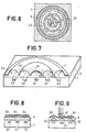
- FIG. 6 represents a plan view of the upper surface of a light-emitting diode provided with the optical device according to the invention.
- the upper layer of this light-emitting diode are cut at least one central hemispherical lens 31 and at least one semitonic lens 32, concentric with the central lens 31.
- semitoric lens 32 it should be understood that the lens 32 forms a complete circle around the central lens 31, but that it is not, seen in section and in the thickness direction, that a fraction of a torus since a torus is by definition generated by a circle moving around a point which is external to it.
- the semi-toric lens 32 therefore has, as will be shown in FIG. 7, a section in a plane perpendicular to the main plane of the light-emitting diode which is a fraction of a circle.
- An emissive zone is associated with each of the lenses constituting the optical device of the light-emitting diode: the emissive zone 41 corresponding to the circular central lens 31 is itself a circular emissive zone, while the emissive zone 42 corresponding to the semi-objective lens O-ring 32 is itself an emissive zone in the form of a ribbon forming a circle.
- all the emissive areas that is to say the emissive area 41 in the center of the light-emitting diode and the emissive ring 42, or the rings if there is a plurality of lenses in half toroid on the diode, have a total surface much larger than in the case shown in Figures 2 and 3, that is to say localized emissive areas. This makes it possible to reduce the density of current injection into the diode and therefore to limit the heating.
- FIG. 7 represents a three-quarter view in space of a light-emitting diode provided with an optical device according to the invention. This view makes it easier to highlight the structure, because it provides the relief that is missing in Figure 6.
- the body 1 of the diode is not detailed: it is understood that this body comprises at least one substrate, and at least one active layer comprised between two confinement layers, as well as the metallizations necessary for setting on the diode. Only the emissive zones 41, 42 and 43 have been shown, since, by way of nonlimiting example, FIG. 7 represents a diode provided with two semi-toric lenses.
- the central emissive zone 41 is a circle, and the emissive zones 42 and 43 are rings.
- the central lens 31 and the two semi-toric lenses 32 and 33 have in this figure a section which is substantially that of a semicircle.
- This is only an embodiment of a diode provided with the optical device of the invention because the convexity of the central lens and of the semi-toric lenses is defined by the environmental conditions, it is ie the distance between an emissive region such as 41 and the lens associated therewith 31 on the one hand, and the distance between said lens 31 and the optical fiber on the other hand. Consequently, the lenses making up the system according to the invention may have a curvature which is limited to a fraction of a circle, less than the semicircle.
- the maximum efficiency of the device is obtained for lenses the diameter of which, for the central lens 31, or the width, for the toric lenses 32 and 33, is approximately four times the width of the emitter tape 41 or 42.
- the dimensions of the convergence optics are also linked to the radius of curvature r of each of the lenses, this radius being limited by the thickness of the epitaxial layers that can currently be produced, that is to say a maximum of 25 ⁇ m approximately in materials of the Ga AI As type, and under conditions suitable for making good optics.
- FIG. 8 represents, very schematically, the body 1 of a light-emitting diode as well as the emissive zones 41 and 42.
- the diode structure having already received the different confinement layers, active and other layers in detail of which it is not no need to enter, since they are outside the scope of the invention, a thick layer 6 is deposited on the surface of the diode opposite that of the substrate.
- This thick layer 6 must necessarily be made of a material transparent to the wavelength of the light emitted by the diode: if the diode is based on Ga As and Ga AI As, layer 6 will necessarily include aluminum for be transparent.
- This layer can be produced by different techniques, some of which are not advantageous from the point of view of speed of production and economy, others being more particularly recommended such as liquid epitaxy or organometallic epitaxy.
- a layer of masking resin which is then etched so as to give an imprint 51, which corresponds to the future central circular lens 31, and at least one imprint in the form of a ring 52, which corresponds to the future first semi-toric lens 32.
- FIG. 9 represents the next step in producing the optics.
- the islands 51 and 52 of resin deform and, by the voltages ca pillar and by creep, they give islands 61 and 62 which are now in the form of a circular lens for the island 61 and a hemi-toric lens for the island 62.
- the islands 61 and 62 do not constitute the optics according to the invention but only the masks which make it possible to cut the optical device in the layer of semiconductor material 6 by ion machining.
- the organic masking resin erodes twice as slowly as the semiconductor material, under the impact of ions in the ion beam.
- the layer 6 of crystalline material is therefore machined with a different speed depending on the thickness of the resin mask which is deposited on it: when the machining is finished, the central lens and the semi-toric lens (s) 31 and 32 are produced and they have been represented in this figure 9 in the form of dotted lines in layer 6.
- the description of the invention has been made based on the case where the optic comprises only one or two semi-toric lenses: of course this is only a simplification of the figures but the The invention applies to the case where a light-emitting diode, coupled to a device of larger size than an optical fiber, comprises a plurality of semi-toric lenses.
- the internal structure of the diode as a semiconductor device does not limit the scope of the invention which relates to an optical system for concentrating light rays, with a view to improving the efficiency of existing light emitting diodes.
- the invention is therefore clarified by the following claims.
Landscapes
- Physics & Mathematics (AREA)
- General Physics & Mathematics (AREA)
- Optics & Photonics (AREA)
- Led Devices (AREA)
- Led Device Packages (AREA)
- Optical Couplings Of Light Guides (AREA)
Claims (6)
Applications Claiming Priority (2)
| Application Number | Priority Date | Filing Date | Title |
|---|---|---|---|
| FR8317583A FR2554606B1 (fr) | 1983-11-04 | 1983-11-04 | Dispositif optique de concentration du rayonnement lumineux emis par une diode electroluminescente, et diode electroluminescente comportant un tel dispositif |
| FR8317583 | 1983-11-06 |
Publications (2)
| Publication Number | Publication Date |
|---|---|
| EP0143040A1 EP0143040A1 (de) | 1985-05-29 |
| EP0143040B1 true EP0143040B1 (de) | 1988-06-01 |
Family
ID=9293807
Family Applications (1)
| Application Number | Title | Priority Date | Filing Date |
|---|---|---|---|
| EP84402179A Expired EP0143040B1 (de) | 1983-11-04 | 1984-10-30 | Optische Vorrichtung zur Konzentration der Lichtstrahlung einer LED, und mit dieser Vorrichtung versehene LED |
Country Status (6)
| Country | Link |
|---|---|
| US (1) | US4703219A (de) |
| EP (1) | EP0143040B1 (de) |
| JP (1) | JPS60113979A (de) |
| CA (1) | CA1245331A (de) |
| DE (1) | DE3471835D1 (de) |
| FR (1) | FR2554606B1 (de) |
Families Citing this family (63)
| Publication number | Priority date | Publication date | Assignee | Title |
|---|---|---|---|---|
| FR2593930B1 (fr) * | 1986-01-24 | 1989-11-24 | Radiotechnique Compelec | Dispositif opto-electronique pour montage en surface |
| JP2532449B2 (ja) * | 1987-03-27 | 1996-09-11 | 株式会社日立製作所 | 半導体レ−ザ装置 |
| WO1991002391A1 (en) * | 1989-08-02 | 1991-02-21 | Australian Electro Optics Pty. Ltd. | A diode laser system emitting a high quality laser beam of circular cross-section perpendicular to the mounting base |
| US5051790A (en) * | 1989-12-22 | 1991-09-24 | David Sarnoff Research Center, Inc. | Optoelectronic interconnections for integrated circuits |
| US6590502B1 (en) | 1992-10-12 | 2003-07-08 | 911Ep, Inc. | Led warning signal light and movable support |
| JPH09307144A (ja) * | 1996-05-14 | 1997-11-28 | Matsushita Electric Ind Co Ltd | 発光素子及びその製造方法 |
| US6031958A (en) * | 1997-05-21 | 2000-02-29 | Mcgaffigan; Thomas H. | Optical light pipes with laser light appearance |
| GB2330679B (en) | 1997-10-21 | 2002-04-24 | 911 Emergency Products Inc | Warning signal light |
| US6525386B1 (en) | 1998-03-10 | 2003-02-25 | Masimo Corporation | Non-protruding optoelectronic lens |
| US6462669B1 (en) | 1999-04-06 | 2002-10-08 | E. P . Survivors Llc | Replaceable LED modules |
| US6380865B1 (en) | 1999-04-06 | 2002-04-30 | 911 Emergency Products, Inc. | Replacement led lamp assembly and modulated power intensity for light source |
| US6614359B2 (en) | 1999-04-06 | 2003-09-02 | 911 Emergency Products, Inc. | Replacement led lamp assembly and modulated power intensity for light source |
| US6700502B1 (en) | 1999-06-08 | 2004-03-02 | 911Ep, Inc. | Strip LED light assembly for motor vehicle |
| US6705745B1 (en) * | 1999-06-08 | 2004-03-16 | 911Ep, Inc. | Rotational led reflector |
| WO2000074972A1 (en) | 1999-06-08 | 2000-12-14 | 911 Emergency Products, Inc. | Led light stick assembly |
| US6623151B2 (en) | 1999-08-04 | 2003-09-23 | 911Ep, Inc. | LED double light bar and warning light signal |
| US6367949B1 (en) | 1999-08-04 | 2002-04-09 | 911 Emergency Products, Inc. | Par 36 LED utility lamp |
| US6547410B1 (en) | 2000-07-28 | 2003-04-15 | 911 Emergency Products, Inc. | LED alley/take-down light |
| WO2001095673A1 (en) | 2000-06-06 | 2001-12-13 | 911 Emergency Products, Inc. | Led compensation circuit |
| AUPQ818100A0 (en) * | 2000-06-15 | 2000-07-06 | Arlec Australia Limited | Led lamp |
| US7320632B2 (en) * | 2000-06-15 | 2008-01-22 | Lednium Pty Limited | Method of producing a lamp |
| US6570324B1 (en) * | 2000-07-19 | 2003-05-27 | Eastman Kodak Company | Image display device with array of lens-lets |
| US7439847B2 (en) * | 2002-08-23 | 2008-10-21 | John C. Pederson | Intelligent observation and identification database system |
| US8188878B2 (en) | 2000-11-15 | 2012-05-29 | Federal Law Enforcement Development Services, Inc. | LED light communication system |
| WO2002041276A2 (en) * | 2000-11-15 | 2002-05-23 | Snowy Village, Inc. | Led warning light and communication system |
| WO2002059983A1 (en) * | 2000-11-17 | 2002-08-01 | Emcore Corporation | Led package having improved light extraction and methods therefor |
| US6809470B2 (en) * | 2000-12-29 | 2004-10-26 | Intel Corporation | Flat panel color display with enhanced brightness and preferential viewing angles |
| US6946788B2 (en) * | 2001-05-29 | 2005-09-20 | Toyoda Gosei Co., Ltd. | Light-emitting element |
| CN1663044A (zh) * | 2002-06-14 | 2005-08-31 | 莱尼股份有限公司 | 灯和制灯方法 |
| JP4080843B2 (ja) | 2002-10-30 | 2008-04-23 | 株式会社東芝 | 不揮発性半導体記憶装置 |
| DE10303969B4 (de) * | 2003-01-31 | 2008-11-27 | Osram Opto Semiconductors Gmbh | Leuchtdiodenanordnung mit einem Leuchtdiodenträger und einer Mehrzahl von Leuchtdioden |
| CA2518625A1 (en) * | 2003-03-12 | 2004-09-23 | Lednium Pty. Ltd. | A lamp and a process for producing a lamp |
| WO2005001944A1 (ja) * | 2003-06-26 | 2005-01-06 | Nippon Sheet Glass Company, Limited | レンズ付き発光素子およびその製造方法 |
| JP4479357B2 (ja) * | 2003-06-26 | 2010-06-09 | 富士ゼロックス株式会社 | レンズ付き発光素子、レンズ付き発光素子アレイ、自己走査型発光素子アレイ、書込みヘッドおよび光プリンタ |
| CN100546056C (zh) * | 2003-06-26 | 2009-09-30 | 富士施乐株式会社 | 带有透镜的发光元件以及其制造方法 |
| JP4635494B2 (ja) * | 2004-07-13 | 2011-02-23 | 富士ゼロックス株式会社 | レンズ付き発光素子 |
| FR2874099B1 (fr) * | 2004-08-06 | 2006-10-13 | Thales Sa | Source d'eclairage pour afficheur a cristaux liquides |
| US7737459B2 (en) * | 2004-09-22 | 2010-06-15 | Cree, Inc. | High output group III nitride light emitting diodes |
| US7259402B2 (en) * | 2004-09-22 | 2007-08-21 | Cree, Inc. | High efficiency group III nitride-silicon carbide light emitting diode |
| US8174037B2 (en) | 2004-09-22 | 2012-05-08 | Cree, Inc. | High efficiency group III nitride LED with lenticular surface |
| US8513686B2 (en) * | 2004-09-22 | 2013-08-20 | Cree, Inc. | High output small area group III nitride LEDs |
| US8288942B2 (en) * | 2004-12-28 | 2012-10-16 | Cree, Inc. | High efficacy white LED |
| KR20070015345A (ko) * | 2005-07-30 | 2007-02-02 | 엘지마이크론 주식회사 | 면발광 램프와 이를 이용한 액정표시장치 |
| ES2265780B1 (es) * | 2005-08-04 | 2007-11-16 | Odeco Electronica, S.A. | Valla publicitaria electronica para pie de campo. |
| US7474465B2 (en) * | 2005-11-14 | 2009-01-06 | Motorola, Inc. | Electrically-responsive lenticular display apparatus and method |
| US8596819B2 (en) | 2006-05-31 | 2013-12-03 | Cree, Inc. | Lighting device and method of lighting |
| US11265082B2 (en) | 2007-05-24 | 2022-03-01 | Federal Law Enforcement Development Services, Inc. | LED light control assembly and system |
| US9294198B2 (en) | 2007-05-24 | 2016-03-22 | Federal Law Enforcement Development Services, Inc. | Pulsed light communication key |
| US9455783B2 (en) | 2013-05-06 | 2016-09-27 | Federal Law Enforcement Development Services, Inc. | Network security and variable pulse wave form with continuous communication |
| US9414458B2 (en) | 2007-05-24 | 2016-08-09 | Federal Law Enforcement Development Services, Inc. | LED light control assembly and system |
| WO2008148039A1 (en) | 2007-05-24 | 2008-12-04 | Federal Law Enforcement Development Services, Inc. | Led light communication system |
| US9258864B2 (en) | 2007-05-24 | 2016-02-09 | Federal Law Enforcement Development Services, Inc. | LED light control and management system |
| US9100124B2 (en) | 2007-05-24 | 2015-08-04 | Federal Law Enforcement Development Services, Inc. | LED Light Fixture |
| US8529441B2 (en) * | 2008-02-12 | 2013-09-10 | Innurvation, Inc. | Ingestible endoscopic optical scanning device |
| US8890773B1 (en) | 2009-04-01 | 2014-11-18 | Federal Law Enforcement Development Services, Inc. | Visible light transceiver glasses |
| CN102971875A (zh) * | 2010-08-09 | 2013-03-13 | 松下电器产业株式会社 | 半导体发光器件 |
| US8543505B2 (en) | 2011-01-14 | 2013-09-24 | Federal Law Enforcement Development Services, Inc. | Method of providing lumens and tracking of lumen consumption |
| US9265112B2 (en) | 2013-03-13 | 2016-02-16 | Federal Law Enforcement Development Services, Inc. | LED light control and management system |
| US9000467B2 (en) | 2013-07-11 | 2015-04-07 | Dong Yang CHIOU | Non-chip LED illumination device |
| CN103605192B (zh) * | 2013-11-29 | 2015-07-15 | 武汉光迅科技股份有限公司 | 一种光学耦合装置及其制作方法 |
| US20150198941A1 (en) | 2014-01-15 | 2015-07-16 | John C. Pederson | Cyber Life Electronic Networking and Commerce Operating Exchange |
| DE102015122627A1 (de) * | 2015-05-28 | 2016-12-01 | Osram Opto Semiconductors Gmbh | Optoelektronische Anordnung und Tiefenerfassungssystem |
| US20170046950A1 (en) | 2015-08-11 | 2017-02-16 | Federal Law Enforcement Development Services, Inc. | Function disabler device and system |
Family Cites Families (15)
| Publication number | Priority date | Publication date | Assignee | Title |
|---|---|---|---|---|
| US3414733A (en) * | 1965-02-15 | 1968-12-03 | Hewlett Packard Co | Annularly shaped light emitter and photocell connected by plug-in light conducting pad |
| US3523720A (en) * | 1968-07-09 | 1970-08-11 | Rollei Werke Franke Heidecke | Fresnel field lens for reflex cameras |
| US3812516A (en) * | 1970-05-01 | 1974-05-21 | Bell Telephone Labor Inc | Spontaneously emitting hetero-structure junction diodes |
| JPS5422115B2 (de) * | 1972-05-19 | 1979-08-04 | ||
| US3947840A (en) * | 1974-08-16 | 1976-03-30 | Monsanto Company | Integrated semiconductor light-emitting display array |
| CA1007736A (en) * | 1974-09-10 | 1977-03-29 | Northern Electric Company | Integral lens light emitting diode |
| US3954534A (en) * | 1974-10-29 | 1976-05-04 | Xerox Corporation | Method of forming light emitting diode array with dome geometry |
| US4079404A (en) * | 1976-12-30 | 1978-03-14 | International Business Machines Corporation | Self-aligning support structure for optical components |
| US4165474A (en) * | 1977-12-27 | 1979-08-21 | Texas Instruments Incorporated | Optoelectronic displays using uniformly spaced arrays of semi-sphere light-emitting diodes |
| US4275414A (en) * | 1979-01-04 | 1981-06-23 | Westinghouse Electric Corp. | Tube plug weld inspection apparatus |
| GB2046005B (en) * | 1979-03-29 | 1983-02-09 | Standard Telephones Cables Ltd | Injection laser devices |
| JPS5651884A (en) * | 1979-10-03 | 1981-05-09 | Hitachi Ltd | Light sending and recieving element |
| US4467193A (en) * | 1981-09-14 | 1984-08-21 | Carroll Manufacturing Corporation | Parabolic light emitter and detector unit |
| US4599537A (en) * | 1982-04-30 | 1986-07-08 | Shigeaki Yamashita | IR light emitting apparatus with visible detection means |
| FR2531814B1 (fr) * | 1982-08-10 | 1986-04-11 | Thomson Csf | Association monolithique de diodes electroluminescentes et de lentilles |
-
1983
- 1983-11-04 FR FR8317583A patent/FR2554606B1/fr not_active Expired
-
1984
- 1984-10-30 EP EP84402179A patent/EP0143040B1/de not_active Expired
- 1984-10-30 DE DE8484402179T patent/DE3471835D1/de not_active Expired
- 1984-11-01 US US06/667,348 patent/US4703219A/en not_active Expired - Fee Related
- 1984-11-02 JP JP59232230A patent/JPS60113979A/ja active Pending
- 1984-11-06 CA CA000467183A patent/CA1245331A/en not_active Expired
Also Published As
| Publication number | Publication date |
|---|---|
| FR2554606B1 (fr) | 1987-04-10 |
| DE3471835D1 (en) | 1988-07-07 |
| EP0143040A1 (de) | 1985-05-29 |
| US4703219A (en) | 1987-10-27 |
| JPS60113979A (ja) | 1985-06-20 |
| CA1245331A (en) | 1988-11-22 |
| FR2554606A1 (fr) | 1985-05-10 |
Similar Documents
| Publication | Publication Date | Title |
|---|---|---|
| EP0143040B1 (de) | Optische Vorrichtung zur Konzentration der Lichtstrahlung einer LED, und mit dieser Vorrichtung versehene LED | |
| EP4235822B1 (de) | Verfahren zur herstellung einer optoelektronischen vorrichtung mit einer diodenmatrix | |
| EP0860724A1 (de) | Verfahren zur Herstellung eines opto-hybrides Vorrichtungs | |
| WO2021130136A1 (fr) | Dispositif pour traitement par laser et procédé de traitement au laser | |
| CA2262129A1 (fr) | Reflecteur optique en semi-conducteur et procede de fabrication | |
| WO2022129250A1 (fr) | Dispositif optoélectronique à diodes électroluminescentes tridimensionnelles de type axial | |
| JP2806423B2 (ja) | 面発光型半導体素子 | |
| EP2936572B1 (de) | Optimiertes verfahren zur herstellung elektrolumineszenter nanodrähte | |
| EP3629385B1 (de) | Optoelektronische infrarot-emittierende vorrichtung, die eine aktive schicht auf germanium-zinn-basis umfasst, und herstellungsverfahren dafür | |
| FR2985609A1 (fr) | Substrat structure pour leds a forte extraction de lumiere | |
| EP2800151B1 (de) | Optoelektronische Anordnung, die mit einem Halbleiter-Nanodraht ausgestattet ist, dessen Längsabschnitt von einem Spiegelteil umgeben ist | |
| EP0101368A2 (de) | Monolitische Vereinigung einer Lumineszenzdiode mit Linsen | |
| EP4390482A1 (de) | Optoelektronisches system mit einem wandler und einem wellenleiter | |
| FR2768566A1 (fr) | Composants presentant une cavite optique definie par au moins un miroir courbe | |
| EP3903354B1 (de) | Optoelektronische vorrichtung mit einer mikrometrischen oder nanometrischen lichtemittierenden diode, die mit einer optischen linse überzogen ist | |
| FR2979436A1 (fr) | Dispositif reflecteur pour face arriere de dispositifs optiques | |
| EP0508878A1 (de) | Verfahren zur Herstellung von optoelektronischen Halbleiter-Vorrichtungen | |
| EP4082047A1 (de) | Vorrichtung mit dreidimensionalen optoelektronischen bauelementen zum laserschneiden und laserschneidverfahren einer solchen vorrichtung | |
| WO2024141240A1 (fr) | Procede de fabrication d'un dispositif electronique | |
| FR3094141A1 (fr) | procede de fabrication d’un composant optoelectronique a transmission optique en face arriere | |
| FR2724056A1 (fr) | Composant optique, optoelectronique ou photonique comportant au moins une cavite optique confinee lateralement et procede pour sa realisation | |
| WO2018100293A1 (fr) | Dispositif optoelectronique a diode electroluminescente a extraction augmentee | |
| EP3549177A1 (de) | Optoelektronische vorrichtung mit leuchtdiode mit extraktionsverbesserung |
Legal Events
| Date | Code | Title | Description |
|---|---|---|---|
| PUAI | Public reference made under article 153(3) epc to a published international application that has entered the european phase |
Free format text: ORIGINAL CODE: 0009012 |
|
| AK | Designated contracting states |
Designated state(s): DE GB NL SE |
|
| 17P | Request for examination filed |
Effective date: 19850601 |
|
| 17Q | First examination report despatched |
Effective date: 19861029 |
|
| GRAA | (expected) grant |
Free format text: ORIGINAL CODE: 0009210 |
|
| AK | Designated contracting states |
Kind code of ref document: B1 Designated state(s): DE GB NL SE |
|
| GBT | Gb: translation of ep patent filed (gb section 77(6)(a)/1977) | ||
| REF | Corresponds to: |
Ref document number: 3471835 Country of ref document: DE Date of ref document: 19880707 |
|
| PLBE | No opposition filed within time limit |
Free format text: ORIGINAL CODE: 0009261 |
|
| STAA | Information on the status of an ep patent application or granted ep patent |
Free format text: STATUS: NO OPPOSITION FILED WITHIN TIME LIMIT |
|
| 26N | No opposition filed | ||
| PGFP | Annual fee paid to national office [announced via postgrant information from national office to epo] |
Ref country code: SE Payment date: 19920917 Year of fee payment: 9 Ref country code: DE Payment date: 19920917 Year of fee payment: 9 |
|
| PGFP | Annual fee paid to national office [announced via postgrant information from national office to epo] |
Ref country code: GB Payment date: 19920918 Year of fee payment: 9 |
|
| PGFP | Annual fee paid to national office [announced via postgrant information from national office to epo] |
Ref country code: NL Payment date: 19921031 Year of fee payment: 9 |
|
| PG25 | Lapsed in a contracting state [announced via postgrant information from national office to epo] |
Ref country code: GB Effective date: 19931030 |
|
| PG25 | Lapsed in a contracting state [announced via postgrant information from national office to epo] |
Ref country code: SE Effective date: 19931031 |
|
| PG25 | Lapsed in a contracting state [announced via postgrant information from national office to epo] |
Ref country code: NL Effective date: 19940501 |
|
| NLV4 | Nl: lapsed or anulled due to non-payment of the annual fee | ||
| GBPC | Gb: european patent ceased through non-payment of renewal fee |
Effective date: 19931030 |
|
| PG25 | Lapsed in a contracting state [announced via postgrant information from national office to epo] |
Ref country code: DE Effective date: 19940701 |
|
| EUG | Se: european patent has lapsed |
Ref document number: 84402179.0 Effective date: 19940510 |