EP0143375A2 - Amplificateur push-pull sans transformateur - Google Patents
Amplificateur push-pull sans transformateur Download PDFInfo
- Publication number
- EP0143375A2 EP0143375A2 EP84113481A EP84113481A EP0143375A2 EP 0143375 A2 EP0143375 A2 EP 0143375A2 EP 84113481 A EP84113481 A EP 84113481A EP 84113481 A EP84113481 A EP 84113481A EP 0143375 A2 EP0143375 A2 EP 0143375A2
- Authority
- EP
- European Patent Office
- Prior art keywords
- current
- output stage
- voltage
- push
- transistors
- Prior art date
- Legal status (The legal status is an assumption and is not a legal conclusion. Google has not performed a legal analysis and makes no representation as to the accuracy of the status listed.)
- Granted
Links
- 230000000295 complement effect Effects 0.000 claims abstract description 4
- 239000003990 capacitor Substances 0.000 claims description 8
- 238000005259 measurement Methods 0.000 claims 1
- 238000010586 diagram Methods 0.000 description 2
- 230000001105 regulatory effect Effects 0.000 description 2
- 230000033228 biological regulation Effects 0.000 description 1
- 230000008878 coupling Effects 0.000 description 1
- 238000010168 coupling process Methods 0.000 description 1
- 238000005859 coupling reaction Methods 0.000 description 1
- 230000006378 damage Effects 0.000 description 1
- 230000007423 decrease Effects 0.000 description 1
- 230000001419 dependent effect Effects 0.000 description 1
- 238000005516 engineering process Methods 0.000 description 1
- 230000010354 integration Effects 0.000 description 1
- 238000000034 method Methods 0.000 description 1
- 239000004065 semiconductor Substances 0.000 description 1
Images

Classifications
-
- H—ELECTRICITY
- H03—ELECTRONIC CIRCUITRY
- H03F—AMPLIFIERS
- H03F1/00—Details of amplifiers with only discharge tubes, only semiconductor devices or only unspecified devices as amplifying elements
- H03F1/30—Modifications of amplifiers to reduce influence of variations of temperature or supply voltage or other physical parameters
- H03F1/307—Modifications of amplifiers to reduce influence of variations of temperature or supply voltage or other physical parameters in push-pull amplifiers
-
- H—ELECTRICITY
- H03—ELECTRONIC CIRCUITRY
- H03F—AMPLIFIERS
- H03F3/00—Amplifiers with only discharge tubes or only semiconductor devices as amplifying elements
- H03F3/30—Single-ended push-pull [SEPP] amplifiers; Phase-splitters therefor
- H03F3/3069—Single-ended push-pull [SEPP] amplifiers; Phase-splitters therefor the emitters of complementary power transistors being connected to the output
- H03F3/3071—Single-ended push-pull [SEPP] amplifiers; Phase-splitters therefor the emitters of complementary power transistors being connected to the output with asymmetrical driving of the end stage
Definitions
- the invention is based on a transformerless push-pull output stage with complementary output stage transistors with a circuit arrangement for automatically adjusting the quiescent current through a bias voltage source connected between the bases of the output stage transistors.
- Such circuit arrangements require a cross-current flowing through them as quiescent current to eliminate transfer distortions when the load current passes zero through the output stages operated in push-pull mode, i.e. to reduce the distortion factor of the output stages.
- This quiescent current is fixed and should be as low as possible in the interest of good efficiency. This setting requires a good compromise between good efficiency and low distortion of the power amplifier. If the quiescent current is fixed, there is a risk of thermal instability, which can lead to the destruction of the power transistors.
- the setting of the Quiescent or no-load current occurs via the bias of the output stage transistors, the setting of which is very critical, since the U BE / I C characteristic curve increases exponentially and exhibits a strong temperature dependence. Therefore, temperature-dependent elements such as thermistors, diodes or transistors are used for the generation of the bias voltage, which have the same thermal dependency as the end transistors and which have to be brought into close thermal contact with the end stage transistors.
- DE-PS 27 25 064 describes a circuit arrangement in which the collector current of a push-pull transistor is regulated.
- the circuit described generates a relatively high idle current and is for push-pull output stages, which should have a good efficiency, i.e. not applicable for power amplifiers working in A-B mode with a small quiescent current.
- DE-OS 26 14 399 describes a power amplifier operating in A-B mode with a small idle current, which has a good efficiency, but which has a high circuit complexity, which is too high even for monolithic integration.
- the invention has for its object to completely eliminate the disadvantages described above. This object is achieved by the invention specified in the characterizing part of the patent claim.
- the invention has the advantage that the quiescent current is set with the aid of a control loop which can be used for any modulation and for any Load impedances work properly, with a minimum of circuitry required. Manual adjustment is no longer required.
- the automatic control ensures absolute thermal stability of the circuit. No temperature sensing element is necessary. The two power transistors can even have different temperatures.
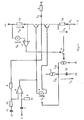
- 1 and 2 denote the two complementary output stage transistors, which are connected together with their emitters, to which the load impedance 3 is connected.
- the output stage transistors are biased by means of a bias voltage source 4.
- the input voltage is fed in the usual way via the connection 5 to a preamplifier 6 via a capacitor 7.
- the input of the preamplifier 6 is grounded via the resistor 8.
- the output of the preamplifier is connected to the bases of the output stage transistors 1 and 2.
- a negative feedback voltage passes from the output of the output stage via the resistor 9 to the inverting input of the preamplifier 6, which is grounded via the resistor 10 with the capacitor 11 connected in series with this.
- a resistor 12 is connected into the collector line of one transistor 1 of the output stage, at which a voltage U 1 arises as a result of the current flowing through it.
- the collector line of the other transistor 2 is also connected to a resistor 13 for the same purpose.
- the end of the resistor 13 connected to the collector of the transistor 2 is connected to the positive input of a voltage comparator 14, the negative input of which is supplied with a reference voltage Us.
- the voltage drop U 1 across the resistor 12 caused by the quiescent current IR of the output stage acts on a current source via the symbolically represented switch 15 16 a.
- the size of the voltage drop U1 ie the size of the current I 1 during the load phase of the final transistor 2, determines the discharge current of a capacitor 16, which is charged by a constant current source 17.
- the am Capacitor 16 standing voltage Depending on the size of the discharge current, ie depending on the resulting quiescent current of the output stage, the am Capacitor 16 standing voltage.
- the voltage influences or controls the bias voltage source 4 in such a way that the bias voltage UV becomes smaller as the quiescent current increases, as a result of which the quiescent current is regulated down.
- the principle of this regulation does not require any information about the voltage value at the load impedance 3. Only currents are evaluated.
- the load impedance 3 can therefore have any complex resistance, as is the case with loudspeakers, for example, without the quiescent current control being influenced in any way.
- the currents measured by resistors 12 and 13 can also be detected in other ways.
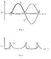
- FIG. 2 shows the different currents I 1 through the transistor 1, 1 2 through the transistor 2 and I L through the impedance 3.
- a quiescent current IR of the cross current IQ which flows through the transistors 1 and 2 in addition to the load current IL.
- FIG. 3 shows the course of the discharge current ICE together with the cross current IQ.
- the components provided with the same reference numerals in this figure correspond to those already described in FIG. 1.
- the output voltage of the preamplifier 6 here still reaches the output stage transistors 1 and 2 via driver transistors 18 and 19.
- the load resistances of the driver trans Sistors 18 and 19 are designated 20 and 21.
- the voltage U 1 is measured across the resistor 12 and is a measure of the cross current IQ during the active phase of the transistor 2. This voltage is evaluated as soon as the voltage drop across the resistor 13 caused by the load current IL is so great that it falls below the reference level Us.
- the reference level Us at the resistor 27 is generated by the constant current source with the resistor 23, the Zener diode 24 and the transistors 25 and 28 and the resistor 44.
- the components 22, 26 and 29 form a current mirror.
- the mirrored current through the transistor 29 becomes smaller than the current generated by the current mirror 28, 30, so that the transistor 32 comes out of saturation.
- the transistors 31, 37, 33, 43 and 34 form an operational amplifier, the non-inverting input of which is the base of the transistor 31 and the inverting input of which is the base of the transistor 37.
- This amplifier is fed back through the transistor 35, so that when the transistor 32 is not conductive, the voltage at the resistor 36 corresponds to the voltage U 1 at the resistor 12.
- the arrangement formed by transistors 31, 37, 33, 43, 34, 35 and resistor 36 is a voltage-current Converter.
- the transistor 35 controls depending on the measured
- Voltage U 1 is the discharge current ICE for the capacitor 16 charged by a quasi-constant current source 42.
- the voltage across the capacitor 16 acts on the bias voltage source 4 via the current mirror circuit formed by the transistors 38, the resistor 39 and the diode 40 and the transistor 41.
- increases the quiescent current the capacitor 16 is discharged, less current flows through the resistor 4 as a bias voltage source, so that the bias voltage decreases, which results in a reduction in the quiescent current in a desired manner. This closes the control loop.
- the circuit arrangement described can be applied to all series push-pull amplifiers whose quiescent current setting takes place via a DC voltage setting.
Landscapes
- Engineering & Computer Science (AREA)
- Power Engineering (AREA)
- Amplifiers (AREA)
Applications Claiming Priority (2)
| Application Number | Priority Date | Filing Date | Title |
|---|---|---|---|
| DE3343110 | 1983-11-29 | ||
| DE3343110A DE3343110C1 (de) | 1983-11-29 | 1983-11-29 | Transformatorlose Gegentaktendstufe |
Publications (3)
| Publication Number | Publication Date |
|---|---|
| EP0143375A2 true EP0143375A2 (fr) | 1985-06-05 |
| EP0143375A3 EP0143375A3 (en) | 1987-07-22 |
| EP0143375B1 EP0143375B1 (fr) | 1991-02-06 |
Family
ID=6215542
Family Applications (1)
| Application Number | Title | Priority Date | Filing Date |
|---|---|---|---|
| EP84113481A Expired - Lifetime EP0143375B1 (fr) | 1983-11-29 | 1984-11-08 | Amplificateur push-pull sans transformateur |
Country Status (4)
| Country | Link |
|---|---|
| EP (1) | EP0143375B1 (fr) |
| JP (1) | JPS60198907A (fr) |
| DE (2) | DE3343110C1 (fr) |
| HK (1) | HK10196A (fr) |
Cited By (5)
| Publication number | Priority date | Publication date | Assignee | Title |
|---|---|---|---|---|
| GB2217540A (en) * | 1988-04-12 | 1989-10-25 | Fluke Mfg Co John | Automatic biassing of amplifiers |
| EP0389654A1 (fr) * | 1989-03-29 | 1990-10-03 | Siemens Aktiengesellschaft | Circuit amplificateur intégré |
| GB2263034A (en) * | 1991-12-30 | 1993-07-07 | Harris Corp | Temperature compensation of amplifier in dependence on power handled |
| EP0540146A3 (fr) * | 1991-08-30 | 1994-03-09 | Nec Corp | |
| EP2114008A1 (fr) * | 2008-04-29 | 2009-11-04 | VLSI Solution Oy | Procédé pour commander un amplificateur et amplificateur |
Families Citing this family (3)
| Publication number | Priority date | Publication date | Assignee | Title |
|---|---|---|---|---|
| DE3632076A1 (de) * | 1986-05-23 | 1987-11-26 | Thomson Brandt Gmbh | Schaltungsanordnung zur automatischen einstellung des ruhestromes in einer gegentaktendstufe |
| DE3732915A1 (de) * | 1986-09-20 | 1989-04-13 | Thomson Brandt Gmbh | Schaltungsanordnung zur automatischen einstellung des ruhestroms in einer gegentaktendstufe |
| DE3744112A1 (de) * | 1987-12-01 | 1989-06-15 | Carl Spitzenberger | Verstaerkeranordnung |
Family Cites Families (10)
| Publication number | Priority date | Publication date | Assignee | Title |
|---|---|---|---|---|
| US3526845A (en) * | 1966-12-19 | 1970-09-01 | Nasa | Apparatus for overcurrent protection of a push-pull amplifier |
| US3536958A (en) * | 1967-12-05 | 1970-10-27 | Rca Corp | Amplifier protection circuit |
| US3553599A (en) * | 1968-02-20 | 1971-01-05 | Mitsubishi Electric Corp | Bias control circuit for semiconductor amplifier |
| US3731153A (en) * | 1970-08-27 | 1973-05-01 | Sansui Electric Co | Protective device for loudspeaker |
| DE2507741C3 (de) * | 1975-02-22 | 1979-05-17 | Deutsche Itt Industries Gmbh, 7800 Freiburg | Überstromgeschützte, universell verwendbare Transistoranordnung |
| US3974400A (en) * | 1975-09-05 | 1976-08-10 | Sony Corporation | Limiter circuit |
| DE2614399A1 (de) * | 1976-04-02 | 1977-10-06 | Rudolf Lender | Verfahren zur selbsttaetigen ruhestromeinstellung bei gegentaktsystemen |
| DE2725064C2 (de) * | 1977-06-03 | 1982-09-30 | Licentia Patent-Verwaltungs-Gmbh, 6000 Frankfurt | Komplementäre Gegentakt-Endstufe mit Kollektorstromregelung |
| DE2822037C2 (de) * | 1978-05-20 | 1980-07-24 | Braun Ag, 6000 Frankfurt | Schaltungsanordnung zur Regelung des Arbeitspunktes bei einem Gegentakt-B-Verstärker |
| US4237425A (en) * | 1979-05-03 | 1980-12-02 | Spiegel David A | Automatic bias adjusting circuit |
-
1983
- 1983-11-29 DE DE3343110A patent/DE3343110C1/de not_active Expired
-
1984
- 1984-11-08 EP EP84113481A patent/EP0143375B1/fr not_active Expired - Lifetime
- 1984-11-08 DE DE8484113481T patent/DE3484095D1/de not_active Expired - Fee Related
- 1984-11-29 JP JP59250677A patent/JPS60198907A/ja active Granted
-
1996
- 1996-01-18 HK HK10196A patent/HK10196A/xx not_active IP Right Cessation
Cited By (8)
| Publication number | Priority date | Publication date | Assignee | Title |
|---|---|---|---|---|
| GB2217540A (en) * | 1988-04-12 | 1989-10-25 | Fluke Mfg Co John | Automatic biassing of amplifiers |
| GB2217540B (en) * | 1988-04-12 | 1992-09-30 | Fluke Mfg Co John | Method and apparatus for automatically biasing a push-pull amplifier |
| US5034700A (en) * | 1989-03-19 | 1991-07-23 | Siemens Aktiengesellschaft | Integratable amplifier circuit |
| EP0389654A1 (fr) * | 1989-03-29 | 1990-10-03 | Siemens Aktiengesellschaft | Circuit amplificateur intégré |
| EP0540146A3 (fr) * | 1991-08-30 | 1994-03-09 | Nec Corp | |
| GB2263034A (en) * | 1991-12-30 | 1993-07-07 | Harris Corp | Temperature compensation of amplifier in dependence on power handled |
| GB2263034B (en) * | 1991-12-30 | 1996-05-01 | Harris Corp | Radio frequency amplifiers |
| EP2114008A1 (fr) * | 2008-04-29 | 2009-11-04 | VLSI Solution Oy | Procédé pour commander un amplificateur et amplificateur |
Also Published As
| Publication number | Publication date |
|---|---|
| EP0143375A3 (en) | 1987-07-22 |
| DE3343110C1 (de) | 1985-05-30 |
| EP0143375B1 (fr) | 1991-02-06 |
| JPS60198907A (ja) | 1985-10-08 |
| HK10196A (en) | 1996-01-26 |
| DE3484095D1 (de) | 1991-03-14 |
| JPH0580843B2 (fr) | 1993-11-10 |
Similar Documents
| Publication | Publication Date | Title |
|---|---|---|
| DE69026625T2 (de) | Stabilisierte gabelstromversorgung | |
| DE69423488T2 (de) | Spannungsregler | |
| DE69031277T2 (de) | Klangtreuer hörgerätverstärker | |
| DE2705201C3 (de) | Logarithmische Kompressionsschaltung | |
| DE2718491C2 (de) | Schaltungsanordnung zur Verstärkung der Signale eines elektromagnetischen Wandlers und zur Vorspannungserzeugung für den Wandler | |
| DE1907669C3 (de) | Temperaturkompensierte emittergekoppelte Schaltungsanordnung | |
| EP0143375B1 (fr) | Amplificateur push-pull sans transformateur | |
| DE3231829C2 (fr) | ||
| DE3011835C2 (de) | Leistungsverstärker | |
| DE3853425T2 (de) | Spannungsregelvorrichtung. | |
| DE3715238A1 (de) | Transistor-schalteinrichtung mit basisstrom-regulierung | |
| DE2328402A1 (de) | Konstantstromkreis | |
| DE2416533C3 (de) | Elektronische Schaltungsanordnung zur Spannungsstabilisierung | |
| DE69128652T2 (de) | Steuerschaltung | |
| EP0961403B1 (fr) | Circuit amplificateur intégré compensé en température | |
| DE2822037C2 (de) | Schaltungsanordnung zur Regelung des Arbeitspunktes bei einem Gegentakt-B-Verstärker | |
| DE3115051C2 (de) | Spannungs/Strom-Wandlerschaltung | |
| DE3931893A1 (de) | Schaltung zur strombegrenzung mit foldback-verhalten | |
| DE2911171C2 (de) | Schaltung für die Ansteuerung eines Stromquelletransistors | |
| DE2040531C3 (de) | Verfahren zum automatischen Einstellen der Ausgangsgleichspannung von Seriengegentaktverstärkern | |
| DE2359845C3 (de) | Schaltungsanordnung zur Konstanthaltung einer Gleichspannung | |
| DE3012823C2 (fr) | ||
| DE1613663B2 (de) | Schaltungsanordnung zur Konstanthaltung der Spannung an einem über Kabel angeschlossenen Verbraucher | |
| DE3742796C2 (fr) | ||
| DE2014610C3 (de) | Endstufenverstärker |
Legal Events
| Date | Code | Title | Description |
|---|---|---|---|
| PUAI | Public reference made under article 153(3) epc to a published international application that has entered the european phase |
Free format text: ORIGINAL CODE: 0009012 |
|
| AK | Designated contracting states |
Designated state(s): BE DE FR GB IT LU NL SE |
|
| PUAL | Search report despatched |
Free format text: ORIGINAL CODE: 0009013 |
|
| AK | Designated contracting states |
Kind code of ref document: A3 Designated state(s): BE DE FR GB IT LU NL SE |
|
| 17P | Request for examination filed |
Effective date: 19871221 |
|
| 17Q | First examination report despatched |
Effective date: 19891208 |
|
| GRAA | (expected) grant |
Free format text: ORIGINAL CODE: 0009210 |
|
| AK | Designated contracting states |
Kind code of ref document: B1 Designated state(s): BE DE FR GB IT LU NL SE |
|
| ITF | It: translation for a ep patent filed | ||
| REF | Corresponds to: |
Ref document number: 3484095 Country of ref document: DE Date of ref document: 19910314 |
|
| GBT | Gb: translation of ep patent filed (gb section 77(6)(a)/1977) | ||
| ET | Fr: translation filed | ||
| PLBE | No opposition filed within time limit |
Free format text: ORIGINAL CODE: 0009261 |
|
| STAA | Information on the status of an ep patent application or granted ep patent |
Free format text: STATUS: NO OPPOSITION FILED WITHIN TIME LIMIT |
|
| 26N | No opposition filed | ||
| EPTA | Lu: last paid annual fee | ||
| EAL | Se: european patent in force in sweden |
Ref document number: 84113481.0 |
|
| PGFP | Annual fee paid to national office [announced via postgrant information from national office to epo] |
Ref country code: SE Payment date: 19951122 Year of fee payment: 12 Ref country code: BE Payment date: 19951122 Year of fee payment: 12 |
|
| PGFP | Annual fee paid to national office [announced via postgrant information from national office to epo] |
Ref country code: NL Payment date: 19951130 Year of fee payment: 12 |
|
| PGFP | Annual fee paid to national office [announced via postgrant information from national office to epo] |
Ref country code: LU Payment date: 19960101 Year of fee payment: 12 |
|
| PG25 | Lapsed in a contracting state [announced via postgrant information from national office to epo] |
Ref country code: LU Free format text: LAPSE BECAUSE OF NON-PAYMENT OF DUE FEES Effective date: 19961108 |
|
| PG25 | Lapsed in a contracting state [announced via postgrant information from national office to epo] |
Ref country code: SE Effective date: 19961109 |
|
| PG25 | Lapsed in a contracting state [announced via postgrant information from national office to epo] |
Ref country code: BE Effective date: 19961130 |
|
| BERE | Be: lapsed |
Owner name: DEUTSCHE THOMSON-BRANDT G.M.B.H. Effective date: 19961130 |
|
| PG25 | Lapsed in a contracting state [announced via postgrant information from national office to epo] |
Ref country code: NL Effective date: 19970601 |
|
| NLV4 | Nl: lapsed or anulled due to non-payment of the annual fee |
Effective date: 19970601 |
|
| EUG | Se: european patent has lapsed |
Ref document number: 84113481.0 |
|
| REG | Reference to a national code |
Ref country code: GB Ref legal event code: 746 Effective date: 19970808 |
|
| PGFP | Annual fee paid to national office [announced via postgrant information from national office to epo] |
Ref country code: DE Payment date: 19991229 Year of fee payment: 17 |
|
| PGFP | Annual fee paid to national office [announced via postgrant information from national office to epo] |
Ref country code: GB Payment date: 20001009 Year of fee payment: 17 |
|
| PGFP | Annual fee paid to national office [announced via postgrant information from national office to epo] |
Ref country code: FR Payment date: 20001127 Year of fee payment: 17 |
|
| PG25 | Lapsed in a contracting state [announced via postgrant information from national office to epo] |
Ref country code: GB Free format text: LAPSE BECAUSE OF NON-PAYMENT OF DUE FEES Effective date: 20011108 |
|
| REG | Reference to a national code |
Ref country code: FR Ref legal event code: D6 |
|
| REG | Reference to a national code |
Ref country code: GB Ref legal event code: IF02 |
|
| GBPC | Gb: european patent ceased through non-payment of renewal fee |
Effective date: 20011108 |
|
| PG25 | Lapsed in a contracting state [announced via postgrant information from national office to epo] |
Ref country code: DE Free format text: LAPSE BECAUSE OF NON-PAYMENT OF DUE FEES Effective date: 20020702 |
|
| PG25 | Lapsed in a contracting state [announced via postgrant information from national office to epo] |
Ref country code: FR Free format text: LAPSE BECAUSE OF NON-PAYMENT OF DUE FEES Effective date: 20020730 |
|
| REG | Reference to a national code |
Ref country code: FR Ref legal event code: ST |
|
| REG | Reference to a national code |
Ref country code: FR Ref legal event code: ST |