EP0143533B1 - Expansions- und/oder Ziehungsverfahren und -gerät für Bilddaten - Google Patents
Expansions- und/oder Ziehungsverfahren und -gerät für Bilddaten Download PDFInfo
- Publication number
- EP0143533B1 EP0143533B1 EP84306633A EP84306633A EP0143533B1 EP 0143533 B1 EP0143533 B1 EP 0143533B1 EP 84306633 A EP84306633 A EP 84306633A EP 84306633 A EP84306633 A EP 84306633A EP 0143533 B1 EP0143533 B1 EP 0143533B1
- Authority
- EP
- European Patent Office
- Prior art keywords
- data
- matrix
- image data
- mapping pattern
- image
- Prior art date
- Legal status (The legal status is an assumption and is not a legal conclusion. Google has not performed a legal analysis and makes no representation as to the accuracy of the status listed.)
- Expired - Lifetime
Links
Images





















Classifications
-
- G—PHYSICS
- G06—COMPUTING OR CALCULATING; COUNTING
- G06T—IMAGE DATA PROCESSING OR GENERATION, IN GENERAL
- G06T3/00—Geometric image transformations in the plane of the image
- G06T3/40—Scaling of whole images or parts thereof, e.g. expanding or contracting
- G06T3/4023—Scaling of whole images or parts thereof, e.g. expanding or contracting based on decimating pixels or lines of pixels; based on inserting pixels or lines of pixels
Definitions
- the present invention relates to a method for expanding and/or contracting image information or data as well as an apparatus for carrying out the method.
- image data image information or data
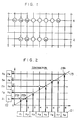
- image data X which include a string of n picture elements or pixels X1, X2, ..., X n arrayed one-dimensionally on latic points, as shown in Fig. 1, is to be contacted to image data Z including m pixels Z1, Z2, ..., Z m .
- the individual pixels X1, X2, ..., X n of the original image data are transformed to the indivudual pixels Z1, Z2, ..., Z5 of the output data 22 which are located on the left side to the corresponding lattice points 24a, 24b, ..., 24h. It will be seen that the pixels X1 and X2 are, respectively, transformed into the output pixel Z1, while the original pixels X6 and X7 are, respectively, transformed into the output pixel Z4.
- the output pixel Z1 is assumed to be constituted by the original pixel X1 with Z4 being constituted by X6.
- the expansion corresponds to the reversion of the contraction mentioned above.
- the expansion may be considered as the reversion of the contraction in which the original image data is replaced by the output data while the latter is replaced by the former.
- Fig. 3 illustrates a manner in which the original image data 25 of X1, ..., X5 are expanded to the output data 26 of Z1, Z2, ... Z8.
- the expansion or contraction of image data has been arithmetically determined for each of the pixels, as mentioned below.
- the expression for transformation of a pixel X i of the original image data 21 into a pixel Z j of the output data 22 is, by way of example, given by Z j ⁇ X i j ⁇ [ 5 8 i + 0.5] where [a] represents a maximum integer which does not exceed a .
- an object of the present invention is to eliminate the shortcomings of the prior art and provide a method and apparatus which are capable of performing image expansion and/or contraction at a significantly increased speed.
- an apparatus for expanding and contracting an image comprising a first register for storing original image data, a first barrel shifter for shifting said original image data, a register for storing a mapping pattern, an expansion and contraction circuit for expanding or contracting output data of said first barrel shifter under the control of said mapping pattern, a second barrel shifter for shifting output data of said expansion and contraction circuit, and a second register for storing output data of said second barrel shifter, wherein the register stores a mapping pattern which indicates positions of data to be extracted for the contraction of the image and indicates a number of times when the data is to be copied for the expansion of the image, whereby the image data stored in said storage means is expanded or contracted by referring to said mapping pattern, and wherein said register for storing the mapping pattern is implemented as a stack structure, and wherein in expanding or contracting a two-dimensional image, said mapping pattern is arithmetically determined in dependence on the ratio of expansion or contraction only once either in a vertical direction or in a horizontal direction or in both directions
- an apparatus for contracting an image comprising a matrix circuit (A) having n rows and n columns (where n is an integer greater than or equal to 2) data transmission means disposed at positions (a, k, l) of said matrix (A) (wherein k and l are integers), and data selecting means disposed at positions (a, m,q ) of said matrix (A) (where m and q are integers), wherein when the image data (x1, x2, ...
- x n ) to be contracted are moved from the n th row toward the first row, said data transmitting means disposed on the n th row sends out the image data (x) so that said image data (x) can be inputted to the data transmitting means or said data selecting means disposed on the (n-1) th row, while said data transmitting means disposed on the r th row (wherein r is an integer) sends out said image data (x) so that said image data (x) can be inputted to said data transmitting means or said data selecting means disposed on the (r-1) th row, and wherein said data selecting means disposed on the n th row determines whether the image data (x n ) to be contracted is to be discarded or not in dependence on a control signal which corresponds to a mapping pattern indicating portions of data to be extracted for the contraction of the image (P), and wherein said integers k and l are defined by x ⁇ k ⁇ n and k > l, said integers
- a mapping pattern indicating portions of data to be extracted for the contraction of an image and comprising at least binary data (P1, P2, ... P n ) which is applied to image data (x1, x2, ... x n ) to be contracted (where n is an integer greater than or equal to 2) is provided, and wherein said image data (x1, x2, ...
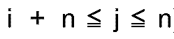
- x n ) to be contracted are moved within a matrix (A) including n rows and n columns from the n th row towards the first row, and when said mapping pattern P i (where i is an integer in the range of 1 ⁇ i ⁇ n) has a first value, the image data (x ) i located at a position (a ii ) of said matrix (A) are disclosed while the image data (x) located at a position (a ij ) (where i + n ⁇ j ⁇ n ) of said matrix (A) are moved to a position (a i-1,j-1 ) within said matrix (A), and when said mapping pattern (P i ) has a second value, the image data (x) located at a position (a i,j-1 ) of said matrix are moved to the position (a i-1,j-1 ) of said matrix (A), and wherein said mapping pattern is arithmetically determined in dependence on the ratio of contraction only once and is stored and then
- an apparatus for expanding an image comprising a matrix (A) of l rows and l' columns (where l and l ' are integers ⁇ 2), data transmitting means disposed at positions (a q,r ) (where q and r are integers given by 2 ⁇ q ⁇ l and q > r) of said matrix, data selecting means disposed at positions (a s,t ) (where s and t are integers given by 1 ⁇ s ⁇ l and s ⁇ t ⁇ l') and at the positions of the first row, wherein when the image data (x1, ..., x n ) to be expanded (where n is an integer ⁇ 1) are moved from the first row toward the l-th row, the data selecting means disposed on the first row responds to a control signal corresponding corresponding to a mapping pattern indicating a number of times the data is to be copied for the expansion of an image (P1) to input
- mapping pattern is a vector which includes components "0" and/or "1" and designates positions or locations of the elements of original image data which are to be extracted in the case of the contraction while indicating the number of times at which the individual elements are to be copied.
- mapping pattern P is represented as follows: A logical product of the above mapping pattern and the original image data X is determined for each of the elements to thereby obtain the output data Z by extracting the elements of the original image data X which correspond to "0" of the mapping pattern.
- the data to be processed is binary image data in which one bit corresponds to one picture element or pixel.
- a data bus is assumed to be 8 bits in width, and the processing is performed on the eight-bit basis. Further, input and output operations to and from each register are performed only on the eight-bit basis. (A set of eight bits may also be referred to as a word).
- Fig. 5 shows in a block diagram a general arrangement of the apparatus according to an exemplary embodiment of the invention.
- Original image data loaded in an input register 52 through a data bus 51 is shifted by a first barrel shifter 54 under the control of a control circuit 53.
- the output data of the shifter 54 is expanded or contracted by an expansion and contraction circuit 55 which is controlled in dependence on the mapping pattern.
- the output data of the expansion and contraction circuit 55 is, after having been shifted by a second barrel shifter 56, stored in an output register 57 to be available on the bus 51 for further processing.
- the input register 52 has a capacity of two words each of eight bits, wherein the eight more significant bits (MSB) and the eight less significant bits (LSB) can be inputted and outputted independent of each other. In this connection, it is assumed that the most significant bit is located at the leftmost position with the least significant bit being located at the rightmost position in the figures.
- the output register 57 has a capacity of two words and is so arranged that the more significant word and the less significant word can be inputted and/or outputted independently.
- the first barrel shifter 54 has an entrance of 16 bits in width and an exit of 8 bits, while the second barrel shifter 56 has an entry of 8 bits and an exit of 16 bits.
- the expansion and contraction circuit 55 is designed to perform the processing on the eight-bit basis.
- the mapping pattern 60 is arithmetically determined by a processing unit 60 and stored in a register 59 to be read out by a control register or mapping pattern register 58 on the eight-bit basis for controlling the expansion and contraction circuit 55.
- Fig. 6 shows an arrangement of the expansion and contraction circuit 55 according to an exemplary embodiment of the invention.
- the mapping pattern is read out from a register 61 on the eight-bit basis (i.e. eight-by-eight bits) and stored in a control register 62.
- the original image data of eight bits is stored in an input register 63.
- the registers 63 and 62 are constituted by shift registers which respond to clock signals a and d , respectively, for shifting the contents or data to the left, wherein the data appearing at the leftmost position of the register 63 is loaded in a buffer register 65.
- the clock signals a , b , c and d are of the same frequency and are delayed in phase by a small amount in the order of a , b , c and d .
- a numeral 67 denotes a switch circuit.
- the mapping pattern value e outputted from the control register 62 in response to the clock d is transmitted to a line f by way of the switch 67.
- the mapping pattern value e is transmitted to a line g .
- the leftmost one of the original image data in the register 63 is loaded in the buffer 65 in response to the clock a and then responds to the clock b to be written in a register 64 at an address h designated by an address counter 66.
- the address counter 66 performs a counting operation, whereby the mapping pattern placed in the control register 62 is shifted to the left in response to the clock d .
- the contracted data illustrated in Fig. 7A can be obtained in the output register 64 when eight cycles have elapsed from the starting time point.
- the original image data placed in the input register 63 is transferred to the buffer 65 in response to the clock a when the output value g of the mapping pattern is logic "l".
- the data in the buffer 65 in turn is written in the register 64 at the address h in response to the clock b .
- the address counter 66 operates in response to the clock c , which is followed by the shifting of the mapping pattern to the left in the register 62 in response to the clock d .
- the registers 62 and 63 are empty, while the register 64 is filled at the most significant five bits, as is illustrated in Fig. 7A.
- the register 62 is found in the empty state after the eight cycles, while the register 64 is fully filled and the register 63 contains three remaining bits, as is illustrated in Fig. 7B.
- mapping pattern and the original image data are supplied both on the eight-bit basis while the output data have to be read out every time the register 64 becomes full, requiring troublesome processing.
- This processing will be referred to as the register overflow processing.
- the mapping pattern is supplied on the eight-bit basis with the output data being read out also on the eight-bit basis.
- the loading of the original image data in the register 63 is required to be performed at the time point when the register 63 becomes empty, rendering the processing troublesome. (This processing will be referred to as the register empty processing).
- the memory for storing the original image data is usually so arranged that the reading of data can be performed on the 8-bit basis or on the 16-bit basis, it is impossible to read out the 8-bit data or 16-bit data from an arbitrarily selected position. It is common that the reading of data is permitted only from a predetermined position. (This position will be referred to as a word boundary.) In other words, the original image data as read out is always of eight bits from the word boundary.
- expansion or contraction processing which is so commanded as to start from a word boundary and come to an end at another word boundary is rather rare. In other words, in many practical cases, it is required that the expansion or contraction processing starts from an intermediate bit of a word and terminates at an intermediate bit of another word. This processing is naturally troublesome. (This processing will be referred to as the word boundary processing.)
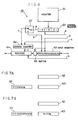
- the expansion and contraction circuit 55 is adapted to transform the original image data of eight bits into the left-aligned 5-bit output data at a contraction ratio of 5 8 in the contracting operation mode, as is illustrated in Fig. 8A.
- the expansion and contraction circuit 55 parforms translation of the left-aligned 5-bit original data into 8-bit output data at an expansion ratio of 8 5 , as illustrated in Fig. 8B.
- Fig. 9A shows, by way of example, a configuration of the first barrel shifter 54.
- a reference numeral 92 indicates cells each of which is constituted by a transfer gate of a structure schematically illustrated in Figs. 9B and 9C.
- the transfer gate is designed to interrupt the connection between signal lines p and q in response to control signal S.
- a given one of the control signals S1 to S8 is validated, a given set of eight bits can be selected from the two words of 16 bits contained in the original image data register 52.
- the control signal S6 is assumed to be validated or turned on.
- the data bit X'1 can not be straightforwardly transferred to a bit position of a register 91, this transfer of the bit X'1 to the register 91 can be accomplsihed by firstly reading out the least significant eight bits and writing them at the most significant eight bit positions, which is followed by the turning-on of the control signal S1, because the original image data register 52 is so arranged that the input/output of the most and less significant eight bits can be realized indepnendent of each other.
- the second barrel shifter 56 may, be of a configuration corresponding to the one shown in Fig. 9A except that the input and output sides are reversed or exchanged each other so that the 8-bit input can be transferred to given bit positions of the 16-bit output register 57.
- FIG. 10A the vertical lines 101 designates the boundary between words each of eight bits, and a hatched area 102 represents a single word consisting of eight bits or pixels (picture elements).
- the stored state is illustrated in Fig. 11.
- Step (2) From the mapping pattern register 59, the first eight bits of a mapping pattern are set at the control register 58, as illustrated in Fig. 12 at 123. The number C p of "1" present in the mapping pattern is set at a counter 128 (Fig. 12) which is also incorporated in the control circuit 53 shown in Fig.
- Step (6) No transfer takes place because the value C o of the output counter 126 is less than 8.
- Step (9) The step (2) mentioned above is regained and the processing is repeated to the step (5). These processing are illustrated at 131 to 134 in Fig. 12.
- Step (11) Since the value C o of the output counter 129 now exceeds the value "8", the most significant eight bits are transferred to the l-th word 111 of the output image data 110, while the least significant eight bits are shifted to the most significant bit positions.
- the (j+1)-th word is the last data of the first row.
- the processing described above in conjunction with the steps (2) to (5) is performed to thereby derive the contracted data illustrated at 144 in Fig. 12.
- the output data 145 are obtained through the processing of the step (10).
- l ⁇ l + 1 3.
- Step (15): The remaining pixel number n is renewed. Namely, n n - 8 0
- the steps (2) to (16) described above are repeatedly executed.
- the same mapping pattern as that for the first row can be used. Accordingly, it is convenient to construct the mapping pattern register 59, for example, in a stack configuration, whereby upon completion of the processing for one row, a stack pointer is returned to the initial or start position.
- the image expansion or contraction processing can be accomplished at a high speed because the individual steps can be executed on the eight-bit basis, without involving the register overflow processing or word boundary processing, by virtue of the combination of the expansion and contraction circuit 55 with a pair of 16-bit registers 52 and 57 and a pair of the barrel shifters 54 and 56 according to the teaching of the present invention.
- Step (2) The first eight bits of the mapping pattern is loaded from the mapping pattern register 59 in the control register 58, as illustrated at 153 in Fig. 14.
- Step (3): Eight pixels succeeding y3 inclusive thereof are extracted by the first barrel shifter 54. The number of shifting to be effected is given by the value C i ( 2) contained in the input counter 127.
- Step (6) The most significant eight bits of the output register 57 are transferred to the l-th word 104 of the output image data 103, while the less significant bits are shifted to the more significant bit positions.
- Step (11) Since the value of C i exceeds "8", the least significant eight bits in the input register 52 are shifted to the more significant bit positions, while the succeeding word 113 of the original image data is placed at the least significant eight bits position of the input register 52.
- Step (13) The five bits (C o ) of the output data 177 are aligned with the least significant three bits of the l -th word 107 of the output image data 103 and written in the word 107.
- Step (14) In dependence on the expansion or contraction ratio in the vertical direction, the row of the original image data to be subsequently processed is determined, and the processing at the steps (2) to (13) is repeated.
- the same mapping pattern as that used in the processing for the first row can be used in the processing of the second row.
- the expansion processing elucidated above can be executed at a high speed without requiring the register empty processing and the word boundary processing by virtue of the combination of the expansion and contraction circuit 55 with a pair of registers 52 and 57 and a pair of barrel shifters 54 and 56.
- the first barrel shifter has the entry of 16 bits in width and the exit of 8 bits in width.
- the entry and the exist of the first barrel shifter may be of more than 2n bits and n bits, respectively.
- width of the data bus is not restricted to eight bits.
- Fig. 16 shows schematically an arrangement of the contraction circuit according to another embodiment of the invention.
- a reference numeral 72 denotes a shift register for storing the original image data
- 76 denotes a shift register for storing output data
- a numeral 71 denotes a shift register for storing the mapping pattern.
- These shift registers 71, 76 and 72 are driven in response to the clock signals a , b and c which are delayed in phase relative to one another by a small amount in this order.
- the clock c applied to the register 72 causes the original image data stored therein to be shifted to the left, resulting in that the data bit located at the leftmost bit position (the most significant bit position) is transferred to a buffer 73.
- the data bit in the buffer 73 is loaded in the output shift register 76, provided that the pattern output d of the register 71 is logic or binary "1".
- the pattern output d is "0"
- the data in the buffer 73 is not written in the output register 76.
- Fig. 17 illustrates a circuit configuration for the expansion of image data. Only when the pattern output d of the mapping pattern register 71 is "1", the original image register 72 is shifted, whereby the data at the leftmost bit position is transferred to the buffer 73. On the other hand, when the pattern output d is "0", the shifting does not take place in the original data register 72, incurring no change in the content of the buffer 73.
- the clocks c , b and a are delayed in phase by a small amount in this order, as in the case of the contracting operation illustrated in Fig. 16.
- the same frequency may be employed as the clock signals for driving the registers 71, 72 and 76 shown in Figs. 16 and 17, involving no necessity for generating the frequency such as (m/n)f .
- the processing is effected in such a manner in which transformation (i.e. expansion or contraction) of one row is followed by the transformation of another row which is displaced from the one row in the vertical direction
- the mapping pattern P may be arithmetically determined and stored in a memory when the first row A of the original image is transformed into the first row B of the output image. Then, the transformation of the second row as well as the succeeding rows can be carried out by referring to the mapping pattern as stored. Accordingly, the processing speed can be increased ten or more times as high as the speed of processing in which the mapping pattern is determined for every transformation of the row.
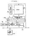
- the mapping pattern register of a stack configuration will be described by referring to Fig. 21.
- the image information or data is in general stored in a storage or memory device and processed by a computer, wherein arrangement is so made that the image data can be accessed on the 8-pixel basis or 16-pixel basis.
- the access to the mapping pattern should preferably be compatible with the access to the image data.
- the original image data of 16 bits are stored in the register 72 by way of a data bus 211 of 16 bits in width.
- the mapping pattern is arithmetically determined by a processing unit 213 on the 16-bit basis and stored sequentially in a first-in, first-out stack 214 of 16 bits in width.
- mapping pattern when the mapping pattern is required for the fifty bits, calculation of the mapping pattern is effected four times on the 16-bit basis, wherein the resulting four sets of mapping pattern data are sequentially stored in the stack 214.
- the address of the stored mapping pattern is designated by a stack pointer 215 and outputted to the mapping pattern register 71.
- the pattern output d of the register 71 is produced on a line e in the case of contraction through a switch 216 while the output d is transmitted to a line f in the case of expansion, thereby controlling the output register 76 in the former case or the original image data register 72 in the latter case.
- Step (1) A mapping pattern is calculated and stored in the stack 134.
- Step (2) Initial address is set at the stack pointer 215, whereby the mapping pattern located at the address designated by the stack pointer 215 is read into the mapping pattern register 71.
- mapping pattern is consumed in one cycle, whereby the output data of 16 bits is prepared by consuming a corresponding part of the original image data.
- mapping pattern and the original image data are updated or renewed at every cycle.
- the output data are read out when the output register is filled.
- mapping pattern is updated at every cycle with the output data being read out.
- the original image data are updated at a time point when it has been consumed.
- the stack pointer may be automatically incremented at every cycle.
- Step (5) When a two-dimensional image such as illustrated in Fig. 20 is to be processed, the mapping pattern for one row is divided into segments each of 16 bits and stored in the stack 134. Upon completion of the processing for one row, the stack pointer 135 is returned to the starting position. Thus, the succeeding rows inclusive of the second row can be processed in the similar manner.
- mapping patterns can be sequentially read out automatically merely by setting the stack pointer 215 at the time point when the processing for the first row is initiated, whereby the processing can be performed smoothly.
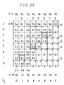
- the original image data X includes elements or bits x0, x1, x2, x3, x4, x5, x6 and x7 and that the mapping or mask pattern P for the reference consists of 1, 0, 1, 0, 0, 0, 1 and 0, as illustrated in Fig. 22.
- individual elements of the matrix illustrated in Fig. 22 is represented by M i,j where i designates rows and j designates columns.
- empty elements of the matrix may be set to "0".
- this circuit corresponds to the main portion of the circuit shown in Fig. 6 or the circuit shown in Fig. 16.
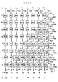
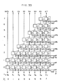
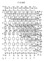
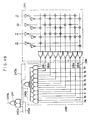
- Fig. 23 shows a wiring diagram of the data contracting circuit according to an exemplary embodiment of the invention.
- reference numerals 100 to 107 denote input terminals to which image data x0, ..., x7 to be contracted are applied
- 110 to 117 denote control input terminals to which a binary control signal corresponding to the reference mask pattern (mapping pattern) P0, ..., P7 is applied
- numerals 120 to 127 denote inverters, respectively.
- a reference numeral 13 denotes data transmitting means each provided at the location of element M j,k (where j and k are both integers and satisfy the conditions that 1 ⁇ j ⁇ 7 and that j > k) of a matrix consisting of eight rows and eight columns.
- the data transmitting means may simply be signal lines and serve for transmitting the data incoming from the above to the elements located below.
- a numeral 14 denotes data selecting means provided at locations of the matrix elements M s,t (where s and t are both integers and satisfy the conditions that 0 ⁇ s ⁇ 7 and s ⁇ t).
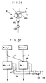
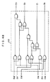
- the data selecting means may be constituted by logical elements 14a, 14b, 14c and 14d in a manner illustrated in Fig. 24 and serves for selecting one of data located at the matrix element M s+1, t+1 or the matrix element M s+1,t in dependence on the control signals a s and b s which correspond to the reference mask pattern (or mapping pattern) P s supplied through the control signal input terminals 11 s .
- the data selecting means 14 provided at the row 7 of the matrix shown in Fig. 23 serves only for determining whether the image data x7 is discarded or not.
- Reference numerals 150 to 157 denote output terminals through which the contracted data Y are obtained.
- the reference mask pattern (or mapping pattern) P consists of 1, 0, 1, 0, 0, 0, 1, 0 and the contracted data derived finally are represented by x0, x2, x6, as described hereinbefore in conjunction with Fig. 22.
- the original image data bits x0, ..., x5 located at the data transmitting means 130, 131, ..., 135 are sent to the data transmitting means 137, 138, ..., 1312.
- the original image data x0, x1, ..., x4 present at the data transmitting means 137, 138, ..., 1311 are sent out to the data transmitting means 1313, 1314, ..., 1317.
- the original image data x0, x1, ..., x3 present on the data transmitting means 1313, 1314, ..., 1316 are sent out to the data transmitting means 1317, 1318, ..., 1320.
- the original image data x0, x1, x2 present at the data transmitting means 1317, 1318, 1319 are sent out to the data transmitting means 1321, 1322, 1323.
- the original image data x0 and x1 present at the data transmitting means 1321 and 1322 are sent out to the data transmitting means 1324 and 1325, respectively.
- the original image data bit x0 of the data transmitting means 1324 are sent out to the data transmitting means 1326.
- the contracted data Y can be obtained.
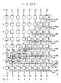
- the matrix-like array of the data transmitting means 13 and the data selecting means 14 data contraction can be carried out at a high speed without requiring the clocking. Further, due to the regular circuit configuration, the matrix circuit is suited to be implemented in the form of LSI (large scale integrated circuit). Besides, merely by varying the control signal applied to the control signal input terminal 11, contracted data Y of the other types can be produced easily.
- LSI large scale integrated circuit
- the data transmitting means is assumed to be provided in the embodiment described above, this is only for convenience of illustration. Since the data transmitting means 13 may be replaced by simple signal lines, as noted earlier, the circuit shown in Fig. 24 may be modified to a configuration shown in Fig. 27.
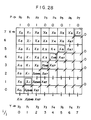
- the original image data X include elements or bits x0, x1, x3, x4, x5, x6, x7 and that the reference mask pattern P consists of 1, 0, 1, 0, 0, 0, 1, 0, as is illustrated in Fig. 28.
- individual elements of the matrix illustrated in Fig. 28 are represented by M i,j where i designates rows and j designates columns.
- the reference mask pattern P i is "1”
- all the elements present at that time on the row i are moved to the row (i - 1).
- the method described here differs from the one described with reference to Fig. 22 in that the logical sum is got.
- empty elements of the matrix may be set to "0".
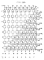
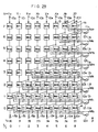
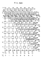
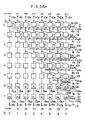
- Fig. 29 shows a wiring diagram of the data contracting circuit according to an exemplary embodiment of the invention.
- reference numerals 100 to 107 denote input terminals to which image data x0, ..., x7 to be contracted are applied
- 110 to 117 denote control input terminals to which binary control signals corresponding to the reference mask pattern (mapping pattern) P0, ..., P7 are applied
- numerals 120 to 127 denote inverters, respectively.
- a reference numeral 13 denotes data transmitting means each provided at the location of element M j,k (where j and k are both integers and satisfy the conditions that 1 ⁇ j ⁇ 7 and j > k + 1) of a matrix consisting of eight rows and eight columns.
- the data transmitting means may simply be signal lines and serve for transmitting the data incoming from the above to the elements located below.
- a numeral 14 denotes data selecting means provided at locations of the matrix elements M s,t (where s and t are both integers and satisfy the conditions that 0 ⁇ s ⁇ 7 and s ⁇ t.).
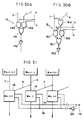
- the data selecting means may be constituted by logical elements 14a, 14b, 14c and 14d in a manner illustrated in Fig. 30 and serves for selecting one of data located at the matrix element M s+1,t+1 or the matrix element M s+1,t in dependence on the control signals a s and b s which correspond to the reference mask pattern P5 supplied through the control signal input terminals 115. It should however be noted that the data selecting means 14 provided at the row 7 of the matrix M serves only for determining whether the image data is to be discarded or not.
- a reference numeral 16 denotes data selecting means located at the position of the matrix element M i,i-1 and serving for selecting either one of the logical sum of the data located at the matrix elements M i+1,i and M i+1,i-1 or the data located at the matrix element M i+1,i-1 in dependence on the control signals a i and b i which correspond to the reference mask pattern P i supplied through the control input terminal 11 i .
- This data selecting means 16 is composed of logical elements 16a, 16b, 16c, 16d and 16e connected in the manner illustrated in Fig. 30.
- the data selecting means 16 differs from the data selecting means 14 in that a logical sum of data d and c is inputted in place of the data c .
- Refrence numerals 150 to 157 denote output terminals through which the contracted data Y are obtained.
- the reference mask pattern P consists of 1, 0, 1, 0, 0, 0, 1, 0 and the contracted data derived finally are represented by x0 + x1, x2 + x3 + x4 + x5, x6 + x7, as described hereinbefore in conjunction with Fig. 28.
- the original image data bits x0, ..., x4 located at the data transmitting means 130, 131, ..., 134 are sent to the data transmitting means 136, 137, ..., 1310.
- the original image data x0, x1, x2, x3 present at the data transmitting means 136, 137, 138, 139 are sent out to the data transmitting means 1311, 1312, 1313, 1314.
- the original image data x0, x1, x2 present on the data transmitting means 1311, 1312, 1313 are sent out to the data transmitting means 1315, 1316, 1317.
- the original image data information x0, x1 present at the data transmitting means 1315 and 1316 are sent out to the data transmitting means 1318 and 1319.
- the data on the line C is selected by the data selecting means 144, allowing the original image data bit x6 to be inputted, while the data selecting means 164 selects the logical sum x2345 of the signals on the lines E and F.
- the original image data x0 present at the data transmitting means 1318 are sent out to the data transmitting means 1320.
- the contracted data Y can be obtained.
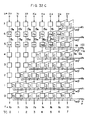
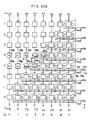
- the matrix-like array of the data transmitting means 13 and the data selecting means 14 and 16 data contraction can be carried out at a high speed without requiring clocking. Further, due to the regular circuit configuration, the matrix circuit is suited to be implemented in the form of LSI. Further, by deriving the logical sum of the adjacent data upon contraction of the original image data, the logic "l" data will not disappear. Accordingly, the frame of table prepared by the logic "l" bits is not erased by the data contraction. Besides, merely by varying the control signal applied to the control signal input terminal 11, the contracted data Y of the other type can be produced easily.
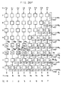
- the data transmitting means are assumed to be provided in the embodiment described above, this is only for convenience of illustration. Since the data transmitting means 13 may be replaced by simple signal lines, as described earlier, the circuit shown in Fig. 29 may be modified to a configuration shown in Fig. 33.
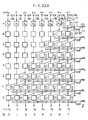
- the original image data X includes elements or bits x0, x1, x2, x3, x4, x5, x6 and x7 and that the mapping or reference mask pattern P consists of 1, 0, 1, 0, 0, 0, 1, 0 as illustrated in Fig. 34.
- Fig. 34 individual elements of the matrix illustrated in Fig. 34 are represented by M i,j where i designates rows and j designates columns.
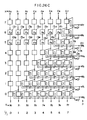
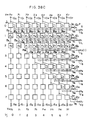
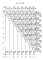
- Fig. 35 shows a wiring diagram of the data expanding circuit according to an exemplary embodiment of the invention.
- reference numerals 100 to 107 denote input terminals to which image data x0, ..., x7 to be expanded are applied
- 110 to 117 denote control input terminals to which a binary control signal corresponding to the reference mask pattern (mapping pattern) P0, ..., P7 is applied
- numerals 120 to 127 denote inverters, respectively.
- a reference numeral 13 denotes data transmitting means each provided at the location of element M j,k (where j and k are both integers and satisfy the conditions that 1 ⁇ j ⁇ 7 and j > k) of a matrix consisting of eight rows and eight columns.
- the data transmitting means may simply be signal lines and serve for transmitting the data incoming from the above to the elements located below.
- a numeral 14 denotes data selecting means provided at locations of the matrix elements M s,t (where s and t are both integers and satisfy the conditions that 0 ⁇ s ⁇ 7 and s ⁇ t).
- the data selecting means may be constituted by logical elements 14a, 14b, 14c and 14d in the manner illustrated in Fig. 36 and serves for selecting one of data located at the matrix element M s-1,t-1 or the matrix element M s-1,t in dependence on the control signals a s and b s which correspond to the reference mask pattern (or mapping pattern) P s supplied through the control signal input terminals 11 s .
- Reference numerals 150 to 157 denote output terminals through which the expanded image Y are obtained.
- the reference mask pattern (or mapping pattern) P consists of 1, 0, 1, 0, 0, 0, 1, 0 and the expanded data to be derived finally is represented by x0, x0, x1, x1, x1, x1, x2, x2.
- the original image data bits x0 located at the data selecting means 140 is sent to the data transmitting means 130.
- the original image data x0 present at the data transmitting means 130 and the data selecting means 148 are sent out to the data transmitting means 131 and 132.
- the original image data x0 and x1 present on the data transmitting means 131 and 132 and the data selecting means 1415, respectively, are sent out to the data transmitting means 133, ..., 135.
- the original image data x0 and x1 present at the data transmitting means 133, 134, 135 and the data selecting means 1421 are sent out to the data transmitting means 136, ..., 139.
- the data on the lines C12, ..., C15 are selected, allowing the original image data x1, ..., x4 to be inputted.
- the original image data x0 and x1 present at the data transmitting means 136, ..., 139 and the data selecting means 1426, respectively, are sent out to the data transmitting means 1310, ..., 1314, respectively.
- the original image data bit x0 and x1 of the data transmitting means 1310, ..., 1314 and the data selecting means 1430, respectively, are sent out to the data transmitting means 1315, ..., 1320.
- the image data x0, x1, x2 at the signal transmitting means 135, ..., 1316 and the data selecting means 1433 are sent out to the signal transmitting means 1321, ..., 1327, respectively.
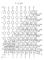
- the matrix-like array of the data transmitting means 13 and the data selecting means 14 data expansion can be carried out at a high speed without requiring clocking. Further, due to the regular circuit configuration, the matrix circuit is suited to be implemented in the form of LSI. Besides, merely by varying the control signal applied to the control signal input terminal 11, the expanded data Y of the other type can be produced easily.
- the data transmitting means 13 are assumed to be provided in the embodiment described above, this is only for convenience of illustration. Since the data transmitting means 13 may be replaced by simple signal lines, as described earlier, the circuit shown in Fig. 35 may be modified to a configuration shown in Fig. 39.
- the circuit shown in Fig. 29 is so arranged that the data at the mapping pattern "1" is logically ORed with the data at the succeeding mapping pattern so that the final data x 0,1 , x 2,3,4,5 , x 6,7 may be obtained.
- the notation x i,j,k represents the logical sum of the data x i , x j and x k .
- the wiring from a given element M i,i on the diametrical line to an adjacent element M i,i-1 located on the left side of the given element M i,i in the contraction circuit shown in Fig. 23 is changed as shown in Fig. 29.
- the data at M i+1,i-1 are stored as they are.
- the data at M i+1,i-1 is ORed with the data at M i+1,i in the processing at the mapping pattern "0".
- the logical sum for the first data is not got.
- auxiliary register 580 which may be used in the expansion or contraction circuit according to the invention.
- the number of data processed in a single processing corresponds to the number of "1" present in the mapping pattern in the case of the expansion processing, while the number of data processed is always equal to 8 in the case of the contraction processing, as will be seen from Figs. 2 and 3.
- the number of data produced through a single processing is constantly eight in the case of the expansion processing, while the number of data in question corresponds to the number of "1" present in the mapping pattern in the case of contraction.
- the original image data stored in the input register 52 is shifted upon every processing to the left by a number corresponding to the number of bits "1" included in the mapping pattern (the number of bits "1" included in the mapping pattern will be hereinafter represented by NB), wherein the resulting empty bit positions are filled with the bits of the succeeding original image data.
- NB the number of bits “1” included in the mapping pattern
- data is renewed at the bit "1" of the mapping pattern, while the preceding data are copied at the bit "0" of the mapping pattern. Accordingly, when the leading data bit of the mapping pattern is "0", as illustrated in Fig. 40 by a reference numeral 1910, the final data x5 which has been produced through the immediately preceding processing becomes necessary.
- the auxiliary register 580 for storing the required data bit in the data produced through the immediately preceding processing is provided on the left side to the input register 52, as is shown in Fig. 40. Since the data x5 is the final pixel data FB generated through the preceding processing, the data FB is extracted with the aid of an arithmetic circuit 590 and loaded in the auxiliary register 580.
- the arithmetic circuit or unit 590 serves to arithmetically determine the data to be supplied to the auxiliary data register 580 in the expansion or contraction processing. Details of this arithmetic circuit will be described later or by referring to Figs. 45 to 50. In contrast, when the leading bit of the mapping pattern is "1", as indicated in Fig. 40 by a reference numeral 1920, there arises no necessity for returning the final data bit FB to the auxiliary register 580.
- the original image data stored in the input register 52 are all referred to and utilized on the eight-bit basis upon every processing inclusive of the processing in which a logical sum is got. Accordingly, the original image data in the register 52 are all replaced by the fresh data upon every processing.
- the logical sum is to be determined in the contraction processing, the data corresponding to the bit "1" of the mapping pattern is ORed with the data corresponding to the bit "0" of the mapping pattern. Accordingly, when the leading bit of the mapping pattern is "0", as indicated by a reference numeral 2010, the final data bit FB contained in the data prepared through the preceding processing is required for realizing the logical OR-function.
- the final bit FB is extracted by means of the arithmetic circuit 590 and stored in the auxiliary register 580.
- the number of data bits to be produced corresponds to NB (which represents the number of "1" included in the mapping pattern) plus 1(one).
- NB is 4 and 2, respectively, while the number of the produced data is 5 and 3, respectively.
- x78 should be replaced by x781'.
- the arithmetic circuit 590 plays no part when the leading bit of the mapping pattern is "1". In this case, data in the auxiliary register is indeterminate or indefinite. When the leading bit of the mapping pattern is "0" in the expansion processing, the eighth pixel data of those generated through the preceding processing is returned to the auxiliary register 580.
- the counting of the number of "1" contained in the mapping pattern may be realized, for example, by shifting the mapping pattern bit by bit and counting the number of times when the carry is set.
- the left input to the top left element M00 shown in Fig. 35 is connected to the ground. This left input is disconnected from the ground and connected to the auxiliary register 580 as indicated by an input line 2110 to the element M00 in Fig. 42.
- a circuit similar to the bottom left element M00 shown in Fig. 23 is additionally provided on the left side of the latter and connected to the output x M of the auxiliary register 580, as is shown in Fig. 43 (where A represent a circuit point to which the logic "l" signal is applied). Then, the leading data x781' generated through the second processing shown in Fig. 41 appears at the output y M which is positioned on the left side to the output y0. Accordingly, one bit position is additionally provided in the output register at the left, to store the output y M . The processing of the generated data may be effected including this data y M .
- the number of data produced through the first processing was not five but in fact four. This fact can be indicated only by the leading bit of the mapping pattern for the second processing, thus involving a difficulty in the execution of the processing.
- an output auxiliary register 2110 is provided on the left side to the output register 57 as shown in Fig. 44, wherein the data produced in correspondence to the leading bit of "1" of the mapping pattern are stored in the output auxiliary register 2110 for replacing the final data produced through the preceding processing by the data stored in the register 2110. More specifically, taking as an example the second processing illustrated in Fig. 44, the data x78 in the auxiliary register 580 is ORed with x1', resulting in x781' which is then stored in the output auxiliary register 2110, whereby the final data x78 produced through the first processing is replaced by x781'.
- the fourth data x 7'8' is returned to the auxiliary register 580.
- the leading data of the mapping pattern is "1”
- the number of data as generated is equal to NB.
- the NB-the data bit is returned to the auxiliary register 580.
- the data to be stored in the auxiliary register 580 is produced through the preceding processing. Accordingly, a storage means for storing this data is required to be provided independent of the input register.
- a selector 241 is controlled by control signals 242a or 242b which are changed over in dependence on the expansion processing or contraction-OR processing (i.e. contraction processing including the logical OR function), to select the eight data bit 243a of the data 51a generated by the expansion and contraction circuit 55 in the case of the expansion processing.
- the selector 241 responds to a decoded signal 247a outputted from a decoder 246 which is supplied with a singal 245a produced by a binary data counting circuit 244 and representing NB which is the number of bits "1" included in the mapping pattern stored in the control register 58, to thereby select the NB-the data bit 243b of the generated data 51a.
- Figs. 46, 47 and 48 show an exemplary embodiment of the binary data counting circuit 244.
- Fig. 46 shows the same in a block diagram.
- the mapping pattern consisting of 8 bits is divided into two segments each of 4 bits.
- a pair of one-bit adders 1011 and 1012 provided at the first stage determine the number of "1" included in the respective inputs each of 3 bits (i.e. a7, a6, a5 for the adder 1011, and a3, a2, a1 for the adder 1012), which is followed by the determination of the number of "1" included in 4 bits by incrementers 1021 and 1022, respectively.
- a three-bit adder 110 determines the number of "1" included in the mapping pattern of 8 bits, this number being outputted as the four-bit signal 245a.
- a circuit configuration of the one-bit adder 1012 and the incrementer 1022 for the four bits a3, a2, a1, a0 is shown in Fig. 47.
- Two bits a3 and a2 of the 4-bit input data A(a3, a2, a1, a0) denoted by a numeral 71 are added by means of an adder constituted by an AND (logical product) circuit 921 and an EOR (Exclusive-OR) circuit 922, whereby a sum signal ⁇ 00 and a carry C00 are produced.
- the sum signal ⁇ 00 and the bit a1 of the input data 71 are added by an adder constituted by an AND circuit 931 and an EOR circuit 932, resulting in that a sum signal ⁇ 10 and a carry signal C10 are produced.
- the signals C00 and C10 are combined by a NAND circuit 96 to produce a carry signal C20.
- the number of "1" included in three bits a3, a2, a1 of the input data 71 is represented by the sum ⁇ 10 and the carry C20.
- the sum signal ⁇ 10 and the bit a0 of the input data 71 are added by an adder constituted by an AND circuit 971 and an EOR circuit 972, whereby a sum signal ⁇ 30 and a carry signal C30 are produced.
- the carry signals C30 and C20 are added by an adder constituted by an AND circuit 981 and an EOR circuit 982, resulting in that sum signals ⁇ 31 and ⁇ 32 are produced.
- Fig. 49 shows a circuit diagram of the decoder 246 and the selector 241.
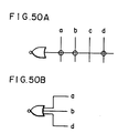
- the meaning of symbols used in the decoder 246 is illustrated in Fig. 50. More specifically, a circuit configuration shown in 50A is equivalent to that shown in Fig. 50B.
- ⁇ 3, ⁇ 2, ⁇ 1 and ⁇ 0 represent the number NB of "1" contained in the mapping pattern.
- a signal 281a is logic "l"
- y M is outputted as the signal 243b.
- y0, y1, ..., or y7 is correspondingly outputted as the signal 243b.
- the signal 242b is logic "l", while the signal 242a is “0”, whereby the signal 243b is outputted on the line 249a to be subsequently stored in the auxiliary register 580.
- the signal 242b is "0” and 242a is "1”, whereby y7 is constantly outputted on the line 249a to be stored in the auxiliary register.
Landscapes
- Physics & Mathematics (AREA)
- General Physics & Mathematics (AREA)
- Engineering & Computer Science (AREA)
- Theoretical Computer Science (AREA)
- Image Processing (AREA)
Claims (12)
- Vorrichtung zum Expandieren und Kontrahieren eines Bildes, mit einem ersten Register (52) zum Speichern von Orginalbilddaten, einem ersten Mengenumsetzter (54) zum Umsetzen der Orginalbilddaten, einem Register (58, 59; 61, 62; 71, 214, 215) zum Speichern eines Abbildemusters, einer Expansions- und Kontraktionsschaltung (55) zum Expandieren oder Kontrahieren von Ausgangsdaten des ersten Mengenumsetzers (54) unter der Steuerung des Abbildemusters, einem zweiten Mengenumsetzer (56) zum Umsetzen von Ausgangsdaten der Expansions- und Kontraktionschaltung (55) und einem zweiten Register (57) zum Speichern von Ausgangsdaten des zweiten Mengenumsetzers (56), wobei das Register (59; 71) ein Abbildemuster (P) speichert, das Positionen von zu extrahierenden Daten für die Kontraktion des Bildes anzeigt und eine Anzahl von Zeiten anzeigt, zu denen die Daten für die Expansion des Bildes zu kopieren sind, wodurch die in der Speichereinrichtung (52) gespeicherten Bilddaten unter Einbeziehung des Abbildemusters expandiert oder kontrahiert werden, und wobei das Register (71) zum Speichern des Abbildemusters als eine Stapelstruktur (71, 214, 215, Fig. 21) implementiert ist, und wobei beim Expandieren oder Kontrahieren eines zweidimensionalen Bildes das Abbildemuster arithmetisch in Abhängigkeit vom Expansions- oder Kontraktionsverhältnis nur einmal bestimmt wird, und zwar in einer vertikalen Richtung oder in einer horizontalen Richtung oder in beiden Richtungen, wobei die Expansion oder Kontraktion unter Einbeziehung des Abbildemusters erfolgt.
- Vorrichtung zum Expandieren und Kontrahieren eines Bildes nach Anspruch 1, bei der dann, wenn ein Expansionsverhältnis mit n/m gegeben ist und ein Kontraktionsverhältnis mit m/n gegeben ist (wobei n > m), sowohl das erste als auch das zweite Register (52, 57) 2n Bits haben, das erste Mengenregister einen Eingang von 2n Bits und einen Ausgang von n Bits hat, während das zweite Mengenregister einen Eingang von n Bits und einen Ausgang von 2n Bits hat.
- Bildexpansions- und Kontraktionsvorrichtung nach Anspruch 2, mit einem zweiten Register (580) zum Speichern der letzten Bildpunktdaten einer durch die Expansions- oder Kontraktionsverarbeitung erzeugten Bildpunktdatenkette, wobei die Expansions- und Kontraktionsschaltung (55) dazu dient, das Bild dadurch zu expandieren oder kontrahieren, daß gleichzeitig mehrere in der Speichereinrichtung und dem zweiten Register gespeicherte Bilddaten unter Einbeziehung des Abbildemusters verarbeitet werden.
- Bildexpansions- und Kontraktionsvorrichtung nach Anspruch 3, mit einer logischen Arithmetikschaltung (244, 246, 248, 241) zum Extrahieren der letzten Bildpunktdaten der durch die Expansions- oder Kontraktionsverarbeitung erzeugten Bildpunktdatenkette.
- Vorrichtung zum Kontrahieren eines Bildes mit einer Matrixschaltung (A) mit n Reihen und n Spalten (wobei n eine ganze Zahl größer oder gleich 2 ist), einer Datenübertragungseinrichtung an Positonen (a k,l) der Matrix (A) (wobei k und l ganze Zahlen sind) und einer Datenwähleinrichtung an Positionen (am,q) der Matrix (A) (wobei m und q ganze Zahlen sind), wobei dann, wenn zu kontrahierende Bilddaten (x₁,x₂,...xn) von der n - ten Reihe zur ersten Reihe verbracht werden sollen, die Datenübertragungseinrichtung an der n-ten Reihe die Bilddaten (x) aussendet, so daß die Bilddaten (x) der Datenübertragunseinrichtung (13) oder der Datenwähleinrichtung an der (n-1)-ten Reihe eingegeben werden könen, während die Datenübertragunsgeinrichtung an der r-ten Reihe (wobei r eine ganze Zahl ist) die Bilddaten (x) aussendet, so daß die Bilddaten (x) der Datenübertragungseinrichtung (13) oder der Datenwähleinrichtung an der (r-1)-ten Reihe eingegeben werden können, und wobei die Datenwähleinrichtung an der n-ten Reihe feststellt, ob die zu kontrahierenden Bilddaten (xn) fallengelassen werden sollen oder nicht, und zwar abhängig von einem Steuersignal, das einem Abschnitte von für die Kontraktion des Bildes (P) zu extrahierenden Daten anzeigenden Abbildemuster entspricht, und wobei die ganzen Zahlen k und l durch x ≦ k ≦ n und k > l bestimmt sind, die ganzen Zahlen m und q durch 1 ≦ m < n und q > m bestimmt sind, die ganze Zahl r in dem Bereich

- Vorrichtung zum Kontrahieren eines Bildes nach Anspruch 5, bei der die ganzen Zahlen k und l durch 3 ≦ k < n und k > l+1 bestimmt sind, die ganzen Zahlen m und q durch 1 ≦ m < n und q ≧ m -1 bestimmt sind, die ganze Zahl r in dem Bereich

- Vorrichtung zum Kontrahieren eines Bildes nach Anspruch 5 oder 6, bei der die Datenübertragungseinrichtung aus Verdrahtungsleitungen zusammengesetzt ist.
- Verfahren zum Kontrahieren von Bilddaten, bei dem ein Abbildemuster vorgesehen ist, das für die Kontraktion eines Bildes zu extrahierende Datenabschnitte anzeigt und mindestens auf die zu kontrahierenden Bilddaten (x₁, x₂,..... xn) anzuwendende binäre Daten (P₁,P₂, ...Pm) aufweist (wobei n eine ganze Zahl größer oder gleich 2 ist), und bei dem die zu kontrahierenden Bilddaten (x₁,x₂, .... xn) innerhalb einer n Reihen und n Spalten beinhaltenden Matrix (A) von der n-ten Reihe gegen die erste Reihe bewegt werden, und dann, wenn das Abbildungsmuster Pi (wobei i eine ganze Zahl im Bereich von 1 ≦ i ≦ n ist) einen ersten Wert hat, die Bilddaten (x) an einer Position (aii) der Matrix (A) freigegeben werden, während die Bilddaten (x) an einer Position (aij) (wobei
- Verfahren zum Kontrahieren von Bilddaten nach Anspruch 8, bei dem eine logische Operation an den Bilddaten (xi) an einer Position (aii) der Matrix (A) dann ausgeführt wird, wenn das Abbildemuster (Pi) (wobei i eine ganze Zahl in dem Bereich von 1 ≦ i ≦ n ist) einen ersten Wert hat, wobei das Ergebnis der logischen arithmetischen Operation an eine Postion (ai-1,i-1) bewegt wird, während Bilddaten (x) an einer Position (aij) (wobei j eine ganze Zahl in dem Bereich von


- Verfahren zum Expandieren eines Bildes, bei dem ein Abbildemuster vorgesehen ist, das eine Anzahl von Malen, die die Daten für die Expansion eines Bildes zu kopieren sind, anzeigt und mindestens auf die zu expandierenden Bilddaten (x₁,x₂,...,xn) (wobei n eine ganze Zahl ≧ 1 ist) anzuwendende binäre Daten (Pm) aufweist (wobei m eine ganze Zahl ≧ 1 ist), und bei dem, während die zu expandierenden Bilddaten (x₁, x₂,...,xn) innerhalb einer Matrix (A) mit l Reihen und l' Spalten (wobei l und 1' ganze Zahlen ≧ 2 sind) in der Richtung von der ersten Reihe auf die l-te Reihe bewegt werden, wenn das Abbildemuster (Pi) einen ersten Wert hat (wobei i eine ganze Zahl in dem Bereich von 1 ≦ i ≦ l ist), die Bilddaten (x) an einer Position (ai,j) (wobei j eine Zahl in dem Bereich von i ≦ j ≦ l ist) an eine Position (ai+1,j+1) der Matrix und die Bilddaten (x) an einer Position (ai,k) (wobei k eine ganze Zahl kleiner als i und nur 1 ist, wenn i = 1) an eine Position (ai+1,k) bewegt werden, und dann, wenn das Abbildemuster (Pi) einen zweiten Wert hat, die Bilddaten (x) an einer Position (ai,p) (wobei p eine ganze Zahl in den Bereich von 1 ≦ p ≦ l ist) der Matrix (A) an eine Position (ai+1,p) der Matrix (A) bewegt werden, wobei das Abbildemuster arithmetisch in Abhängigkeit vom Expansionsverhältnis nur einmal bestimmt und gespeichert wird und dann für nachfolgende Übertragungen ohne die Notwendigkeit erneuter Berechnungen verwendet wird.
- Vorrichtung zum Expandieren eines Bildes, mit einer Matrix (A) von l Reihen und l' Spalten (wobei l und l' ganze Zahlen ≧ 2 sind), einer Datenübertragungseinrichtung (13) an Positionen (aq,r) (wobei q und r ganze Zahlen entsprechend den Ungleichungen 2 ≦ q < l und q > r sind) der Matrix, einer Datenwähleinrichtung (14) an Positionen (as,t) (wobei s und t ganze Zahlen entsprechend den Ungleichungen 1 < s ≦ l und s ≦ t ≦ l' sind) und an den Positionen der ersten Reihe, wobei dann, wenn die zu expandierenden Bild- daten (x₁,...,xn) (wobei n eine ganze Zahl ≧ 1 ist) von der ersten Reihe gegen die l-te Reihe bewegt werden, die Datenwähleinrichtung (14) an der ersten Reihe, ansprechend auf ein dem Abbildemuster, das eine Anzahl von Malen anzeigt, die die Daten für die Expansion eines Bildes (P₁) zu kopieren sind, entsprechendes Steuersignal, eines der zu expandierenden Bilddaten (xu,xu+1) (wobei 1 ≦ u < n und u = 1 nur für u + 1 = 1) eingibt, während die Datenwähleinrichtung (14) an der Position (as,t) der Matrix, ansprechend auf das dem Abbildemuster (Ps) entsprechende Steuersignal, die Bilddaten (x) von der Datenwähleinrichtung eingibt, die entweder an der Position (as-1,t-1) oder an der Position (as-1,t) angeordnet ist, und die Datenübertragungseinrichtung an der Position (aq,r) der Matrix (A) die Bilddaten (x) entweder von der Datenübertragungseinrichtung oder der Datenwähleinrichtung an der Position (aq-1,r) eingibt, wobei das Abbildemuster arithmetisch in Abhängigkeit von dem Expansionsverhältnis nur einmal bestimmt und in einem Register gespeichert wird und dann für nachfolgende Übertragungen ohne die Notwendigkeit erneuter Berechnungen verwendet wird.
- Bildexpansionsvorrichtung nach Anspruch 11, bei der die Datenübertragungseinrichtung aus Verdrahtungsleitungen zusammengesetzt ist.
Applications Claiming Priority (12)
| Application Number | Priority Date | Filing Date | Title |
|---|---|---|---|
| JP182110/83 | 1983-09-29 | ||
| JP58182110A JPS6073789A (ja) | 1983-09-29 | 1983-09-29 | 画像の拡大縮小装置 |
| JP187882/83 | 1983-10-06 | ||
| JP58187882A JPS6079473A (ja) | 1983-10-06 | 1983-10-06 | 画像の拡大縮小装置 |
| JP192757/83 | 1983-10-14 | ||
| JP58192757A JPS6083182A (ja) | 1983-10-14 | 1983-10-14 | 情報伸張方法およびその回路 |
| JP192755/83 | 1983-10-14 | ||
| JP58192755A JPS6084072A (ja) | 1983-10-14 | 1983-10-14 | 情報圧縮方式 |
| JP59102143A JPS60246485A (ja) | 1984-05-21 | 1984-05-21 | 画像の拡大縮小装置 |
| JP102143/84 | 1984-05-21 | ||
| JP157821/84 | 1984-07-27 | ||
| JP15782184A JPS6134678A (ja) | 1984-07-27 | 1984-07-27 | 画像の拡大縮小装置 |
Publications (3)
| Publication Number | Publication Date |
|---|---|
| EP0143533A2 EP0143533A2 (de) | 1985-06-05 |
| EP0143533A3 EP0143533A3 (en) | 1987-02-04 |
| EP0143533B1 true EP0143533B1 (de) | 1993-04-07 |
Family
ID=27552130
Family Applications (1)
| Application Number | Title | Priority Date | Filing Date |
|---|---|---|---|
| EP84306633A Expired - Lifetime EP0143533B1 (de) | 1983-09-29 | 1984-09-28 | Expansions- und/oder Ziehungsverfahren und -gerät für Bilddaten |
Country Status (3)
| Country | Link |
|---|---|
| US (1) | US4747154A (de) |
| EP (1) | EP0143533B1 (de) |
| DE (1) | DE3486126T2 (de) |
Families Citing this family (20)
| Publication number | Priority date | Publication date | Assignee | Title |
|---|---|---|---|---|
| DE3650486T2 (de) * | 1985-04-13 | 1996-08-01 | Quantel Ltd | Videobildgestaltungssysteme |
| JPH0751366B2 (ja) * | 1985-06-27 | 1995-06-05 | キヤノン株式会社 | 出力制御方法 |
| US5167018A (en) * | 1986-09-24 | 1992-11-24 | Daikin Industries, Ltd. | Polygon-filling apparatus |
| US5150461A (en) * | 1988-05-25 | 1992-09-22 | Sun Electric Corporation | Fixed point method of video display scaling |
| JPH0751370B2 (ja) * | 1988-07-15 | 1995-06-05 | インターナショナル・ビジネス・マシーンズ・コーポレーション | 像形成装置 |
| US5020115A (en) * | 1989-07-10 | 1991-05-28 | Imnet Corporation | Methods and apparatus for dynamically scaling images |
| US4977602A (en) * | 1989-11-20 | 1990-12-11 | Eastman Kodak Company | Character normalization using an elliptical sampling window for optical character recognition |
| US5068905A (en) * | 1989-12-28 | 1991-11-26 | Eastman Kodak Company | Scaler gate array for scaling image data |
| US5218647A (en) * | 1990-12-12 | 1993-06-08 | Ricoh Corporation | Method to convert between 2 color space on a 32 bit μ-processor |
| US5265176A (en) * | 1991-04-17 | 1993-11-23 | Hewlett-Packard Company | Method and apparatus for mapping printer resolution using lock-up-tables |
| US5335295A (en) * | 1991-05-08 | 1994-08-02 | International Business Machines Corporation | System and method for scaling a digital image |
| EP0529965A3 (en) * | 1991-08-23 | 1993-12-08 | Levien Raphael L | High speed screening of images |
| US5657047A (en) * | 1995-01-12 | 1997-08-12 | Accelgraphics, Inc. | Method and apparatus for zooming images on a video display |
| US6031546A (en) * | 1995-06-19 | 2000-02-29 | Canon Kabushiki Kaisha | Image processing apparatus and method |
| US6717695B1 (en) | 1997-03-27 | 2004-04-06 | OCé PRINTING SYSTEMS GMBH | Method and circuit for the production of compressed or expanded images, and printer with such circuit |
| JPH11283043A (ja) * | 1998-03-27 | 1999-10-15 | Seiko Epson Corp | 画像作成装置およびその装置を備えた印刷装置並びに画像作成方法 |
| JP3753584B2 (ja) * | 2000-02-15 | 2006-03-08 | 富士通株式会社 | 画像処理装置 |
| US7259765B2 (en) | 2003-04-04 | 2007-08-21 | S3 Graphics Co., Ltd. | Head/data scheduling in 3D graphics |
| US7202872B2 (en) * | 2003-10-29 | 2007-04-10 | Via Technologies, Inc. | Apparatus for compressing data in a bit stream or bit pattern |
| JP4967934B2 (ja) * | 2007-09-04 | 2012-07-04 | 富士ゼロックス株式会社 | 画像処理装置及びプログラム |
Family Cites Families (11)
| Publication number | Priority date | Publication date | Assignee | Title |
|---|---|---|---|---|
| JPS5121529B1 (de) * | 1971-07-23 | 1976-07-03 | ||
| US4267573A (en) * | 1978-06-14 | 1981-05-12 | Old Dominion University Research Foundation | Image processing system |
| GB2038142B (en) * | 1978-12-15 | 1982-11-24 | Ibm | Image data compression |
| US4283724A (en) * | 1979-02-28 | 1981-08-11 | Computer Operations | Variable size dot matrix character generator in which a height signal and an aspect ratio signal actuate the same |
| US4394693A (en) * | 1979-03-23 | 1983-07-19 | International Business Machines Corporation | System and method for generating enlarged or reduced images |
| US4275450A (en) * | 1979-08-01 | 1981-06-23 | Xerox Corporation | Magnification/demagnification apparatus and method |
| JPS5676683A (en) * | 1979-11-28 | 1981-06-24 | Ricoh Co Ltd | Processing method for picture deformation |
| JPS57209570A (en) * | 1981-06-19 | 1982-12-22 | Fujitsu Ltd | Vector processing device |
| US4602346A (en) * | 1983-05-19 | 1986-07-22 | Matsushita Electric Industrial Co., Ltd. | Method and apparatus for processing image data using sum and subtract operations |
| JPS6055767A (ja) * | 1983-08-25 | 1985-04-01 | インタ−ナショナル ビジネス マシ−ンズ コ−ポレ−ション | イメージのビット数を減少する方法及び装置 |
| US4569081A (en) * | 1983-12-30 | 1986-02-04 | International Business Machines Corporation | Method for expansion of a digital image |
-
1984
- 1984-09-28 DE DE84306633T patent/DE3486126T2/de not_active Expired - Fee Related
- 1984-09-28 US US06/655,690 patent/US4747154A/en not_active Expired - Lifetime
- 1984-09-28 EP EP84306633A patent/EP0143533B1/de not_active Expired - Lifetime
Also Published As
| Publication number | Publication date |
|---|---|
| EP0143533A3 (en) | 1987-02-04 |
| EP0143533A2 (de) | 1985-06-05 |
| DE3486126D1 (de) | 1993-05-13 |
| DE3486126T2 (de) | 1993-11-04 |
| US4747154A (en) | 1988-05-24 |
Similar Documents
| Publication | Publication Date | Title |
|---|---|---|
| US4747154A (en) | Image data expanding and/or contracting method and apparatus | |
| US4578812A (en) | Digital image processing by hardware using cubic convolution interpolation | |
| US10387740B2 (en) | Object detection and recognition apparatus based on CNN based integrated circuits | |
| US4635292A (en) | Image processor | |
| US5335295A (en) | System and method for scaling a digital image | |
| EP0431961B1 (de) | Technik zur Bildverkleinerung und -vergrösserung | |
| CN109145314A (zh) | 使用基于cnn的集成电路的自然语言处理 | |
| US7352494B2 (en) | Pixel block data generating device and pixel block data generating method | |
| EP0227406B1 (de) | Bildsignalverarbeitungsgerät | |
| US4907284A (en) | Image processing apparatus having function of enlargement and/or shrinkage of image | |
| US20210012177A1 (en) | Apparatus And Methods Of Obtaining Multi-Scale Feature Vector Using CNN Based Integrated Circuits | |
| EP0177640B1 (de) | Bildverkleinerungsverfahren | |
| Ulichney et al. | Pixel bit-depth increase by bit replication | |
| Nicol | A systolic approach for real time connected component labeling | |
| US5208770A (en) | Accumulation circuit having a round-off function | |
| US4845767A (en) | Image signal processor | |
| JPS5853781B2 (ja) | 画像拡大縮小装置 | |
| KR940007161B1 (ko) | 이미지버퍼를 이용한 전자주밍시스템 | |
| US5400154A (en) | Hybrid interpolation and non-interpolation method and apparatus for image enlarging and contracting | |
| US5157517A (en) | Parallel interpolator for high speed digital image enlargement | |
| US5671169A (en) | Apparatus for two-dimensional inverse discrete cosine transform | |
| US5222214A (en) | Image processing using a ram and repeat read-modify-write operation | |
| JPH03284054A (ja) | 画素密度変換装置 | |
| US5333263A (en) | Digital image processing apparatus | |
| US20050114419A1 (en) | Discrete cosine transformation apparatus, inverse discrete cosine transformation apparatus, and orthogonal transformation apparatus |
Legal Events
| Date | Code | Title | Description |
|---|---|---|---|
| PUAI | Public reference made under article 153(3) epc to a published international application that has entered the european phase |
Free format text: ORIGINAL CODE: 0009012 |
|
| AK | Designated contracting states |
Designated state(s): DE |
|
| PUAL | Search report despatched |
Free format text: ORIGINAL CODE: 0009013 |
|
| AK | Designated contracting states |
Kind code of ref document: A3 Designated state(s): DE |
|
| 17P | Request for examination filed |
Effective date: 19870707 |
|
| 17Q | First examination report despatched |
Effective date: 19880725 |
|
| GRAA | (expected) grant |
Free format text: ORIGINAL CODE: 0009210 |
|
| AK | Designated contracting states |
Kind code of ref document: B1 Designated state(s): DE |
|
| REF | Corresponds to: |
Ref document number: 3486126 Country of ref document: DE Date of ref document: 19930513 |
|
| PLBE | No opposition filed within time limit |
Free format text: ORIGINAL CODE: 0009261 |
|
| STAA | Information on the status of an ep patent application or granted ep patent |
Free format text: STATUS: NO OPPOSITION FILED WITHIN TIME LIMIT |
|
| 26N | No opposition filed | ||
| PGFP | Annual fee paid to national office [announced via postgrant information from national office to epo] |
Ref country code: DE Payment date: 19971010 Year of fee payment: 14 |
|
| PG25 | Lapsed in a contracting state [announced via postgrant information from national office to epo] |
Ref country code: DE Free format text: LAPSE BECAUSE OF NON-PAYMENT OF DUE FEES Effective date: 19990701 |