EP0143575B1 - Mécanisme d'impression à pression de frappe variable et méthode - Google Patents
Mécanisme d'impression à pression de frappe variable et méthode Download PDFInfo
- Publication number
- EP0143575B1 EP0143575B1 EP84307797A EP84307797A EP0143575B1 EP 0143575 B1 EP0143575 B1 EP 0143575B1 EP 84307797 A EP84307797 A EP 84307797A EP 84307797 A EP84307797 A EP 84307797A EP 0143575 B1 EP0143575 B1 EP 0143575B1
- Authority
- EP
- European Patent Office
- Prior art keywords
- hammer
- electromagnetic coil
- path
- driving
- printing apparatus
- Prior art date
- Legal status (The legal status is an assumption and is not a legal conclusion. Google has not performed a legal analysis and makes no representation as to the accuracy of the status listed.)
- Expired
Links
- 230000000694 effects Effects 0.000 claims description 10
- 239000000696 magnetic material Substances 0.000 claims description 3
- 238000004519 manufacturing process Methods 0.000 claims description 3
- 230000004044 response Effects 0.000 claims description 2
- 230000001419 dependent effect Effects 0.000 claims 1
- 239000004020 conductor Substances 0.000 description 4
- 238000010586 diagram Methods 0.000 description 4
- 239000004065 semiconductor Substances 0.000 description 4
- 238000007689 inspection Methods 0.000 description 2
- 230000005291 magnetic effect Effects 0.000 description 2
- 230000000295 complement effect Effects 0.000 description 1
- 230000009977 dual effect Effects 0.000 description 1
- 230000005294 ferromagnetic effect Effects 0.000 description 1
- 229920006395 saturated elastomer Polymers 0.000 description 1
Images



Classifications
-
- B—PERFORMING OPERATIONS; TRANSPORTING
- B41—PRINTING; LINING MACHINES; TYPEWRITERS; STAMPS
- B41J—TYPEWRITERS; SELECTIVE PRINTING MECHANISMS, i.e. MECHANISMS PRINTING OTHERWISE THAN FROM A FORME; CORRECTION OF TYPOGRAPHICAL ERRORS
- B41J9/00—Hammer-impression mechanisms
- B41J9/44—Control for hammer-impression mechanisms
- B41J9/48—Control for hammer-impression mechanisms for deciding or adjusting hammer-drive energy
Definitions
- a method for producing variable impact of a print hammer in a printing mechanism during a printing operation characterized by the steps of: providing a plurality of aligned electromagnetic coil means each capable of incrementally affecting the movement of a print hammer, sequentially located along a predetermined path; and sequentially energizing said electromagnetic coil means to act in combination to move said print hammer along said path at a desired velocity, to provide varying printing impact forces in accordance with varying printing requirements, at least one of said electromagnetic coil means being capable of being energized out of the time sequence with respect to its position relative to the other coil means, thereby providing a braking effect on the hammer velocity.
- a printing apparatus 10 comprising a stationary support structure 12 of generally cylindrical configuration which is formed of magnetic material.
- the structure 12 is provided with a central circular bore 14 in which is located a cylindrical hammer 16, also of magnetic material.
- a cylindrical hammer 16 also of magnetic material.
- Other complementary configurations of bore 14 and hammer 16 could, of course be employed if desired, and the longitudinal configuration of hammer 16 could also be altered as desired.
- the hammer 16 When at rest at one end of the bore 14, the hammer 16 is positioned adjacent to a stop member 18 which may include a dashpot 20 for absorbing the energy of the hammer 16 as it returns to its rest position, thereby minimizing noise and vibration in the operation of the printing mechanism.
- a stop member 18 which may include a dashpot 20 for absorbing the energy of the hammer 16 as it returns to its rest position, thereby minimizing noise and vibration in the operation of the printing mechanism.
- a type member 22 Positioned adjacent to the other end of the bore 14 is a type member 22 with which the hammer 16 cooperates to effect printing on a record member 24 which may be, for example, a bank check.
- a ribbon 26 may be positioned between the type member 22 and the record member 24.
- the left branch includes two NPN transistors 60 and 62, which may be of type 2N6388, made by Motorola Semiconductor products Inc., Pheonix, Arizona, and also includes two diodes 64 and 66, which may be of type 1N4001, made by Motorola Semiconductor Products Inc., and which are included in the circuit to protect the transistors 60 and 62 from back EMF produced when the coil 40 is deenergized.
- NPN transistors 60 and 62 which may be of type 2N6388, made by Motorola Semiconductor products Inc., Pheonix, Arizona
- diodes 64 and 66 which may be of type 1N4001, made by Motorola Semiconductor Products Inc.
- the other end of the coil 40 is coupled via a conductor 86 to the right branch of the circuit of Figure 3, which includes NPN transistors 88 and 90 and diodes 92 and 94, which may be of the same types as the corresponding components in the left circuit branch.
- the various circuit paths connecting these components are similar to the corresponding circuit paths of the left branch, as may be seen from an inspection of Figure 3.
- the logic levels on inputs 74 and 80 determine the direction of current flow within the coil 40. If the signal level at input 74 is at a suitable positive (or “one") logic level, and the signal level at input 80 is at a suitable negative (or “zero") logic level, transistors 60 and 90 are conducting in a saturated state, and transistors 62 and 88 are cut off. In such case, the direction of current flow through the coil 40 is clockwise. Conversely, if the signal level at input 74 is negative (or "zero") and the signal level at input 80 is positive (or “one”), the transistors 60 and 90 are cut off and the transistors 62 and 88 are conducting.
- a digital to analog converter 108 which may be of type AD7523, made by Intersil Inc., of Sunnyvale, California, is connected by an 8-bit conductor 106 to a controller 110 comprising a suitably programmed microprocessor, which may be of type 8048 manufactured by Intel Corporation of Santa Clara, California.
- Information relevant to the printing operation may be provided to the controller 110 by suitable means, represented diagrammatically in Figure 5 by the input 104. This information may be utilized by the controller 110 to provide the necessary output signals to the remainder of the circuit in a manner similar to that previously described for the controller 100.
- the controller 110 also provides two sets of logic inputs 112,114 and 116, 118 to a pair of drivers 122 and 124.
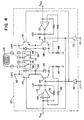
- the driver 122 is shown in greater detail in Figure 4, and it should be understood that driver 124 is essentially identical to it.
- a plurality of analog switches 126,128,130 and 132 Connected to the drivers 122 and 124 are a plurality of analog switches 126,128,130 and 132, each of which may be a dual SPOT switch, of type H15051, manufactured by Harris Semiconductor Analog Products Division, Melbourne, Florida. Operation of each of these switches is controlled by a bus 134, extending from the controller 110 to each switch.
- the analog switches 126, 128, 130, 132 are in turn connected to a plurality of coils 136, 138, 140 and 142 in a manner represented in Figure 5 by correspondingly numbered terminals and dashed lines such as lines 144, 146, 147 and 148.
- the collector of the transistor 154 is connected at 162 to a source of potential, shown as +28 volts DC, though some other suitable potential value such as +12 volts could be employed, with appropriate adjustment of other circuit parameters.
- the collector is also connected through the diode 158 to a node 164, from which one circuit path extends to one terminal of the switch 126.
- a second circuit path extends from the node 164 to the emitter of the transistor 154; a third circuit path extends from the node 164 to the collector of the transistor 156; and a fourth circuit path extends from the node 164 through the diode 160 to the emitter of the transistor 156 and through a current sensing 0.75-ohm, 2-watt resistor 166, to a base reference potential, shown as ground.
- the first logic input 112 is connected through an open collector gate 168, which may be of type 7407, to the base of the transistor 156 and to the base of a transistor 170 in the right circuit branch.
- the second logic input .114 is connected through an open collector gate 172, which may be of type 7407, to the base of the transistor 154 and to the base of a transistor 174 in the right circuit branch.
- the threshold voltage V TH1 from the converter 108 is applied to the positive input terminal of the comparator 150.
- the output of this comparator is connected to the base of the transistor 156, to which is also connected a potential of +5 volts through a 10,000-ohm pull-up resistor 176.
- a feedback path extends from the output of the comparator 150 through a 390,000- ohm resistor 178 to the positive input terminal thereof.
- the negative input terminal is connected through a 2,400-ohm resistor 180 to one end of the current sensing resistor 166.
- One terminal of the analog switch 128 is coupled via a conductor 182 to the right branch of the circuit of Figure 4, which includes the NPN transistors 170 and 174, diodes 184 and 186, a sense resistor 188 and the comparator 152.
- the various circuit paths connecting these components are similar to the corresponding circuit paths of the left branch, as may be seen from an inspection of Figure 4.
- the output of the comparator 150 goes negative, and causes the transistor 156 to turn off, thus interrupting the coil energizing circuit, and causing the current through the sensing resistor 166 to drop.
- controller 110 acting on the analog switches 126, 128, 130 and 132 through the bus 134, can selectively control the energization of coils 136, 138, 140 and 142, using only two drivers 122 and 124, thus reducing the number of components employed, to provide a more economical circuit configuration.
- the particular number of coils, switches and drivers shown is only exemplary, and other combinations could readily be used to provide configurations required in particular applications.
- FIG. 6 A further embodiment of the invention is shown in Figure 6.
- only one coil such as coil 190 or 192 of a predetermined number of coils, five in this example, is energized at any one time.
- Logic inputs 196 and 198 from a controller 189 are applied to the driver 194, which may be essentially identical to the driver of Figure 3.
- the outputs 200 and 202 of the driver are applied to terminals of two multiple-position switches 204 and 206 of suitable design, each of which is provided with a number of terminals 208 and 210 equal to the number of coils such as 190 and 192.
- a control bus 212 extending from the controller 189 to the switches 201 and 206 controls the simultaneous movement of said switches from one position to another, to provide the desired sequence of coil energization.
Landscapes
- Impact Printers (AREA)
Claims (10)
Applications Claiming Priority (2)
| Application Number | Priority Date | Filing Date | Title |
|---|---|---|---|
| US06/554,743 US4493253A (en) | 1983-11-23 | 1983-11-23 | Variable impact printing means |
| US554743 | 1983-11-23 |
Publications (3)
| Publication Number | Publication Date |
|---|---|
| EP0143575A2 EP0143575A2 (fr) | 1985-06-05 |
| EP0143575A3 EP0143575A3 (en) | 1986-01-08 |
| EP0143575B1 true EP0143575B1 (fr) | 1988-06-22 |
Family
ID=24214542
Family Applications (1)
| Application Number | Title | Priority Date | Filing Date |
|---|---|---|---|
| EP84307797A Expired EP0143575B1 (fr) | 1983-11-23 | 1984-11-12 | Mécanisme d'impression à pression de frappe variable et méthode |
Country Status (5)
| Country | Link |
|---|---|
| US (1) | US4493253A (fr) |
| EP (1) | EP0143575B1 (fr) |
| JP (1) | JPS60132778A (fr) |
| CA (1) | CA1215666A (fr) |
| DE (2) | DE143575T1 (fr) |
Families Citing this family (5)
| Publication number | Priority date | Publication date | Assignee | Title |
|---|---|---|---|---|
| US4806031A (en) * | 1986-08-15 | 1989-02-21 | Dataproducts Corporation | Uniform print density and registration in an impact printer |
| US5320435A (en) * | 1988-06-09 | 1994-06-14 | Datacard Corporation | Direct solenoid drive imprinting mechanism |
| US5237924A (en) * | 1990-11-30 | 1993-08-24 | Kabushiki Kaisha Shinkawa | Method of printing on workpieces of differing thicknesses |
| GB2252531B (en) * | 1991-01-08 | 1995-03-22 | Canon Business Machines Inc | Character printing device |
| US8576855B2 (en) | 2006-05-17 | 2013-11-05 | Alcatel Lucent | System and method of interface association for interface operational status event monitoring |
Family Cites Families (14)
| Publication number | Priority date | Publication date | Assignee | Title |
|---|---|---|---|---|
| US3172353A (en) * | 1963-06-17 | 1965-03-09 | Data Products Corp | Variable force hammer high speed printer |
| DE1237816B (de) * | 1963-08-24 | 1967-03-30 | Ibm Deutschland | Druckhammerantrieb fuer Schnelldrucker |
| BE699519A (fr) * | 1966-06-07 | 1967-11-16 | ||
| US3611783A (en) * | 1968-06-20 | 1971-10-12 | Hill Acme Co | Electromagnetically energized impact forming device |
| GB1275396A (en) * | 1969-03-13 | 1972-05-24 | Amp Inc | Electrodeposition of gold |
| BE755082A (fr) * | 1969-08-25 | 1971-02-01 | Ncr Co | Dispositif d'actionnement de marteaux d'impression |
| DE2033378B2 (de) * | 1970-07-06 | 1976-08-05 | Anker-Werke Ag, 4800 Bielefeld | Elektromagnetischer antrieb zur datenaufzeichnung |
| GB1331212A (en) * | 1971-04-15 | 1973-09-26 | Ibm | Electromagnetic actuator |
| US3741113A (en) * | 1971-06-25 | 1973-06-26 | Ibm | High energy print hammer unit with fast settle out |
| GB1382771A (en) * | 1972-01-11 | 1975-02-05 | Suwa Seikosha Kk | Control mechanism for a hammer of a printer and to a printer provided therewith |
| US4046244A (en) * | 1975-08-06 | 1977-09-06 | Sycor, Inc. | Impact matrix print head solenoid assembly |
| US4401026A (en) * | 1977-09-14 | 1983-08-30 | Exxon Reserach And Engineering Co. | Free flight hammer for impact printer |
| US4218150A (en) * | 1978-11-20 | 1980-08-19 | Vydec, Inc. | Matrix printer |
| EP0017918A1 (fr) * | 1979-04-16 | 1980-10-29 | Vydec, Inc. | Mécanisme d'impression et procédé pour imprimer des caractères alpha-numériques |
-
1983
- 1983-11-23 US US06/554,743 patent/US4493253A/en not_active Expired - Fee Related
-
1984
- 1984-09-26 CA CA000464025A patent/CA1215666A/fr not_active Expired
- 1984-11-12 DE DE198484307797T patent/DE143575T1/de active Pending
- 1984-11-12 DE DE8484307797T patent/DE3472233D1/de not_active Expired
- 1984-11-12 EP EP84307797A patent/EP0143575B1/fr not_active Expired
- 1984-11-21 JP JP59244731A patent/JPS60132778A/ja active Pending
Also Published As
| Publication number | Publication date |
|---|---|
| CA1215666A (fr) | 1986-12-23 |
| EP0143575A2 (fr) | 1985-06-05 |
| US4493253A (en) | 1985-01-15 |
| DE143575T1 (de) | 1985-10-10 |
| EP0143575A3 (en) | 1986-01-08 |
| DE3472233D1 (en) | 1988-07-28 |
| JPS60132778A (ja) | 1985-07-15 |
Similar Documents
| Publication | Publication Date | Title |
|---|---|---|
| CA1138803A (fr) | Circuit de commande a compensation des fluctuations de tension pour element de frappe d'imprimante | |
| US3866533A (en) | Electrical print impression control | |
| EP0603655B1 (fr) | Circuit de commande d'un solénoide à courant limité | |
| GB1391407A (en) | Stepping motor system | |
| US4503480A (en) | Voltage compensating driver circuit | |
| EP0143575B1 (fr) | Mécanisme d'impression à pression de frappe variable et méthode | |
| CA1210638A (fr) | Mecanisme a sonde opto-electronique et commande par microprocesseur | |
| US3628102A (en) | Exciter apparatus for impact member solenoid | |
| US4473311A (en) | Print wire drive assembly for dot-matrix printers | |
| US4048665A (en) | Driver circuit for printer electromagnet | |
| US5099383A (en) | Print head activating circuit for a wire dot printer | |
| US4556926A (en) | Electromagnet driving circuit | |
| US4015145A (en) | Voltage compensated timing circuit | |
| EP0387641B1 (fr) | Dispositif de réglage automatique de l'espacement pour tête d'impression | |
| EP0288864B1 (fr) | Circuit de commande pour tête d'impression par matrice de points | |
| CA1095584A (fr) | Circuit de commande de moteur pas-a-pas | |
| CA1065394A (fr) | Circuit d'attaque | |
| US4498791A (en) | Printer having improved stored energy printhead | |
| GB1570735A (en) | Solenoid drive circuit | |
| US4316056A (en) | Control circuit for electromagnetically-operated recorders in teleprinting devices | |
| US4812062A (en) | Print hammer with flux detection for print pressure control | |
| EP0017918A1 (fr) | Mécanisme d'impression et procédé pour imprimer des caractères alpha-numériques | |
| JP2680806B2 (ja) | 電磁式印字ヘツド駆動回路 | |
| EP0210074B1 (fr) | Appareil de triage | |
| US3754166A (en) | A driver circuit for actuating print wire solenoids |
Legal Events
| Date | Code | Title | Description |
|---|---|---|---|
| PUAI | Public reference made under article 153(3) epc to a published international application that has entered the european phase |
Free format text: ORIGINAL CODE: 0009012 |
|
| AK | Designated contracting states |
Designated state(s): DE FR GB |
|
| EL | Fr: translation of claims filed | ||
| DET | De: translation of patent claims | ||
| PUAL | Search report despatched |
Free format text: ORIGINAL CODE: 0009013 |
|
| AK | Designated contracting states |
Designated state(s): DE FR GB |
|
| 17P | Request for examination filed |
Effective date: 19860514 |
|
| 17Q | First examination report despatched |
Effective date: 19870715 |
|
| GRAA | (expected) grant |
Free format text: ORIGINAL CODE: 0009210 |
|
| AK | Designated contracting states |
Kind code of ref document: B1 Designated state(s): DE FR GB |
|
| REF | Corresponds to: |
Ref document number: 3472233 Country of ref document: DE Date of ref document: 19880728 |
|
| ET | Fr: translation filed | ||
| PLBE | No opposition filed within time limit |
Free format text: ORIGINAL CODE: 0009261 |
|
| STAA | Information on the status of an ep patent application or granted ep patent |
Free format text: STATUS: NO OPPOSITION FILED WITHIN TIME LIMIT |
|
| 26N | No opposition filed | ||
| PGFP | Annual fee paid to national office [announced via postgrant information from national office to epo] |
Ref country code: GB Payment date: 19900925 Year of fee payment: 7 |
|
| PGFP | Annual fee paid to national office [announced via postgrant information from national office to epo] |
Ref country code: FR Payment date: 19900928 Year of fee payment: 7 |
|
| PGFP | Annual fee paid to national office [announced via postgrant information from national office to epo] |
Ref country code: DE Payment date: 19901130 Year of fee payment: 7 |
|
| PG25 | Lapsed in a contracting state [announced via postgrant information from national office to epo] |
Ref country code: GB Effective date: 19911112 |
|
| GBPC | Gb: european patent ceased through non-payment of renewal fee | ||
| PG25 | Lapsed in a contracting state [announced via postgrant information from national office to epo] |
Ref country code: FR Effective date: 19920731 |
|
| PG25 | Lapsed in a contracting state [announced via postgrant information from national office to epo] |
Ref country code: DE Effective date: 19920801 |
|
| REG | Reference to a national code |
Ref country code: FR Ref legal event code: ST |