EP0143637B1 - Rückkopplungskammfilter - Google Patents
Rückkopplungskammfilter Download PDFInfo
- Publication number
- EP0143637B1 EP0143637B1 EP84308190A EP84308190A EP0143637B1 EP 0143637 B1 EP0143637 B1 EP 0143637B1 EP 84308190 A EP84308190 A EP 84308190A EP 84308190 A EP84308190 A EP 84308190A EP 0143637 B1 EP0143637 B1 EP 0143637B1
- Authority
- EP
- European Patent Office
- Prior art keywords
- circuit
- delay time
- delay
- signal
- comb filter
- Prior art date
- Legal status (The legal status is an assumption and is not a legal conclusion. Google has not performed a legal analysis and makes no representation as to the accuracy of the status listed.)
- Expired
Links
- 238000010586 diagram Methods 0.000 description 7
- 230000009897 systematic effect Effects 0.000 description 5
- 238000001914 filtration Methods 0.000 description 3
- 230000004048 modification Effects 0.000 description 2
- 238000012986 modification Methods 0.000 description 2
- 239000003990 capacitor Substances 0.000 description 1
- 238000010276 construction Methods 0.000 description 1
- 230000003111 delayed effect Effects 0.000 description 1
Images


Classifications
-
- H—ELECTRICITY
- H03—ELECTRONIC CIRCUITRY
- H03H—IMPEDANCE NETWORKS, e.g. RESONANT CIRCUITS; RESONATORS
- H03H11/00—Networks using active elements
- H03H11/02—Multiple-port networks
- H03H11/04—Frequency selective two-port networks
-
- H—ELECTRICITY
- H04—ELECTRIC COMMUNICATION TECHNIQUE
- H04N—PICTORIAL COMMUNICATION, e.g. TELEVISION
- H04N9/00—Details of colour television systems
- H04N9/77—Circuits for processing the brightness signal and the chrominance signal relative to each other, e.g. adjusting the phase of the brightness signal relative to the colour signal, correcting differential gain or differential phase
- H04N9/78—Circuits for processing the brightness signal and the chrominance signal relative to each other, e.g. adjusting the phase of the brightness signal relative to the colour signal, correcting differential gain or differential phase for separating the brightness signal or the chrominance signal from the colour television signal, e.g. using comb filter
Definitions
- the present invention generally relates to feedback type comb filters, and more particularly to a feedback type comb filter of a type having a feedback path for feeding back a part of an output of a delay circuit to an input of the delay circuit, which is designed so that a normal comb filter characteristic is obtained from a low-frequency range up to a high-frequency range.
- a conventional feedback type comb filter comprises a delay circuit for delaying an input signal, a first adding circuit for adding the input signal and an output signal of the delay circuit and for producing an output signal as an output of the comb filter, a second adding circuit for adding the input signal and the output signal of the first adding circuit, and a coefficient multiplier provided in a feedback path from the output of the first adding circuit to the second adding circuit see e.g. US ⁇ A ⁇ -3 836 707.
- a signal path is formed in which the input signal is applied to an input terminal, passed through the delay circuit, and is obtained through an output terminal.
- another signal path is formed in which the output signal of the delay circuit is passed through the coefficient multiplier, supplied to the delay circuit and passed through the delay circuit again, and is obtained through the output terminal.
- Another and more specific object of the present invention is to provide a feedback type comb filter in which a delay time of a main delay circuit is set to a time which is smaller than the delay time Tp of the delay circuit in the conventional feedback type comb filter by a delay time of a feedback loop which includes a coefficient multiplier, and a subsidiary delay circuit having a delay time approximately equal to the delay time of the feedback loop is provided in a stage prior to an adding circuit which adds an input signal and a fed back signal.
- a first signal path is formed in which the input signal is applied to an input terminal, passed through the subsidiary delay circuit and the main delay circuit, and is obtained through an output terminal.
- a second signal path is formed in which an output signal of the main delay circuit is passed through a feedback path including the coefficient multiplier, fed back to and passed through the main delay circuit, and is obtained through the output terminal.
- a delay time of the first signal path is equal to a delay time of the second signal path. Therefore, the peak frequencies of the pass bands assume the regular frequencies in all of the frequency bands, and it is possible to obtain a normal comb filter characteristic.
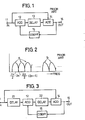
- a conventional feedback type comb filter has a circuit construction shown in Fig. 1, for example.
- An input video signal applied to an input terminal 11, is supplied to a delay circuit 13 through a first adding circuit 12.
- the input video signal is also supplied to a second adding circuit 14.
- the delay circuit 13 has a delay time Tp which is equal to one horizontal scanning period (1H) of the video signal, for example.
- An output delayed signal of the delay circuit 13 is added with the input video signal from the input terminal 11 in the second adding circuit 14.
- An output signal of the second adding circuit 14 is obtained through an output terminal 16.
- the output signal of the second adding circuit 14 is supplied to a coefficient multiplier 15 which multiplies a coefficient k to the signal.
- An output signal of the coefficient multiplier 15 is supplied to the first adding circuit 12 and is added with the input video signal from the input terminal 11.
- the conventional feedback type comb filter shown in Fig. 1 has a comb filter characteristic shown in Fig. 2.
- center frequencies of the attenuation bands are equal to odd number multiples of F p /2, that is, (2n + 1) times F p /2.
- the delay time Tp is equal to a time period of 1 H
- the frequency Fp is equal to the horizontal scanning frequency, and in this case, a luminance signal within the input video signal is separated and obtained through the output terminal 16.
- a signal path is formed in which the input video signal is applied to the input terminal 11, passed through the first adding circuit 12, the delay circuit 13, and the second adding circuit 14, and is obtained through the output terminal 16.
- another signal path is formed in which the output signal of the second delay circuit 14 is passed through the coefficient multiplier 15, the first adding circuit 12, the delay circuit 13, and the second adding circuit 14, and is obtained through the output terminal 16.
- comb filter characteristics a in the relatively low-frequency range are close to the normal comb filter characteristics.
- the distortions in the comb filter characteristics in the high-frequency range become greater in the high-frequency range.
- comb filter characteristics b are greatly distorted from the normal comb filter characteristics.
- Fig. 3 is a systematic block diagram showing an embodiment of the feedback type comb filter according to the present invention.
- those parts which are the same as those corresponding parts in Fig. 1 are designated by the same reference numerals, and their description will be omitted.
- a main delay circuit 22 corresponding to the delay circuit 13 which is coupled between the first and second adders 12 and 14 in the conventional feedback type comb filter, has a delay time T H .
- the delay time T H is smaller than a predetermined time Tp by a delay time T2 of a feedback loop which extends from the output of the second adding circuit 14, passes through the coefficient multiplier 15, and reaches the input of the first adding circuit 12.
- a subsidiary delay circuit 21 is coupled betwen the input terminal 11 and the first adding circuit 12, so as to delay the input video signal by a delay time ⁇ 1 .
- Fig. 4 is an equivalent circuit diagram showing delay factors in the feedback type comb filter shown in Fig. 3.
- the delay time ⁇ 1 of a delay factor 31 represents the delay time of the subsidiary delay circuit 21.
- the delay time T H of a delay factor 32 represents the delay time of the main delay circuit 22.
- the delay time T2 of the delay factor 33 represents the delay time of the feedback path including the coefficient multiplier 15.
- a delay time ⁇ 3 of a delay factor 34 represents the delay time of the feedback path including the coefficient multiplier 15.
- a delay time ⁇ 3 of a delay factor 34 represents the delay time of the signal path from the input terminal 11 directly to the second adding circuit 14.
- a comb filter characteristic shown in Fig. 5(A) is obtained.
- the center frequencies of the pass bands are even number multiples of (that is, 2n times) the frequency 1/[2(T H + T i )], are equal to n/(T H + T i -On the other hand, the center frequencies of the attenuation bands are odd number multiples of (that is, (2n +w 1) times) the frequency 1/[2(T H + T,)].
- the maximum level is "2"
- the minimum level is "0" in the comb filter characteristic shown in Fig. (5A).
- An interval between the center frequencies of two adjacent pass bands is equal to 1/(T H + T I ).
- the delay times are used in the description given above, however, an inverse number of the time indicates the frequency.
- the horizontal axis represents the frequency.
- a characteristic shown in Fig. 5(B) is obtained.
- the center frequencies of the pass bands are even number multiples of 1/[(T H + T l )], and are equal to n/[2(t H + T f )].
- the center frequencies of the attenuation bands are odd number multiples of 1/[2(T H + T,)].
- the maximum level is 1/(1 - k), and the minimum level is 1/(1 + k).
- the characteristics of the transfer function described by the equation (3) is a product of the two characteristics shown in Figs. 5(A) and 5(B). For this reason, in a case where the center frequencies n/ (T H + T I ) and n/(T H + T, of the pass bands in the two characterstics do not coincide, the charactersitic of the transfer function described by the equation (3) becomes shown in Fig. 5(C).
- Figs. 5(A) through 5(C) in the case where the center frequencies of the pass bands in the two characteristics shown in Figs. 5(A) and 5(B) do not coincide, the peak frequencies of the pass bands in the characteristic shift from the center frequencies of the pass bands as shown in FIG. 5(A). As a result, the characteristic shown in Fig. 5(C) is non-symmetrical about the center frequencies of the pass bands, and the characterstic is distorted compared to the original characteristic which is symmetrical about the center frequencies of the pass bands.
- a characteristic shown in Fig. (5)E is obtained as a product of the two characteristics shown in Figs. 5(A) and 5(D).
- the characteristic is symmetrical about the center frequencies of the pass bands and is symmetrical about the center frequencies of the attenuation bands.
- the characteristic shown in Fig. 5(E) is a normal comb filter characteristic.
- the condition described by the following equation (5) must be satisfied, because it is necessary to obtain a comb filter characteristic in which the center frequencies of the pass bands are even number multiples of 1/2H and the center frequencies of the attenuation bands are odd number multiples of 1/2(2H).
- the center frequencies of the pass bands become equal to even number multiples of f H /2, that is, equal to n ⁇ f H .
- the center frequencies of the attenuation bands become equal to odd number multiples of f H /2, that is, equal to (2n + 1) ⁇ f H /2.
- the delay time ⁇ 1 of the subsidiary delay circuit 21 may be selected to a value which is approximately equal to the delay time T2 of the feedback path.
- FIG. 6 An embodiment of a concrete circuit of the feedback type comb filter shown in Fig. 3, will now be described by referring to Fig. 6.
- Fig. 6 those parts which are the same as those corresponding parts in Fig. 3 are designated by the same reference numerals.
- the subsidiary delay circuit 21 comprises a delay circuit 41 and resistors R 1 and R 2 .
- the delay circuit 41 comprises coils L 1 and L 2 , capacitors C 1 and C 2 , and a transformer TR.
- the first adding circuit 12 comprises an adder 42.
- the main delay circuit 22 comprises a charge coupled device (CCD) 43, a clock pulse generator 44 for supplying a clock pulse to the CCD 43, and a lowpass filter 45 for eliminating a clock component which is mixed into an output signal of the CCD 43.
- the second adding circuit 14 comprises an adder 46.
- An attenuator 47 is provided in a signal path between the input terminal 11 and the second adding circuit 14, so as to match the levels of the signals which are added in the second adding circuits 14.
- the coefficent multiplier 15 which is coupled between the output of the second adding circuit 14 and the input of the first adding circuit 12, comprises a variable resistor 48 which may be variably adjusted so that the coefficient k becomes equal to 0.5 for example, and an amplifier 49.
- the delay time T3 of the signal path which starts from the input terminal 11 and reaches the input of the second adding circuit 14 through the attenuator 47 is approximately equal to zero.
- the delay time ⁇ 2 of the coefficient multiplier 15 is approximately equal to 20 nano-seconds (nsecs).
- the constants of the circuit elements constituting the delay circuit 41 of the subsidiary delay circuit 21 are selected to values so that the delay time ⁇ 1 of the subsidiary delay circuit 21 is approximately equal to 20 nsec.
- the delay time T H of the main delay circuit 22 is selected to (1 H - 20 nsec).
- the delay times ⁇ 1 and T2 respectively assume values which are in the range of several tens of nsec.
- the object of the present invention may also be achieved when a non-linear circuit such as a limiter circuit, or a frequency selecting circuit such as a highpass filter and a bandpass filter, is coupled to the coefficient multiplier 15 according to the needs.
- a substracting circuit 51 shown in Fig. 7 is used instead of the second adding circuit 14 shown in Fig. 3.
- An adding circuit may be used for the substracting circuit 51, by inverting the polarity of an input signal to one of two input terminals of the subtracting circuit 51.
Landscapes
- Engineering & Computer Science (AREA)
- Multimedia (AREA)
- Signal Processing (AREA)
- Processing Of Color Television Signals (AREA)
- Filters That Use Time-Delay Elements (AREA)
Claims (5)
Applications Claiming Priority (2)
| Application Number | Priority Date | Filing Date | Title |
|---|---|---|---|
| JP222709/83 | 1983-11-26 | ||
| JP58222709A JPS60114017A (ja) | 1983-11-26 | 1983-11-26 | 帰還型くし形フイルタ |
Publications (3)
| Publication Number | Publication Date |
|---|---|
| EP0143637A2 EP0143637A2 (de) | 1985-06-05 |
| EP0143637A3 EP0143637A3 (en) | 1987-04-01 |
| EP0143637B1 true EP0143637B1 (de) | 1990-08-16 |
Family
ID=16786673
Family Applications (1)
| Application Number | Title | Priority Date | Filing Date |
|---|---|---|---|
| EP84308190A Expired EP0143637B1 (de) | 1983-11-26 | 1984-11-26 | Rückkopplungskammfilter |
Country Status (4)
| Country | Link |
|---|---|
| US (1) | US4617588A (de) |
| EP (1) | EP0143637B1 (de) |
| JP (1) | JPS60114017A (de) |
| DE (2) | DE143637T1 (de) |
Families Citing this family (3)
| Publication number | Priority date | Publication date | Assignee | Title |
|---|---|---|---|---|
| JPS61121574A (ja) * | 1984-11-19 | 1986-06-09 | Hitachi Ltd | ビデオ信号処理回路 |
| JP3228800B2 (ja) * | 1992-11-11 | 2001-11-12 | 株式会社日立製作所 | モータ制御装置およびこれを用いた磁気記録再生装置 |
| GB0117090D0 (en) * | 2001-07-12 | 2001-09-05 | Kvaerner Process Tech Ltd | Process |
Family Cites Families (5)
| Publication number | Priority date | Publication date | Assignee | Title |
|---|---|---|---|---|
| US3707596A (en) * | 1969-12-19 | 1972-12-26 | Philips Corp | Circuit arrangement for surpressing the chrominance subcarrier in pal signal |
| US3836707A (en) * | 1971-12-27 | 1974-09-17 | Hitachi Ltd | Video signal processing device for extracting the chrominance and luminance signals from a composite video signal in a color television receiver |
| JPS5860888A (ja) * | 1981-10-08 | 1983-04-11 | Toshiba Corp | 色分離回路 |
| US4498100A (en) * | 1982-11-26 | 1985-02-05 | Rca Corporation | Apparatus for frame-to-frame comb filtering composite TV signal |
| US4553158A (en) * | 1984-02-06 | 1985-11-12 | Rca Corporation | Circuitry for correcting motion induced errors in frame comb filtered video signals |
-
1983
- 1983-11-26 JP JP58222709A patent/JPS60114017A/ja active Pending
-
1984
- 1984-11-26 DE DE198484308190T patent/DE143637T1/de active Pending
- 1984-11-26 EP EP84308190A patent/EP0143637B1/de not_active Expired
- 1984-11-26 DE DE8484308190T patent/DE3482988D1/de not_active Expired - Lifetime
- 1984-11-26 US US06/674,544 patent/US4617588A/en not_active Expired - Lifetime
Also Published As
| Publication number | Publication date |
|---|---|
| US4617588A (en) | 1986-10-14 |
| DE3482988D1 (de) | 1990-09-20 |
| DE143637T1 (de) | 1985-10-24 |
| EP0143637A2 (de) | 1985-06-05 |
| JPS60114017A (ja) | 1985-06-20 |
| EP0143637A3 (en) | 1987-04-01 |
Similar Documents
| Publication | Publication Date | Title |
|---|---|---|
| EP0478377B1 (de) | Schaltungen zur Kompensation des horizontalen Randes | |
| PL124517B1 (en) | Apparatus for processing of electric signals | |
| US4646153A (en) | Noise reduction circuit for a video signal | |
| US4488251A (en) | Digital filter | |
| EP0331017B1 (de) | Schaltung zur Einstellung der Bildqualität mit einem FIR-Filter zur digitalen Verarbeitung | |
| EP0143637B1 (de) | Rückkopplungskammfilter | |
| JPS6322760B2 (de) | ||
| US5157362A (en) | Narrow band notch filter with extended passband | |
| EP1708488A2 (de) | Bildbearbeitungsvorrichtung | |
| EP0613310B1 (de) | Trennschaltung für Leuchtdichte-Farbsignale | |
| EP0122096B1 (de) | Chrominanz-invertierendes Allpassfilter | |
| EP0254512A2 (de) | Vorrichtung zum Aufzeichnen und Wiedergeben für ein Videosignal | |
| EP0506055A2 (de) | Verzerrungsgerät | |
| US6987542B2 (en) | Detection and correction of asymmetric transient signals | |
| US4635119A (en) | Integrated circuit of a digital filter for the luminance channel of a color-television receiver | |
| JPS5994986A (ja) | クロマ信号用集積化デジタルフイルタ装置 | |
| EP0147073B1 (de) | Schaltung zur Rauschverminderung für ein Videosignal | |
| US5422679A (en) | Video signal processor for removing a separated signal component from an input video signal | |
| EP0232597B1 (de) | Schaltung zur Verarbeitung des Luminanzsignals | |
| RU2166231C2 (ru) | Устройство компенсации помех для приемников широкополосных фазоманипулированных сигналов | |
| JPH0137027B2 (de) | ||
| EP0009537B1 (de) | Ein Kammfilter | |
| DE3240905A1 (de) | Digitale signaltrennschaltung | |
| JPH053197B2 (de) | ||
| JP3184376B2 (ja) | 周波数自動調整回路 |
Legal Events
| Date | Code | Title | Description |
|---|---|---|---|
| PUAI | Public reference made under article 153(3) epc to a published international application that has entered the european phase |
Free format text: ORIGINAL CODE: 0009012 |
|
| AK | Designated contracting states |
Designated state(s): DE FR GB |
|
| EL | Fr: translation of claims filed | ||
| 17P | Request for examination filed |
Effective date: 19850815 |
|
| DET | De: translation of patent claims | ||
| PUAL | Search report despatched |
Free format text: ORIGINAL CODE: 0009013 |
|
| AK | Designated contracting states |
Kind code of ref document: A3 Designated state(s): DE FR GB |
|
| 17Q | First examination report despatched |
Effective date: 19891221 |
|
| GRAA | (expected) grant |
Free format text: ORIGINAL CODE: 0009210 |
|
| AK | Designated contracting states |
Kind code of ref document: B1 Designated state(s): DE FR GB |
|
| ET | Fr: translation filed | ||
| REF | Corresponds to: |
Ref document number: 3482988 Country of ref document: DE Date of ref document: 19900920 |
|
| PLBE | No opposition filed within time limit |
Free format text: ORIGINAL CODE: 0009261 |
|
| STAA | Information on the status of an ep patent application or granted ep patent |
Free format text: STATUS: NO OPPOSITION FILED WITHIN TIME LIMIT |
|
| 26N | No opposition filed | ||
| REG | Reference to a national code |
Ref country code: GB Ref legal event code: IF02 |
|
| PGFP | Annual fee paid to national office [announced via postgrant information from national office to epo] |
Ref country code: FR Payment date: 20031110 Year of fee payment: 20 |
|
| PGFP | Annual fee paid to national office [announced via postgrant information from national office to epo] |
Ref country code: GB Payment date: 20031126 Year of fee payment: 20 |
|
| PGFP | Annual fee paid to national office [announced via postgrant information from national office to epo] |
Ref country code: DE Payment date: 20031204 Year of fee payment: 20 |
|
| PG25 | Lapsed in a contracting state [announced via postgrant information from national office to epo] |
Ref country code: GB Free format text: LAPSE BECAUSE OF EXPIRATION OF PROTECTION Effective date: 20041125 |
|
| REG | Reference to a national code |
Ref country code: GB Ref legal event code: PE20 |