EP0144143B1 - Schaltungsanordnung zur Steuerung der Lautstärke - Google Patents
Schaltungsanordnung zur Steuerung der Lautstärke Download PDFInfo
- Publication number
- EP0144143B1 EP0144143B1 EP19840307351 EP84307351A EP0144143B1 EP 0144143 B1 EP0144143 B1 EP 0144143B1 EP 19840307351 EP19840307351 EP 19840307351 EP 84307351 A EP84307351 A EP 84307351A EP 0144143 B1 EP0144143 B1 EP 0144143B1
- Authority
- EP
- European Patent Office
- Prior art keywords
- signal
- digital
- audio signal
- sound volume
- multiplier
- Prior art date
- Legal status (The legal status is an assumption and is not a legal conclusion. Google has not performed a legal analysis and makes no representation as to the accuracy of the status listed.)
- Expired
Links
- 230000005236 sound signal Effects 0.000 claims description 43
- 238000010586 diagram Methods 0.000 description 3
- 239000003990 capacitor Substances 0.000 description 1
Images
Classifications
-
- H—ELECTRICITY
- H03—ELECTRONIC CIRCUITRY
- H03G—CONTROL OF AMPLIFICATION
- H03G3/00—Gain control in amplifiers or frequency changers
- H03G3/002—Control of digital or coded signals
-
- H—ELECTRICITY
- H03—ELECTRONIC CIRCUITRY
- H03G—CONTROL OF AMPLIFICATION
- H03G1/00—Details of arrangements for controlling amplification
- H03G1/0005—Circuits characterised by the type of controlling devices operated by a controlling current or voltage signal
- H03G1/0088—Circuits characterised by the type of controlling devices operated by a controlling current or voltage signal using discontinuously variable devices, e.g. switch-operated
-
- H—ELECTRICITY
- H03—ELECTRONIC CIRCUITRY
- H03G—CONTROL OF AMPLIFICATION
- H03G1/00—Details of arrangements for controlling amplification
- H03G1/04—Modifications of control circuit to reduce distortion caused by control
-
- H—ELECTRICITY
- H03—ELECTRONIC CIRCUITRY
- H03G—CONTROL OF AMPLIFICATION
- H03G3/00—Gain control in amplifiers or frequency changers
Definitions
- This invention relates generally to audio signal processing, and particularly to a circuit arrangement for adjusting sound volume of an input audio signal.
- US-A-4. 270 177 discloses a digital amplitude control unit in which an analogue control signal is converted to a digital signal by an A/D converter, which digital signal is then multiplied with the audio information to produce the desired output amplitude.
- the present invention has been developed in order to reduce the above-described drawbacks inherent to the conventional sound volume adjusting apparatus.
- a circuit arrangement for sound volume adjustment including: a multipler responsive to an input audio signal for adjusting the amplitude of said audio signal by performing multiplication such that said audio is multiplied by a variable control signal; a manipulative portion for producing said variable control signal indicative of an intended sound volume of said audio signal; and an analogue-to-digital converter for converting said variable control signal into a digital control signal to be fed to said multiplier, characterized in that it further comprises:
- the invention enables provision of a circuit arrangement for sound volume adjusting which suffers less from the occurrence of click noise on gain control.
- an instant where an instantaneous value of an input audio signal to be controlled becomes zero or nearly zero is detected by way of a zero detector, and a digital signal to be fed to a multiplier functioning as a gain control circuit is updated or renewed in response to an output signal from the zero detector so that gain is changed when the instantaneous value of the input audio signal is very small.
- Patent Abstracts of Japan, vol. 4, No. 87 (E-16) [569], 21st June 1980, referring to JP-A-5552613 discloses a circuit whereby latching of a new, single-bit value is only permitted at, or near signal zero, thus permitting transient-free on/off switching of an audio signal.
- An audio signal whose amplitude is to be controlled for sound volume adjustment may be an analog signal or a digital signal, and the present invention is applicable to either cases.
- an input audio signal which is either an analog signal or a digital signal, is multipled by a digital signal representing an intended sound volume.
- the present invention is adapted to such a sound volume adjusting circuit using a multiplier.
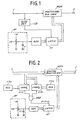
- the first embodiment circuit arrangement is used for processing an analog audio signal, while the second embodiment circuit arrangement is used for processing a digital audio signal.
- the reference 1 is an input terminal for an audio signal which is to be controlled and is an objective of sound volume control
- the reference 2 is an output terminal of an audio signal whose sound volume has been controlled.
- the reference OP is a manipulative portion for sound volume adjustment;
- ADC an A/D converter;
- LC a latch;
- ZD a zero detector which is arranged to produce an output signal when the instantaneous value of the audio signal to be controlled is low and is within a predetermined range close to zero.
- the reference MDA in Fig. 1 is a multiplying digital-to-analog (D/A) converter
- the reference MPY in Fig. 2 is a digital multiplier.
- the multiplying D/A converter MDA is a D/A converter having an input terminal for receiving a varying reference voltage.
- the multiplying D/A converter may be used an integrated circuit known as AD1408 or AD1508 manufactured by Analog Devices, Inc.
- the digital multiplier may be used an integrated circuit known as ADSP-1012 also manufactured by Analog Devices, Inc.
- manipulative portion OP is shown to be constructed of a variable resistor VR and a capacitor C, it is a matter of course that the manipulative portion OP can have other structure when practicing the present invention.
- a digital signal indicative of an intended sound volume may be separately produced by way of an external circuit, and such an external digital signal may be directly applied to the latch LC.
- a digital signal outputted from the above-mentioned A/D converter ADC is fed to the latch LC. Then the latch LC receives the digital signal fed from the A/D converter ADC to the latch LC and at an instant where an output signal from the zero detector ZD is applied thereto, holds the digital signal.
- the output signal from the above-mentioned latch LC is fed to the multiplying D/A converter MDA in the first embodiment of Fig. 1, and to the digital multiplier MPY in the second embodiment of Fig. 2.
- the analog signal fed from the input terminal 1 is multiplied by the digital signal outputted from the latch LC so as to output a signal to the output terminal 2, which output signal is in a state that the sound volume of the audio signal fed to the input terminal 1, having an analog signal form, has been adjusted in accordance with the manipulation in the manipulative portion OP.
- the digital signal fed from the input terminal 1 is multipled by the digital signal outputted from the latch LC so as to output a signal to the output terminal 2, which output signal is in a state that the sound volume of the audio signal fed to the input terminal 1, having a digital signal form, has been adjusted in accordance with the manipulation in the manipulative portion OP.
- an instant where the latch LC receives and holds a digital signal from the A/ D converter ADC is an instant where a signal from the zero detector ZD is applied thereto
- the instant where a signal is applied from the zero detector ZD is an instant where the instantaneous value of the audio signal fed to the input terminal 1 as an objective of sound volume adjustment in the apparatus according to the present invention is at zero or close thereto.
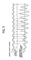
- Fig. 3 is a timing chart for the description of the operation of the sound volume adjusting apparatus according to the present invention.
- the audio signal fed to the input terminal 1 as an objective of sound volume adjustment, the output signal from the zero detector ZD, and the output signal of the multiplying D/A converter MDA are shown. Since the zero detector ZD produces an output pulse signal each time the instantaneous value of the input audio signal equals zero, the latch LC responsive to the output signal from the zero detector ZD is controlled so that digital data indicative of intended sound volume from the A/D converter ADC is latched in the presence of the output signal from the zero detector ZD.
- This digital data latched in the latch LC is not changed until subsequent output signal from the zero detector ZD is applied, and is fed to the multiplying D/A converter MDA for sound volume control.
- the movable contact of the variable resistor VR of the manipulative portion OP has been manipulated to change a demand for sound volume.
- An analog voltage fed to the A/D converter ADC is changed and digital output fed to the latch LC is changed accordingly.
- This changed digital data will be referred to as new digital data or signal.
- the instant that the latch LC receives and holds the new digital signal from the A/D converter ADC, namely, the instant where the amplitude of the audio signal is actually changed.
- the zero detector ZD may be used known or well known circuits which are capable of producing an output signal when an instantaneous value of an audio signal is low and is within a predetermined range close to zero.
- the zero detector ZD shown in Fig. 2 is an example which handles a digital signal.
- the references COMPu and COMPd are comparators; PSu and PSd, registers; AND, an AND gate.
- a numerical value u is set in the register PSu, while another numerical value d is set in the other register PSd where u>d.
- the comparator COMPu produces an output signal when a numerical value X having a relationship of u>X with respect to the numerical value u set in the register PSu is inputted, while the other comparator COMPd produces an output signal when a numerical value X having a relationship of X>d with respect to the numerical value d set in the register PSd is inputted.
- the signal from the AND gate AND is fed to the latch LC only when the numerical value X of the audio signal fed to the input terminal 1 as an objective of sound volume adjustment is low and is within a predetermined range close to zero, and then the latch LC receives and holds the new digital signal from the A/D converter ADC so that the amplitude of the audio signal is changed by the sound volume adjustment.
- the present invention provides a sound volume adjusting apparatus of the type arranged to vary transfer gain of an audio signal in a stepwise manner, comprising means for varying transfer gain of said audio signal when an instantaneous value of said audio signal to be controlled is low and is within a predetermined range close to zero, an instant where the amplitude of an audio signal is actually changed is set at a time in which the instantaneous value of the audio signal fed to the input terminal 1 as an objective of sound volume adjustment is low and is within a predetermined range close to zero, and therefore, click noise does not occur during sound volume adjustment in the sound volume adjusting apparatus according to the present invention.
- the above-mentioned problem inherentto the conventional apparatus is satisfactorily resolved according to the present invention apparatus.
Landscapes
- Control Of Amplification And Gain Control (AREA)
Claims (4)
Applications Claiming Priority (2)
| Application Number | Priority Date | Filing Date | Title |
|---|---|---|---|
| JP20240983A JPS6094513A (ja) | 1983-10-28 | 1983-10-28 | 音量調整装置 |
| JP202409/83 | 1983-10-28 |
Publications (3)
| Publication Number | Publication Date |
|---|---|
| EP0144143A2 EP0144143A2 (de) | 1985-06-12 |
| EP0144143A3 EP0144143A3 (en) | 1986-05-07 |
| EP0144143B1 true EP0144143B1 (de) | 1990-01-03 |
Family
ID=16457023
Family Applications (1)
| Application Number | Title | Priority Date | Filing Date |
|---|---|---|---|
| EP19840307351 Expired EP0144143B1 (de) | 1983-10-28 | 1984-10-25 | Schaltungsanordnung zur Steuerung der Lautstärke |
Country Status (4)
| Country | Link |
|---|---|
| EP (1) | EP0144143B1 (de) |
| JP (1) | JPS6094513A (de) |
| AU (1) | AU553037B2 (de) |
| DE (1) | DE3480980D1 (de) |
Cited By (1)
| Publication number | Priority date | Publication date | Assignee | Title |
|---|---|---|---|---|
| CN103701419B (zh) * | 2013-12-06 | 2016-08-24 | 乐视致新电子科技(天津)有限公司 | 一种音量调节方法及装置 |
Families Citing this family (9)
| Publication number | Priority date | Publication date | Assignee | Title |
|---|---|---|---|---|
| FI92778C (fi) * | 1986-09-24 | 1994-12-27 | Rca Licensing Corp | Digitaalisignaalin amplitudinsäätöjärjestelmä digitaalisignaalien muuttamiseksi jokseenkin tasaisin dB-askelin |
| FR2621189A1 (fr) * | 1987-09-25 | 1989-03-31 | Rustin Serge | Dispositif pour la reduction des bruits parasites dans les applications d'attenuateurs d'amplificateurs commandes numeriquement |
| JP2591656B2 (ja) * | 1988-06-14 | 1997-03-19 | パイオニア株式会社 | 音量・音質調整装置 |
| JPH0812979B2 (ja) * | 1989-11-21 | 1996-02-07 | 日本電気株式会社 | 自動利得制御装置 |
| JPH04148562A (ja) * | 1990-10-12 | 1992-05-21 | Kawasaki Steel Corp | 集積回路 |
| JP3604927B2 (ja) * | 1998-11-17 | 2004-12-22 | パイオニア株式会社 | オーディオ信号処理装置 |
| JP4712510B2 (ja) * | 2005-10-11 | 2011-06-29 | 学校法人関東学院 | 熱交換用既製杭の設置方法、熱交換用既製杭の造成方法および底部用既製杭 |
| US9425747B2 (en) | 2008-03-03 | 2016-08-23 | Qualcomm Incorporated | System and method of reducing power consumption for audio playback |
| US8717211B2 (en) | 2010-11-30 | 2014-05-06 | Qualcomm Incorporated | Adaptive gain adjustment system |
Family Cites Families (7)
| Publication number | Priority date | Publication date | Assignee | Title |
|---|---|---|---|---|
| DD131608B1 (de) * | 1977-07-15 | 1981-03-25 | Reinhard Adam | Digitaler steller mit verringerten stoerungen beim stel |
| JPS5552613A (en) * | 1978-10-13 | 1980-04-17 | Sanyo Electric Co Ltd | Sound control circuit |
| NL8003027A (nl) * | 1979-05-29 | 1980-12-02 | Analog Devices Inc | Signaal-bestuurbare verzwakker met een digitaal/- analoogomvormer. |
| US4270177A (en) * | 1979-06-20 | 1981-05-26 | Tokyo Shibaura Denki Kabushiki Kaisha | Digital amplitude control for digital audio signal |
| DE2926011C2 (de) * | 1979-06-27 | 1984-10-18 | Tokyo Shibaura Denki K.K., Kawasaki, Kanagawa | Digitale Amplituden-Steuerschaltung |
| JPS5728409A (en) * | 1980-07-28 | 1982-02-16 | Sony Corp | Muting circuit |
| NL8100033A (nl) * | 1981-01-07 | 1982-08-02 | Philips Nv | Signaaloverdrachtsinrichting met een in stappen instelbare overdrachtskarakteristiek. |
-
1983
- 1983-10-28 JP JP20240983A patent/JPS6094513A/ja active Pending
-
1984
- 1984-10-23 AU AU34592/84A patent/AU553037B2/en not_active Ceased
- 1984-10-25 DE DE8484307351T patent/DE3480980D1/de not_active Expired - Fee Related
- 1984-10-25 EP EP19840307351 patent/EP0144143B1/de not_active Expired
Cited By (1)
| Publication number | Priority date | Publication date | Assignee | Title |
|---|---|---|---|---|
| CN103701419B (zh) * | 2013-12-06 | 2016-08-24 | 乐视致新电子科技(天津)有限公司 | 一种音量调节方法及装置 |
Also Published As
| Publication number | Publication date |
|---|---|
| EP0144143A2 (de) | 1985-06-12 |
| AU3459284A (en) | 1985-05-09 |
| JPS6094513A (ja) | 1985-05-27 |
| DE3480980D1 (de) | 1990-02-08 |
| AU553037B2 (en) | 1986-07-03 |
| EP0144143A3 (en) | 1986-05-07 |
Similar Documents
| Publication | Publication Date | Title |
|---|---|---|
| US4999628A (en) | Analog-to-digital converting unit with broad dynamic range | |
| EP0144143B1 (de) | Schaltungsanordnung zur Steuerung der Lautstärke | |
| EP0351788B1 (de) | Analog-Digitalwandlersystem | |
| CA1191614A (en) | Analog to digital conversion method and apparatus | |
| EP0112115A1 (de) | Übertragungssystem für Sensoren | |
| GB2060293A (en) | Analogue to digital converter system with an output stabilizing circuit | |
| US4498072A (en) | A/D Converter having a self-bias circuit | |
| EP0065795B1 (de) | DA-Wandler für bipolare Signale | |
| US4544918A (en) | Analog-to-digital conversion circuit | |
| US5257301A (en) | Direct digital frequency multiplier | |
| GB2087181A (en) | Amplifier circuit with output level correction | |
| EP0076009B1 (de) | Abstimmvorrichtung mit einer Frequenzsynthesierschaltung | |
| US4351032A (en) | Frequency sensing circuit | |
| US5311314A (en) | Method of and arrangement for suppressing noise in a digital signal | |
| EP0180971A2 (de) | Impulsformerschaltung | |
| EP0261848B1 (de) | Klangfarbenregelung für bemusterte Daten | |
| JPH0145254B2 (de) | ||
| JPS588614B2 (ja) | キジユンデンイセイギヨカイロ | |
| GB2098420A (en) | Conversion between analogue and digital signals | |
| JP2723614B2 (ja) | ディジタル制御位相同期発振器の自走周波数制御方式 | |
| JP2556723B2 (ja) | 量子化器 | |
| US4470019A (en) | Rate multiplier square root extractor with increased accuracy for transmitter applications | |
| SU1151999A1 (ru) | Устройство дл воспроизведени дробно-рациональных функций | |
| JPS63260208A (ja) | デジタルagc方式 | |
| JP2617484B2 (ja) | 逐次比較型a−d変換器 |
Legal Events
| Date | Code | Title | Description |
|---|---|---|---|
| PUAI | Public reference made under article 153(3) epc to a published international application that has entered the european phase |
Free format text: ORIGINAL CODE: 0009012 |
|
| AK | Designated contracting states |
Designated state(s): DE FR GB |
|
| PUAL | Search report despatched |
Free format text: ORIGINAL CODE: 0009013 |
|
| AK | Designated contracting states |
Kind code of ref document: A3 Designated state(s): DE FR GB |
|
| 17P | Request for examination filed |
Effective date: 19861031 |
|
| 17Q | First examination report despatched |
Effective date: 19880810 |
|
| GRAA | (expected) grant |
Free format text: ORIGINAL CODE: 0009210 |
|
| AK | Designated contracting states |
Kind code of ref document: B1 Designated state(s): DE FR GB |
|
| REF | Corresponds to: |
Ref document number: 3480980 Country of ref document: DE Date of ref document: 19900208 |
|
| ET | Fr: translation filed | ||
| PLBE | No opposition filed within time limit |
Free format text: ORIGINAL CODE: 0009261 |
|
| STAA | Information on the status of an ep patent application or granted ep patent |
Free format text: STATUS: NO OPPOSITION FILED WITHIN TIME LIMIT |
|
| 26N | No opposition filed | ||
| PGFP | Annual fee paid to national office [announced via postgrant information from national office to epo] |
Ref country code: FR Payment date: 19931011 Year of fee payment: 10 |
|
| PGFP | Annual fee paid to national office [announced via postgrant information from national office to epo] |
Ref country code: GB Payment date: 19931015 Year of fee payment: 10 |
|
| PGFP | Annual fee paid to national office [announced via postgrant information from national office to epo] |
Ref country code: DE Payment date: 19931021 Year of fee payment: 10 |
|
| PG25 | Lapsed in a contracting state [announced via postgrant information from national office to epo] |
Ref country code: GB Effective date: 19941025 |
|
| GBPC | Gb: european patent ceased through non-payment of renewal fee |
Effective date: 19941025 |
|
| PG25 | Lapsed in a contracting state [announced via postgrant information from national office to epo] |
Ref country code: FR Effective date: 19950630 |
|
| PG25 | Lapsed in a contracting state [announced via postgrant information from national office to epo] |
Ref country code: DE Effective date: 19950701 |
|
| REG | Reference to a national code |
Ref country code: FR Ref legal event code: ST |