EP0144182A2 - Filtres transmettant la lumière - Google Patents
Filtres transmettant la lumière Download PDFInfo
- Publication number
- EP0144182A2 EP0144182A2 EP84307941A EP84307941A EP0144182A2 EP 0144182 A2 EP0144182 A2 EP 0144182A2 EP 84307941 A EP84307941 A EP 84307941A EP 84307941 A EP84307941 A EP 84307941A EP 0144182 A2 EP0144182 A2 EP 0144182A2
- Authority
- EP
- European Patent Office
- Prior art keywords
- light
- filter
- base plate
- transmitting
- layer
- Prior art date
- Legal status (The legal status is an assumption and is not a legal conclusion. Google has not performed a legal analysis and makes no representation as to the accuracy of the status listed.)
- Withdrawn
Links
Images

Classifications
-
- C—CHEMISTRY; METALLURGY
- C03—GLASS; MINERAL OR SLAG WOOL
- C03C—CHEMICAL COMPOSITION OF GLASSES, GLAZES OR VITREOUS ENAMELS; SURFACE TREATMENT OF GLASS; SURFACE TREATMENT OF FIBRES OR FILAMENTS MADE FROM GLASS, MINERALS OR SLAGS; JOINING GLASS TO GLASS OR OTHER MATERIALS
- C03C17/00—Surface treatment of glass, not in the form of fibres or filaments, by coating
- C03C17/22—Surface treatment of glass, not in the form of fibres or filaments, by coating with other inorganic material
-
- C—CHEMISTRY; METALLURGY
- C03—GLASS; MINERAL OR SLAG WOOL
- C03C—CHEMICAL COMPOSITION OF GLASSES, GLAZES OR VITREOUS ENAMELS; SURFACE TREATMENT OF GLASS; SURFACE TREATMENT OF FIBRES OR FILAMENTS MADE FROM GLASS, MINERALS OR SLAGS; JOINING GLASS TO GLASS OR OTHER MATERIALS
- C03C17/00—Surface treatment of glass, not in the form of fibres or filaments, by coating
- C03C17/06—Surface treatment of glass, not in the form of fibres or filaments, by coating with metals
-
- G—PHYSICS
- G02—OPTICS
- G02B—OPTICAL ELEMENTS, SYSTEMS OR APPARATUS
- G02B5/00—Optical elements other than lenses
-
- G—PHYSICS
- G02—OPTICS
- G02B—OPTICAL ELEMENTS, SYSTEMS OR APPARATUS
- G02B5/00—Optical elements other than lenses
- G02B5/20—Filters
- G02B5/205—Neutral density filters
-
- C—CHEMISTRY; METALLURGY
- C03—GLASS; MINERAL OR SLAG WOOL
- C03C—CHEMICAL COMPOSITION OF GLASSES, GLAZES OR VITREOUS ENAMELS; SURFACE TREATMENT OF GLASS; SURFACE TREATMENT OF FIBRES OR FILAMENTS MADE FROM GLASS, MINERALS OR SLAGS; JOINING GLASS TO GLASS OR OTHER MATERIALS
- C03C2217/00—Coatings on glass
- C03C2217/20—Materials for coating a single layer on glass
-
- C—CHEMISTRY; METALLURGY
- C03—GLASS; MINERAL OR SLAG WOOL
- C03C—CHEMICAL COMPOSITION OF GLASSES, GLAZES OR VITREOUS ENAMELS; SURFACE TREATMENT OF GLASS; SURFACE TREATMENT OF FIBRES OR FILAMENTS MADE FROM GLASS, MINERALS OR SLAGS; JOINING GLASS TO GLASS OR OTHER MATERIALS
- C03C2217/00—Coatings on glass
- C03C2217/20—Materials for coating a single layer on glass
- C03C2217/25—Metals
- C03C2217/257—Refractory metals
- C03C2217/26—Cr, Mo, W
-
- C—CHEMISTRY; METALLURGY
- C03—GLASS; MINERAL OR SLAG WOOL
- C03C—CHEMICAL COMPOSITION OF GLASSES, GLAZES OR VITREOUS ENAMELS; SURFACE TREATMENT OF GLASS; SURFACE TREATMENT OF FIBRES OR FILAMENTS MADE FROM GLASS, MINERALS OR SLAGS; JOINING GLASS TO GLASS OR OTHER MATERIALS
- C03C2217/00—Coatings on glass
- C03C2217/20—Materials for coating a single layer on glass
- C03C2217/25—Metals
- C03C2217/27—Mixtures of metals, alloys
-
- C—CHEMISTRY; METALLURGY
- C03—GLASS; MINERAL OR SLAG WOOL
- C03C—CHEMICAL COMPOSITION OF GLASSES, GLAZES OR VITREOUS ENAMELS; SURFACE TREATMENT OF GLASS; SURFACE TREATMENT OF FIBRES OR FILAMENTS MADE FROM GLASS, MINERALS OR SLAGS; JOINING GLASS TO GLASS OR OTHER MATERIALS
- C03C2217/00—Coatings on glass
- C03C2217/20—Materials for coating a single layer on glass
- C03C2217/28—Other inorganic materials
- C03C2217/287—Chalcogenides
- C03C2217/289—Selenides, tellurides
-
- C—CHEMISTRY; METALLURGY
- C03—GLASS; MINERAL OR SLAG WOOL
- C03C—CHEMICAL COMPOSITION OF GLASSES, GLAZES OR VITREOUS ENAMELS; SURFACE TREATMENT OF GLASS; SURFACE TREATMENT OF FIBRES OR FILAMENTS MADE FROM GLASS, MINERALS OR SLAGS; JOINING GLASS TO GLASS OR OTHER MATERIALS
- C03C2218/00—Methods for coating glass
- C03C2218/30—Aspects of methods for coating glass not covered above
- C03C2218/32—After-treatment
- C03C2218/328—Partly or completely removing a coating
Definitions
- This invention relates to methods of producing light-transmitting filters suitable for luminance correction purposes in an exposure device for producing a phosphor screen of a cathode ray tube, and to light-transmitting filters produced by such methods.
- light-transmitting filters having different light transmittance in different portions of the filter, and preset distribution characteristics of transmitted light may be produced.
- a phosphor slurry is applied to the inner surface of the panel of a cathode ray tube.
- the slurry coating is exposed to a light beam by an exposure device making use of a light-transmitting filter, and is then developed.
- the light-transmitting filter used in the exposure device there are known various methods, for example, photographic methods, transcription methods, and methods of sequentially combining small pieces of different light transmittance.
- a master pattern consisting of the reverse pattern of the light-transmitting filter to be produced is prepared by a plotter and transcribed onto a photographic dry plate having a higher gamma value.
- the step of producing the master pattern is omitted and a pattern consisting of a combination of stripes of variable width is formed on a photographic dry plate with a higher gamma value, by exposing the dry plate to a light beam whose intensity is modulated by means of an interposed rotary plate.
- the pattern thus formed on the dry plate is developed and fixed.
- a glass plate coated with a photoresist layer is intimately applied to the photographic dry plate. After exposure, a carbon slurry is poured on the glass plate.
- the pattern is transcribed to the carbon mass to form the light-transmitting filter having the preset light transmittance distribution characteristics.
- This method has the deficiency that several steps are required, so that the manufacturing time can generally not be reduced. Moreover, it is difficult with this method to produce the light transmitting filter with higher accuracy because of the error caused during the steps of preparation of the master pattern, exposure of the photographic dry plate, development/fixing and transcription to and development of the carbon slurry coating.
- a method of producing a selective light-transmitting filter comprising the steps of:
- a light-transmitting filter produced in this way may be used for example in an exposure device for the preparation of a phosphor screen of a high definition colour cathode ray tube with high definition and fidelity.
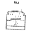
- FIG. 1 there is shown an exposure device employed for instance for the preparation of a phosphor screen of a cathode ray tube.
- the device has a light-transmitting filter 1 and a light source 2 formed by an ultrahigh-voltage mercury lamp provided with a forced air cooling system.
- a phosphor slurry 6 formed on the inner surface of a panel 5 of the cathode ray tube is exposed to the light L emitted by the light source 2 and passed through a correction lens 3, and thereby sensitized in accordance with a pattern set by a colour selective electrode 4.
- the phosphor slurry 6 consists of a phosphor material dispersed into a resin of the type cured by ultraviolet rays.
- the phosphor slurry 6 thus exposed to the light and thereby sensitized is subjected to a developing step.
- the phosphorescent screen can be formed on the inner surface of the panel 5 of the cathode ray tube by repetition of the above described operation for each of the three colour phosphors.
- the planar light-transmitting filter 1 is arranged below the correction lens 3, the function of which is to cause the exposure light path to coincide with the trajectory of the electron beam.
- the filter 1 is placed within the exposure device for illuminance compensation in such a manner that the phosphor slurry coating is exposed at the correct positions of the dots or stripes to be formed on the phosphor screen, and the dots or stripes are formed with a uniform configuration on the overall phosphor screen.
- the light emitted by the light source 2 is an ultraviolet light having a wavelength of, for example, 3650 angstroms
- the filter 1 needs to be fabricated of a material that is not decomposed by the ultraviolet rays.
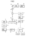
- FIG. 2 is a block diagram of a device for carrying out the process for the preparation of a light-transmitting filter.
- the filter prepared by this device is used for example in the above-described exposure device.
- the distribution of the light directed to the phosphor slurry coating for exposure may be corrected to an optimum value, so that the configuration of the phosphor dots or stripes that make up the phosphor screen of the colour cathode ray tube is rendered uniform on the overall phosphor screen surface.
- the surface of the filter base plate on which a thin film of heat mode optical recording medium is formed is irradiated by a laser beam for selectively evaporating the thin film and forming a pattern of light transmitting through-holes, so that a light-transmitting filter with predetermined light transmittance distribution may be prepared in a short time and with high accuracy.
- the laser beam is modulated with a light modulator under the command of a computer unit.
- the filter base plate is secured to a stage which is movable in X-Y directions under the command of the computer unit.
- FIG. 2 there is shown a CAD device for the preparation of the light-transmitting filter with the aid of a computer system.
- a stage 13 on which a light modulator 11 and a filter base plate 12 are mounted, and which is movable in X and Y directions is controlled by a computer unit 10.
- the signals corresponding to the desired light transmittance distribution of the light-transmitting filter to be prepared are read out from a signal input device or reader 14 and entered into the computer unit 10.
- the output data from the computer unit 10 are supplied to an interface circuit 15 where they are converted into control signals which are used for controlling the light modulator 11.
- These control signals are then supplied to a signal level converter 16 where they are converted for example into transistor-transistor logic (TTL) level signals.
- TTL transistor-transistor logic
- the output signals from the signal level converter 16 are supplied to a drive circuit 17 where they are converted to voltage signals capable of directly driving the light modulator 11.
- the output data from the computer unit 10 are also supplied to an interface circuit 18 where they are converted into control signals for controlling the movement of the stage 13 in the X-direction (transverse direction) and the Y-direction (vertical direction).
- These control signals are then supplied to a signal level converter 19 where they are converted for example into TTL signal levels.
- the output signals from the signal level converter 19 are then supplied to an encoder 20 where they are encoded and translated into signals capable of driving a linear motor 21, which is thereby activated for controlling the movement of the movable stage 13 at a rate of for example 200 to 1000 mm/sec.
- the output data from the computer unit 10 are also supplied to a plotter 22 for delineating, for example, a characteristic curve showing the light transmittance distribution of the light-transmitting filter being produced by the device shown in Figure 2.
- the filter base plate 12 which is transparent and formed, for example, of glass, is securely mounted on the stage 13. To the overall surface of the filter base plate 12, there is applied a layer, for example, of tellurium (Te) to a thickness for example of 1000 to 1500 angstroms by, for example, vacuum deposition, for providing a thin layer 12A of opaque heat mode optical recording material.
- Te tellurium
- the filter base plate 12 is used per se as the light transmitting filter in the exposure device shown in Figure 1, the filter base plate 12 is preferably fabricated of glass which is low in alkaline content, such as quartz glass or acrylic resin (PMMA) in order that the base plate is not discoloured by the ultraviolet rays in the exposure device and can be used for a prolonged time.
- An argon gas laser with, for example, a rated output of four watts is used as the laser light source 24 to which an exciting current is supplied from a stabilized power source 23.
- the argon laser is highly stable and the laser output has a stability of about 0.2 percent related to the time elapsed.
- a krypton laser, which is equally stable, may be used instead of the argon laser.
- the laser beam R which is supplied from the laser light source 24 and consisting of the fundamental TEMoo mode with a uniform beam intensity distribution is reflected by a mirror 25 and condensed within the light modulator 11 by a first lens 25.
- the light modulator 11 makes use of acousto-optic cells (AO cells) or electro-optic cells (EO cells), and the light passing through the light modulator 11 can be deflected towards left and right by the crystal lattice of the piezo-optical crystals becoming deformed under the applied voltage.
- AO cells acousto-optic cells
- EO cells electro-optic cells
- the laser light R is modulated or turned on and off at a rate of 10 -6 to 10-10 sec when passing through the light modulator 11 which makes use of, for example, EO cells and to which the signal voltage is applied from the drive circuit 17.
- the primary mode laser beam which has passed through the light modulator 11 and which accounts for about 50 percent of the total laser beam is collected by a second lens 27, and the laser beam of the multiple longitudinal modes is irradiated on the thin layer 12A of the filter base plate 12.
- the thin layer 12A is selectively vapourized in these spots so as to form light- emitting through-holes.
- the light modulator 11 is controlled by the computer unit 10 at this time, while the stage 13 on which the filter base plate 12 is securely mounted is moved in both the X and Y directions under the command of the computer unit 10, so that a pattern of the through-holes indicative of the preset light transmittance distribution is formed on the filter base plate 12.
- FIGs 3 and 4 there is shown a relationship between the through-holes formed on the filter base plate 12 and the pulse signals applied to the light modulator 11.
- the through-holes shown at A are formed on the filter base plate 12.
- the through-hole shown at A in Figure 3 is constant in width W but variable in length D depending on the pulse width Tw of the applied signal. It is thus seen that the preset light transmittance distribution can be realised on the filter base plate 12 by forming a pattern of the through-holes with variable lengths D on the base plate 12.
- the through-holes formed on the filter base plate 12 may be changed in density instead of in duration depending upon the voltage signal shown at B in Figure 4.
- the diameter S of each through-hole is the same, but the density of distribution of the through-holes is variable so that the preset light transmittance distribution may be realised on the filter base plate 12.
- the thin layer 12A obtained by vacuum deposition on the filter base plate 12 is poor in mechanical strength and suceptible to damage. It is also chemically unstable and can be oxidized easily. For this reason, a protective film for the thin layer 12A may be provided, or a glass plate or the like may be affixed to the surface of the filter base plate 12 by means of an optical adhesive. In this manner, a light-transmitting filter can be provided which is immune to opto-chemical reaction and able to withstand the irradiation of ultraviolet rays in the exposure device for the preparation of the phosphor screen.
- this light-transmitting filter is prepared by the two steps of irradiation with laser light beam and the formation of the protective coating for the thin layer, the number of the process steps can be reduced as compared with the conventional process.
- a light-transmitting filter used for example for producing phosphor stripes at intervals of 0.2 mm on the phosphor screen can be prepared in one to two hours, whereas five to six hours were required in the preparation of the same filter with the conventional system.
- the intensity of the exposure light of the photographic dry plate was varied with the use of a rotary disc for providing a pattern of variable stripe widths.
- the intensity of the laser light radiated on the surface of the filter base plate 12 is maintained constant and the pulse width Tw of the voltage applied to the light modulator 11 is changed for changing the length D of the through-holes formed on the base plate 12.
- the diameter D of the through-holes may be kept constant and the distribution of through-hole density may be changed by pulse number modulation for realising the preset light transmittance distribution on the filter base plate.
- the rotary plate for which a sufficient accuracy can generally not be expected, is dispensed with, and the laser light is modulated by the light modulator 11 operating accurately in response to the input signal in such a manner the length D or the density of the through-holes is changed and the desired light transmittance distribution can be accurately and faithfully reproduced on the filter base plate 12.
- the accuracy in the light transmittance of 1 to 2% heretofore possible at the photographic developing stage can be raised to 0.2 to 3%.
- tellurium is used for the formation of the thin layer 12A of the heat mode optical recording material.
- chromium can be deposited to a thickness of 1000 to 2000 angstroms for the formation of the thin layer 12A.
- the filter base plate 12 should be formed of glass, micro-sized cracks are liable to develop in the glass due to heat stress when the metallized film is irradiated with the laser light. This is because the chromium (Cr) has a higher boiling point than tellurium (Te). Therefore in this case the filter base plate is preferably formed of quartz glass.
- TeCu TeCu
- TeC AsTe
- TeSe TeSeTe
- TeOx tellurium oxide
- As 2 Se 3 Se
- CuPc cupro-phthalo-cyanine
- Bi Bi or Ni
- the present invention can be applied to the preparation not only of light-transmitting filters used in exposure devices for phosphor screens, but to light-transmitting filters used for other purposes.
- the width of the light transmitting through-holes is maintained constant and the length D thereof is changed, or alternatively, the diameter S of the through-holes is maintained constant and the density of the through-holes is generally changed.
- the desired preset light transmittance may also be achieved by changing the intensity of the laser beam or by changing the width of the light-transmitting stripes by means of an appropriate optical control system.
Landscapes
- Chemical & Material Sciences (AREA)
- Physics & Mathematics (AREA)
- Chemical Kinetics & Catalysis (AREA)
- Life Sciences & Earth Sciences (AREA)
- Optics & Photonics (AREA)
- Engineering & Computer Science (AREA)
- General Physics & Mathematics (AREA)
- General Chemical & Material Sciences (AREA)
- Geochemistry & Mineralogy (AREA)
- Materials Engineering (AREA)
- Organic Chemistry (AREA)
- Formation Of Various Coating Films On Cathode Ray Tubes And Lamps (AREA)
- Exposure And Positioning Against Photoresist Photosensitive Materials (AREA)
- Optical Filters (AREA)
Applications Claiming Priority (2)
| Application Number | Priority Date | Filing Date | Title |
|---|---|---|---|
| JP58223894A JPS60136703A (ja) | 1983-11-28 | 1983-11-28 | 光透過フィルタの製造方法 |
| JP223894/83 | 1983-11-28 |
Publications (2)
| Publication Number | Publication Date |
|---|---|
| EP0144182A2 true EP0144182A2 (fr) | 1985-06-12 |
| EP0144182A3 EP0144182A3 (fr) | 1987-09-02 |
Family
ID=16805368
Family Applications (1)
| Application Number | Title | Priority Date | Filing Date |
|---|---|---|---|
| EP84307941A Withdrawn EP0144182A3 (fr) | 1983-11-28 | 1984-11-15 | Filtres transmettant la lumière |
Country Status (3)
| Country | Link |
|---|---|
| US (1) | US4803337A (fr) |
| EP (1) | EP0144182A3 (fr) |
| JP (1) | JPS60136703A (fr) |
Cited By (2)
| Publication number | Priority date | Publication date | Assignee | Title |
|---|---|---|---|---|
| EP0706067A1 (fr) * | 1994-09-07 | 1996-04-10 | Kureha Kagaku Kogyo Kabushiki Kaisha | Filtre optique plastique |
| US5672655A (en) * | 1994-09-13 | 1997-09-30 | Kureha Kagaku Kogyo Kabushiki Kaisha | Plastic optical material and production process thereof |
Families Citing this family (2)
| Publication number | Priority date | Publication date | Assignee | Title |
|---|---|---|---|---|
| US5308180A (en) * | 1991-12-09 | 1994-05-03 | Minnesota Mining And Manufacturing Company | Liquid applicator with metering insert |
| US5729393A (en) * | 1996-04-03 | 1998-03-17 | Digital Papyrus Corporation | Optical flying head with solid immersion lens having raised central surface facing medium |
Family Cites Families (12)
| Publication number | Priority date | Publication date | Assignee | Title |
|---|---|---|---|---|
| DE1292470B (de) * | 1965-03-30 | 1969-04-10 | Steigerwald Strahltech | Verfahren zur Materialbearbeitung mittels Strahlungsenergie |
| US3622742A (en) * | 1970-05-27 | 1971-11-23 | Bell Telephone Labor Inc | Laser machining method and apparatus |
| GB1441745A (en) * | 1972-10-06 | 1976-07-07 | Emi Ltd | Manufacture of a pattern on a substrate |
| US4316073A (en) * | 1974-11-14 | 1982-02-16 | Lemelson Jerome H | Document recording method |
| DE2458370C2 (de) * | 1974-12-10 | 1984-05-10 | Dr.-Ing. Rudolf Hell Gmbh, 2300 Kiel | Energiestrahl-Gravierverfahren und Einrichtung zu seiner Durchführung |
| DE2511390C2 (de) * | 1975-03-15 | 1984-03-15 | Agfa-Gevaert Ag, 5090 Leverkusen | Verfahren und Vorrichtung zur Herstellung von Tageslichtprojektionsschirmen sowie nach diesem Verfahren hergestellter Tageslichtprojektionsschirm |
| US4087281A (en) * | 1975-09-19 | 1978-05-02 | Rca Corporation | Method of producing optical image on chromium or aluminum film with high-energy light beam |
| US4131782A (en) * | 1976-05-03 | 1978-12-26 | Lasag Ag | Method of and apparatus for machining large numbers of holes of precisely controlled size by coherent radiation |
| GB1562093A (en) * | 1976-10-13 | 1980-03-05 | Hitachi Ltd | Light intesity distribution correcting filter and manufacturing mehtod of the same |
| US4465540A (en) * | 1979-05-03 | 1984-08-14 | Albert Richard D | Method of manufacture of laminate radiation collimator |
| US4297559A (en) * | 1979-05-10 | 1981-10-27 | Olin Corporation | Apparatus for controlled perforation of moving webs with fixed focus laser beam |
| US4386145A (en) * | 1980-10-01 | 1983-05-31 | Eastman Kodak Company | Fabrication of arrays containing interlaid patterns of microcells |
-
1983
- 1983-11-28 JP JP58223894A patent/JPS60136703A/ja active Pending
-
1984
- 1984-11-15 EP EP84307941A patent/EP0144182A3/fr not_active Withdrawn
-
1987
- 1987-11-25 US US07/125,828 patent/US4803337A/en not_active Expired - Fee Related
Cited By (2)
| Publication number | Priority date | Publication date | Assignee | Title |
|---|---|---|---|---|
| EP0706067A1 (fr) * | 1994-09-07 | 1996-04-10 | Kureha Kagaku Kogyo Kabushiki Kaisha | Filtre optique plastique |
| US5672655A (en) * | 1994-09-13 | 1997-09-30 | Kureha Kagaku Kogyo Kabushiki Kaisha | Plastic optical material and production process thereof |
Also Published As
| Publication number | Publication date |
|---|---|
| US4803337A (en) | 1989-02-07 |
| JPS60136703A (ja) | 1985-07-20 |
| EP0144182A3 (fr) | 1987-09-02 |
Similar Documents
| Publication | Publication Date | Title |
|---|---|---|
| US3856525A (en) | Method for manufacturing cathode ray tube screen | |
| US3891440A (en) | Process for fabricating a color cathode ray tube screen structure incorporating optical filter means therein | |
| EP0144182A2 (fr) | Filtres transmettant la lumière | |
| US4021239A (en) | Method of exposing parallel stripe-like areas on photosensitive member | |
| US3779760A (en) | Method of producing a striped cathode ray tube screen | |
| US3834905A (en) | Method of making elliptically or rectangularly graded photoprinting masters | |
| JP2542179B2 (ja) | カラ―画像複製方法 | |
| US4696879A (en) | Method for exposing a color tri-cathode ray tube panel to form three separate color phosphor stripe patterns by exposure from three separate light source positions using combination of corrective lenses | |
| JP3280774B2 (ja) | カラー受像管用蛍光面形成方法及び露光装置 | |
| JP2003337428A (ja) | 露光装置 | |
| US4045224A (en) | Method for making phosphor screen for black matrix type color picture tube using two light sources | |
| US4248947A (en) | Method for master pattern production | |
| US3875627A (en) | Method of manufacturing a target plate for a color television camera tube | |
| JPH05120993A (ja) | 露光光源装置 | |
| JPS60119055A (ja) | カラ−陰極線管の製法 | |
| JP2615832B2 (ja) | 光ディスク原盤製造方法 | |
| JPH09293675A (ja) | 周辺露光装置 | |
| JPS6217925A (ja) | 露光方法 | |
| GB2176647A (en) | Manufacture of colour CRT phosphor screens | |
| US4488793A (en) | Photodepositing a CRT screen structure using discrete-element optical filter | |
| RU2106966C1 (ru) | Источник модулированного излучения | |
| JPH1140053A (ja) | カラー陰極線管とその製造方法 | |
| JPH07249378A (ja) | 補正レンズ及びその製造方法並びにこの補正レンズを用いた露光装置及びその露光方法 | |
| WO1990010047A1 (fr) | Fabrication de plaques a cablage imprime par imagerie par projection | |
| JPH03206437A (ja) | 光情報処理装置 |
Legal Events
| Date | Code | Title | Description |
|---|---|---|---|
| PUAI | Public reference made under article 153(3) epc to a published international application that has entered the european phase |
Free format text: ORIGINAL CODE: 0009012 |
|
| AK | Designated contracting states |
Designated state(s): DE FR GB |
|
| PUAL | Search report despatched |
Free format text: ORIGINAL CODE: 0009013 |
|
| AK | Designated contracting states |
Kind code of ref document: A3 Designated state(s): DE FR GB |
|
| 17P | Request for examination filed |
Effective date: 19880126 |
|
| 17Q | First examination report despatched |
Effective date: 19890929 |
|
| STAA | Information on the status of an ep patent application or granted ep patent |
Free format text: STATUS: THE APPLICATION IS DEEMED TO BE WITHDRAWN |
|
| 18D | Application deemed to be withdrawn |
Effective date: 19900210 |
|
| RIN1 | Information on inventor provided before grant (corrected) |
Inventor name: KIMURA, TOMOHIROC/O PATENT DEPARTMENT Inventor name: ISHIKAWA, REIJIC/O PATENT DEPARTMENT |