EP0144444A1 - Herstellungsverfahren für halbleitervorrichtung - Google Patents
Herstellungsverfahren für halbleitervorrichtung Download PDFInfo
- Publication number
- EP0144444A1 EP0144444A1 EP84902071A EP84902071A EP0144444A1 EP 0144444 A1 EP0144444 A1 EP 0144444A1 EP 84902071 A EP84902071 A EP 84902071A EP 84902071 A EP84902071 A EP 84902071A EP 0144444 A1 EP0144444 A1 EP 0144444A1
- Authority
- EP
- European Patent Office
- Prior art keywords
- layer
- forming
- semiconductor device
- manufacturing
- semiconductive
- Prior art date
- Legal status (The legal status is an assumption and is not a legal conclusion. Google has not performed a legal analysis and makes no representation as to the accuracy of the status listed.)
- Granted
Links
Images




Classifications
-
- H—ELECTRICITY
- H10—SEMICONDUCTOR DEVICES; ELECTRIC SOLID-STATE DEVICES NOT OTHERWISE PROVIDED FOR
- H10P—GENERIC PROCESSES OR APPARATUS FOR THE MANUFACTURE OR TREATMENT OF DEVICES COVERED BY CLASS H10
- H10P76/00—Manufacture or treatment of masks on semiconductor bodies, e.g. by lithography or photolithography
- H10P76/40—Manufacture or treatment of masks on semiconductor bodies, e.g. by lithography or photolithography of masks comprising inorganic materials
-
- H—ELECTRICITY
- H10—SEMICONDUCTOR DEVICES; ELECTRIC SOLID-STATE DEVICES NOT OTHERWISE PROVIDED FOR
- H10D—INORGANIC ELECTRIC SEMICONDUCTOR DEVICES
- H10D10/00—Bipolar junction transistors [BJT]
- H10D10/40—Vertical BJTs
- H10D10/441—Vertical BJTs having an emitter-base junction ending at a main surface of the body and a base-collector junction ending at a lateral surface of the body
-
- H—ELECTRICITY
- H10—SEMICONDUCTOR DEVICES; ELECTRIC SOLID-STATE DEVICES NOT OTHERWISE PROVIDED FOR
- H10D—INORGANIC ELECTRIC SEMICONDUCTOR DEVICES
- H10D48/00—Individual devices not covered by groups H10D1/00 - H10D44/00
- H10D48/30—Devices controlled by electric currents or voltages
- H10D48/32—Devices controlled by only the electric current supplied, or only the electric potential applied, to an electrode which does not carry the current to be rectified, amplified or switched
- H10D48/34—Bipolar devices
- H10D48/345—Bipolar transistors having ohmic electrodes on emitter-like, base-like, and collector-like regions
-
- Y—GENERAL TAGGING OF NEW TECHNOLOGICAL DEVELOPMENTS; GENERAL TAGGING OF CROSS-SECTIONAL TECHNOLOGIES SPANNING OVER SEVERAL SECTIONS OF THE IPC; TECHNICAL SUBJECTS COVERED BY FORMER USPC CROSS-REFERENCE ART COLLECTIONS [XRACs] AND DIGESTS
- Y10—TECHNICAL SUBJECTS COVERED BY FORMER USPC
- Y10S—TECHNICAL SUBJECTS COVERED BY FORMER USPC CROSS-REFERENCE ART COLLECTIONS [XRACs] AND DIGESTS
- Y10S148/00—Metal treatment
- Y10S148/026—Deposition thru hole in mask
-
- Y—GENERAL TAGGING OF NEW TECHNOLOGICAL DEVELOPMENTS; GENERAL TAGGING OF CROSS-SECTIONAL TECHNOLOGIES SPANNING OVER SEVERAL SECTIONS OF THE IPC; TECHNICAL SUBJECTS COVERED BY FORMER USPC CROSS-REFERENCE ART COLLECTIONS [XRACs] AND DIGESTS
- Y10—TECHNICAL SUBJECTS COVERED BY FORMER USPC
- Y10S—TECHNICAL SUBJECTS COVERED BY FORMER USPC CROSS-REFERENCE ART COLLECTIONS [XRACs] AND DIGESTS
- Y10S148/00—Metal treatment
- Y10S148/05—Etch and refill
-
- Y—GENERAL TAGGING OF NEW TECHNOLOGICAL DEVELOPMENTS; GENERAL TAGGING OF CROSS-SECTIONAL TECHNOLOGIES SPANNING OVER SEVERAL SECTIONS OF THE IPC; TECHNICAL SUBJECTS COVERED BY FORMER USPC CROSS-REFERENCE ART COLLECTIONS [XRACs] AND DIGESTS
- Y10—TECHNICAL SUBJECTS COVERED BY FORMER USPC
- Y10S—TECHNICAL SUBJECTS COVERED BY FORMER USPC CROSS-REFERENCE ART COLLECTIONS [XRACs] AND DIGESTS
- Y10S148/00—Metal treatment
- Y10S148/103—Mask, dual function, e.g. diffusion and oxidation
-
- Y—GENERAL TAGGING OF NEW TECHNOLOGICAL DEVELOPMENTS; GENERAL TAGGING OF CROSS-SECTIONAL TECHNOLOGIES SPANNING OVER SEVERAL SECTIONS OF THE IPC; TECHNICAL SUBJECTS COVERED BY FORMER USPC CROSS-REFERENCE ART COLLECTIONS [XRACs] AND DIGESTS
- Y10—TECHNICAL SUBJECTS COVERED BY FORMER USPC
- Y10S—TECHNICAL SUBJECTS COVERED BY FORMER USPC CROSS-REFERENCE ART COLLECTIONS [XRACs] AND DIGESTS
- Y10S148/00—Metal treatment
- Y10S148/106—Masks, special
Definitions
- This invention relates to a method for manufacturing a semiconductor device, particularly an IC . device of a bipolar transistor.
- Fig. 1 is a cross-sectional view of a main part of a bipolar transistor IC that is manufactured by using the selective oxidation method.
- reference numeral 1 designates a silicon semiconductor substrate of, for example, P type.
- Reference numeral 2 designates a collector embedded layer of N type
- reference numeral 3 designates a collector region formed of an N type epitaxial growth layer
- reference numeral 4 designates a base region
- reference numeral 5 designates an emitter region
- reference numeral 6 designates an Si0 2 layer formed by the selective oxidation method
- reference numeral 7 designates a portion from which a collector electrode is led out.
- Reference letters C, E and B respectively designate terminal for the collector, emitter and base.
- the selective oxidation process for manufacturing this bipolar transistor IC has the following problems. That is, if a bird's beak (the bird's beak protrudes to approximately lu) and a bird's head are generated as shown in Fig.
- the mask alignments are respectively necessary; in this case, the tolerance including the alignment precision and the bird's beak is necessary; since the spacing between the base electrode leading-out portion and the emitter electrode leading-out portion is determined by the tolerance of the Al electrode, there is a limit to make the spacing narrow; the parasitic capacity of the collector is considerably affected by the region except the active region (so-called intrinsic portion); and the above problems give a limit on making the cell size smaller, etc.
- a manufacturing method for producing a bipolar transistor IC as shown in Fig. 2 (refer to Japanese patent application No. 62701/1983).
- an N + type collector embedded layer 2 is formed first in a silicon semiconductive substrate 1 of, for example, P type.
- window apertures 9 and 10 are selectively formed-through predetermined portions of the insulating film, for example, an SiO 2 film 8 on the major surface of the substrate, namely, the portions corresponding to the active region and the collector electrode leading-out portion of the transistor.
- the whole surface including the Si0 2 film 8 and the window apertures 9 and 10 is subjected to the vapor phase growth treatment, whereby a single crystal silicon 16 is formed within the window apertures 9 and 10 and a polycrystalline silicon 17 is formed on the Si0 2 layer 8. Thereafter, the single crystal silicon 16 and the polycrystalline silicon 17 are flattened and the polycrystalline silicon 17 is selectively removed. Then, formed on the single crystalline silicon 16 within the window aperture 9 are an N - type collector region 3, a P type base region 4 and an N + type emitter region 5 and the polycrystalline silicon 17 is made as the base electrode lead-out portion, while formed on the single crystalline silicon 16 within the other window aperture 10 is an N + type collector electrode lead-out portion, thus a bipolar transistor IC being formed.
- this invention to provide a method for manufacturing a semiconductor device capable of solving the problem of the separation between the elements caused by the selective oxidation method and in which the respective collector, base and - emitter regions and the emitter electrode lead-out portions are formed in the self-alignment fashion so as to permit the elements to be more smaller and an IC device of high efficiency and high integration density can be manufactured.
- This invention relates to a method for manufacturing a semiconductor device which comprises the steps of forming a semiconductive layer having on its surface formed a concave portion, forming a nitride layer within this concave portion, forming an oxide layer on a surface of the semiconductive layer with the nitride layer as a mask, removing this nitride layer and introducing an impurity into the semiconductive layer with the oxide layer as a mask.
- the element can be made finer and it is possible to obtain the IC device of high efficiency and high integration density.
- Figs. 1 and 2 are cross-sectional views of bipolar transistors manufactured by a prior art manufacturing method
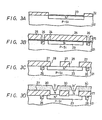
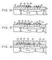
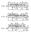
- Figs. 3A to 3M are cross-sectional views of an embodiment of this invention in process order
- Fig. 4 is an enlarged cross-sectional view of a main part useful for explaining this invention.
- FIG. 3 An embodiment of a method for manufacturing a semiconductor device according to this invention will hereinafter be described with reference to Fig. 3.
- the present invention is applied to an NPN transistor, but it is needless to say that this invention can also be applied to a PNP-transistor.
- an oxide layer (SiO 2 ) 22 is formed on a P type silicon semiconductive substrate 21
- a window is formed through this oxide layer 22 and an N type impurity is diffused into the substrate 21 through the window so as to form an N type collector embedded layer 23.
- a thin oxide layer (Si0 2 ) 24 is formed in place thereof. While a photo resist 25 which is deposited on this oxide layer 24 is used as a mask, a P type impurity is implanted to the substrate so as to form a channel stopper embedded layer 26 therein.
- an Si0 2 layer 27 is formed on the substrate 21 by a CVD (chemical vapor deposition) technique and then a reactive ion etching (RIE) technique and the like are used to form opening portions 28 and 29 at predetermined positions of the SiO 2 layer 27, namely, the portions corresponding to the active region and the collector electrode lead-out portion.
- CVD chemical vapor deposition
- RIE reactive ion etching
- SiH 4 is used to carry out the vapor growth, whereby to form on the si0 2 layer 27 an N type polycrystalline silicon layer 30 and to form in the opening portions 28 and 29 N type single crystal silicon epitaxial layers 31 and 31' respectively. Since the polycrystalline silicon layer 30 and the epitaxial layers 31 and 31' which are formed by the vapor growth are substantially equal to one another in thickness, the portions corresponding to the opening portions 28 and 29 are formed as concave portions. Such configuration can be obtained if the crystal surface of the substrate is either of the Miller indices (100) and (111).
- a thin film (Si0 2 ) 34 and a nitride layer (SiN) 35 by the CVD technique are deposited.
- the thickness of this oxide film 34 is preferably in a range from 200 to 500 A but without this oxide layer, it is possible to manufacture the semiconductor device.
- the polycrystalline silicon layer 30 is abraded out to some extent. Since the size of a concave portion 37 is usually not higher than several micron squares, the layer can be made flat with ease. In this case, the etching technique can be carried out with good control.
- a P type impurity is ion-implanted into the polycrystalline silicon layer 30.
- the laminated member formed of the thin oxide layer 34, the nitride layer 35 and the photo resist 36 in the concave portion 37 acts as the stopper against the ion-implantation so that no ion is implanted into the active region.
- the photo resist 36 and the undesired polycrystalline silicon layer 30 except the polycrystalline silicon layer 30 of the predetermined region are removed by etching technique to thereby form a base electrode leading-out portion 38.
- the annealing treatment is carried out for the diffusion. If the treatments are carried out in this sequential order, as shown in Fig.
- the polycrystalline silicon layer 30 is etched to be a taper-shape so that this polycrystalline silicon layer becomes a shape which is advantageous for the next At wiring.
- the annealing treatment is carried out before the undesired polycrystalline layer 30 is removed, the polycrystalline silicon layer 30 is not etched to be a taper-shape.
- an oxide layer (Si0 2 ) 39 (as its film thickness,value ⁇ 3000 A is appropriate) is selectively formed on the surface of the polycrystalline silicon layer 30. Thereafter the nitride layer 35 is removed. By the removing of this nitride layer 35, the window for forming the base region and the emitter region and the window of the collector electrode deriving portion 33 can be formed automatically.
- a photo resist 40 is used as a mask, a window for the base electrode leading-out portion 38 is formed in the oxide layer 39 and at the same time, the opening portion of the oxide layer 39 formed on the collector electrode leading-out portion 33 is widened a little.
- the collector electrode leading-out portion 33 is masked by a photo resist 41 and a P type impurity is ion-implanted into the active region to thereby form a base region 48.
- the ion-implantation into the base electrode leading-out portion 38 is carried out at the same time.
- the annealing treatment is carried out.
- a polycrystalline silicon layer 42 for preventing At from being penetrated thereinto is formed by CVD technique and the surface of the polycrystalline silicon layer 42 is oxidized thin as required.
- an N type impurity for example, arsenic As is ion-implanted into the base region 48.
- an Si0 2 layer (not shown) for preventing the outer diffusion is formed by the CVD technique and then the drive-in diffusion is carried out to form an emitter region 47.
- This Si0 2 layer is removed by the etching treatment and then the annealing treatment is carried out.
- a base electrode 44, an emitter electrode 45 and a collector electrode 46 are formed by the etching process and the sintering is then carried out, thus a desired bipolar transistor IC 51 being formed.
- an Si 3 N 4 layer or an Si0 2 layer is deposited by the CVD or a polycrystalline silicon layer of good covering property which is laminated thinly by the CVD is thermally oxidized, if such layer is etched by ion-milling or reactive ion-etching technique, on the basis of the shape of the concave portion, the side surface of the concave portion is not etched out but only the bottom surface thereof is etched out so that the window can be formed. Further, it is possible that the window portion is directly nitrified and then masked so as to perform the selective oxidation treatment.
- the present invention as described above is the method for separating the elements instead of the prior art selective oxidation method which causes a problem since the bird's beak and bird's head are formed.
- the collector region 49, the base region 48, the emitter region 47 and the emitter electrode leading-out region 50 can be formed in the self-alignment fashion.
- the element can be made finer, the parasitic capacity of the collector can be reduced and hence the bipolar transistor IC of high efficiency and high integration density can be manufactured.
- the minimum line width rule is in a range from 2 to 3 um, it is possible to form an emitter region of less than one micron square (that is, sub-micron square).
- the method for manufacturing a semiconductor device of this invention is the method for separating the elements in place of the prior art selective oxidation method which causes the problem that the bird's beak and bird's head are generated.
- the collector region, the base region, the emitter region and the emitter electrode leading-out region can be formed in the self-alignment fashion. Accordingly, as compared with the prior art manufacturing method, with the same line width rule as that of the prior art, the parasitic capacity of the collector can be decreased (accordingly, the portions except the active region can be decreased), the cell size can be made small, the emitter region of less than one micron square can be manufactured and so on. Thus, it is possible to manufacture a semiconductor device of high integration density and high efficiency.
Landscapes
- Bipolar Transistors (AREA)
- Element Separation (AREA)
Applications Claiming Priority (2)
| Application Number | Priority Date | Filing Date | Title |
|---|---|---|---|
| JP92697/83 | 1983-05-26 | ||
| JP58092697A JPS59217364A (ja) | 1983-05-26 | 1983-05-26 | 半導体装置の製法 |
Publications (3)
| Publication Number | Publication Date |
|---|---|
| EP0144444A1 true EP0144444A1 (de) | 1985-06-19 |
| EP0144444A4 EP0144444A4 (de) | 1987-12-08 |
| EP0144444B1 EP0144444B1 (de) | 1992-02-26 |
Family
ID=14061686
Family Applications (1)
| Application Number | Title | Priority Date | Filing Date |
|---|---|---|---|
| EP84902071A Expired EP0144444B1 (de) | 1983-05-26 | 1984-05-25 | Herstellungsverfahren für halbleitervorrichtung |
Country Status (5)
| Country | Link |
|---|---|
| US (1) | US4591398A (de) |
| EP (1) | EP0144444B1 (de) |
| JP (1) | JPS59217364A (de) |
| DE (1) | DE3485520D1 (de) |
| WO (1) | WO1984004853A1 (de) |
Cited By (2)
| Publication number | Priority date | Publication date | Assignee | Title |
|---|---|---|---|---|
| EP0188291A3 (en) * | 1985-01-17 | 1987-10-28 | Kabushiki Kaisha Toshiba | Bipolar semiconductor device and method of manufacturing the same |
| EP0303435A3 (en) * | 1987-08-11 | 1990-01-03 | Sony Corporation | Bipolar transistors |
Families Citing this family (7)
| Publication number | Priority date | Publication date | Assignee | Title |
|---|---|---|---|---|
| JPS60113467A (ja) * | 1983-11-24 | 1985-06-19 | Nec Corp | 半導体装置の製法 |
| JPS61164262A (ja) * | 1985-01-17 | 1986-07-24 | Toshiba Corp | 半導体装置 |
| EP0199497B1 (de) * | 1985-04-10 | 1992-01-02 | Fujitsu Limited | Verfahren zum Herstellen eines selbtsausrichtenden Bipolartransistors |
| JPS62290173A (ja) * | 1986-06-09 | 1987-12-17 | Oki Electric Ind Co Ltd | 半導体集積回路装置の製造方法 |
| JPS6381855A (ja) * | 1986-09-25 | 1988-04-12 | Mitsubishi Electric Corp | ヘテロ接合バイポ−ラトランジスタの製造方法 |
| US5001533A (en) * | 1988-12-22 | 1991-03-19 | Kabushiki Kaisha Toshiba | Bipolar transistor with side wall base contacts |
| JPH10303195A (ja) * | 1997-04-23 | 1998-11-13 | Toshiba Corp | 半導体装置の製造方法 |
Family Cites Families (9)
| Publication number | Priority date | Publication date | Assignee | Title |
|---|---|---|---|---|
| US3611067A (en) * | 1970-04-20 | 1971-10-05 | Fairchild Camera Instr Co | Complementary npn/pnp structure for monolithic integrated circuits |
| JPS5011676A (de) * | 1973-06-01 | 1975-02-06 | ||
| US4127931A (en) * | 1974-10-04 | 1978-12-05 | Nippon Electric Co., Ltd. | Semiconductor device |
| US4278987A (en) * | 1977-10-17 | 1981-07-14 | Hitachi, Ltd. | Junction isolated IC with thick EPI portion having sides at least 20 degrees from (110) orientations |
| JPS5539677A (en) * | 1978-09-14 | 1980-03-19 | Chiyou Lsi Gijutsu Kenkyu Kumiai | Semiconductor device and its manufacturing |
| US4168999A (en) * | 1978-12-26 | 1979-09-25 | Fairchild Camera And Instrument Corporation | Method for forming oxide isolated integrated injection logic semiconductor structures having minimal encroachment utilizing special masking techniques |
| US4251300A (en) * | 1979-05-14 | 1981-02-17 | Fairchild Camera And Instrument Corporation | Method for forming shaped buried layers in semiconductor devices utilizing etching, epitaxial deposition and oxide formation |
| JPS5734365A (en) * | 1980-08-08 | 1982-02-24 | Ibm | Symmetrical bipolar transistor |
| FR2508704B1 (fr) * | 1981-06-26 | 1985-06-07 | Thomson Csf | Procede de fabrication de transistors bipolaires integres de tres petites dimensions |
-
1983
- 1983-05-26 JP JP58092697A patent/JPS59217364A/ja active Granted
-
1984
- 1984-05-25 EP EP84902071A patent/EP0144444B1/de not_active Expired
- 1984-05-25 WO PCT/JP1984/000271 patent/WO1984004853A1/ja not_active Ceased
- 1984-05-25 DE DE8484902071T patent/DE3485520D1/de not_active Expired - Lifetime
- 1984-05-25 US US06/700,707 patent/US4591398A/en not_active Expired - Lifetime
Cited By (2)
| Publication number | Priority date | Publication date | Assignee | Title |
|---|---|---|---|---|
| EP0188291A3 (en) * | 1985-01-17 | 1987-10-28 | Kabushiki Kaisha Toshiba | Bipolar semiconductor device and method of manufacturing the same |
| EP0303435A3 (en) * | 1987-08-11 | 1990-01-03 | Sony Corporation | Bipolar transistors |
Also Published As
| Publication number | Publication date |
|---|---|
| EP0144444B1 (de) | 1992-02-26 |
| WO1984004853A1 (en) | 1984-12-06 |
| DE3485520D1 (de) | 1992-04-02 |
| JPH0340938B2 (de) | 1991-06-20 |
| JPS59217364A (ja) | 1984-12-07 |
| EP0144444A4 (de) | 1987-12-08 |
| US4591398A (en) | 1986-05-27 |
Similar Documents
| Publication | Publication Date | Title |
|---|---|---|
| EP0061855B1 (de) | Verfahren zur Herstellung eines Halbleiterbauelements | |
| US4459325A (en) | Semiconductor device and method for manufacturing the same | |
| EP0052450B1 (de) | Verfahren zur Herstellung eines Halbleiterbauelements mit polykristallinen Halbleiter- u. Metall-Elektroden | |
| US4879584A (en) | Semiconductor device with isolation between MOSFET and control circuit | |
| EP0083816B1 (de) | Halbleiteranordnung mit einem Verbindungsmuster | |
| EP0176747A1 (de) | Halbleitersubstrat aus Silicium mit vergrabener Isolierschicht und Verfahren zur Herstellung | |
| US4797372A (en) | Method of making a merge bipolar and complementary metal oxide semiconductor transistor device | |
| US4408386A (en) | Method of manufacturing semiconductor integrated circuit devices | |
| US5086005A (en) | Bipolar transistor and method for manufacturing the same | |
| JP3200169B2 (ja) | Mosデバイスおよびバイポーラ・デバイスを有する半導体構造の製造方法 | |
| US4473941A (en) | Method of fabricating zener diodes | |
| US4591398A (en) | Method for manufacturing a semiconductor device utilizing self-aligned oxide-nitride masking | |
| US5565029A (en) | Method for manufacturing semiconductor device having grown layer on insulating layer | |
| US5591651A (en) | Method of making a bipolar stripe transistor structure | |
| EP0029552A2 (de) | Verfahren zur Herstellung einer Halbleitervorrichtung | |
| US5141881A (en) | Method for manufacturing a semiconductor integrated circuit | |
| US4897698A (en) | Horizontal structure thin film transistor | |
| US5023690A (en) | Merged bipolar and complementary metal oxide semiconductor transistor device | |
| US5162245A (en) | Self-aligned bipolar transistor using selective polysilicon growth | |
| US5763314A (en) | Process for forming isolation regions in an integrated circuit | |
| EP0126292B1 (de) | Halbleitervorrichtung mit einer Schicht zur Isolation der Elemente und Verfahren zu ihrer Herstellung | |
| US5402989A (en) | Method for manufacturing semiconductor device having grown layer on insulating layer | |
| US4686762A (en) | Fabricating semiconductor device with polysilicon protection layer during processing | |
| EP0180363B1 (de) | Transistor mit horizontaler Struktur und Verfahren zu dessen Herstellung | |
| USRE34025E (en) | Semiconductor device with isolation between MOSFET and control circuit |
Legal Events
| Date | Code | Title | Description |
|---|---|---|---|
| PUAI | Public reference made under article 153(3) epc to a published international application that has entered the european phase |
Free format text: ORIGINAL CODE: 0009012 |
|
| 17P | Request for examination filed |
Effective date: 19850202 |
|
| AK | Designated contracting states |
Designated state(s): DE FR GB NL |
|
| A4 | Supplementary search report drawn up and despatched |
Effective date: 19871208 |
|
| 17Q | First examination report despatched |
Effective date: 19901001 |
|
| GRAA | (expected) grant |
Free format text: ORIGINAL CODE: 0009210 |
|
| AK | Designated contracting states |
Kind code of ref document: B1 Designated state(s): DE FR GB NL |
|
| REF | Corresponds to: |
Ref document number: 3485520 Country of ref document: DE Date of ref document: 19920402 |
|
| ET | Fr: translation filed | ||
| PLBE | No opposition filed within time limit |
Free format text: ORIGINAL CODE: 0009261 |
|
| STAA | Information on the status of an ep patent application or granted ep patent |
Free format text: STATUS: NO OPPOSITION FILED WITHIN TIME LIMIT |
|
| 26N | No opposition filed | ||
| REG | Reference to a national code |
Ref country code: GB Ref legal event code: IF02 |
|
| PGFP | Annual fee paid to national office [announced via postgrant information from national office to epo] |
Ref country code: FR Payment date: 20030508 Year of fee payment: 20 |
|
| PGFP | Annual fee paid to national office [announced via postgrant information from national office to epo] |
Ref country code: GB Payment date: 20030519 Year of fee payment: 20 |
|
| PGFP | Annual fee paid to national office [announced via postgrant information from national office to epo] |
Ref country code: NL Payment date: 20030530 Year of fee payment: 20 |
|
| PGFP | Annual fee paid to national office [announced via postgrant information from national office to epo] |
Ref country code: DE Payment date: 20030605 Year of fee payment: 20 |
|
| PG25 | Lapsed in a contracting state [announced via postgrant information from national office to epo] |
Ref country code: GB Free format text: LAPSE BECAUSE OF EXPIRATION OF PROTECTION Effective date: 20040524 |
|
| PG25 | Lapsed in a contracting state [announced via postgrant information from national office to epo] |
Ref country code: NL Free format text: LAPSE BECAUSE OF EXPIRATION OF PROTECTION Effective date: 20040525 |
|
| REG | Reference to a national code |
Ref country code: GB Ref legal event code: PE20 |
|
| NLV7 | Nl: ceased due to reaching the maximum lifetime of a patent |
Effective date: 20040525 |