EP0144876A2 - Dispositif à semi-conducteurs - Google Patents
Dispositif à semi-conducteurs Download PDFInfo
- Publication number
- EP0144876A2 EP0144876A2 EP84114203A EP84114203A EP0144876A2 EP 0144876 A2 EP0144876 A2 EP 0144876A2 EP 84114203 A EP84114203 A EP 84114203A EP 84114203 A EP84114203 A EP 84114203A EP 0144876 A2 EP0144876 A2 EP 0144876A2
- Authority
- EP
- European Patent Office
- Prior art keywords
- region
- stop
- doped
- semiconductor component
- area
- Prior art date
- Legal status (The legal status is an assumption and is not a legal conclusion. Google has not performed a legal analysis and makes no representation as to the accuracy of the status listed.)
- Granted
Links
Images


Classifications
-
- H—ELECTRICITY
- H10—SEMICONDUCTOR DEVICES; ELECTRIC SOLID-STATE DEVICES NOT OTHERWISE PROVIDED FOR
- H10D—INORGANIC ELECTRIC SEMICONDUCTOR DEVICES
- H10D62/00—Semiconductor bodies, or regions thereof, of devices having potential barriers
- H10D62/60—Impurity distributions or concentrations
-
- H—ELECTRICITY
- H10—SEMICONDUCTOR DEVICES; ELECTRIC SOLID-STATE DEVICES NOT OTHERWISE PROVIDED FOR
- H10D—INORGANIC ELECTRIC SEMICONDUCTOR DEVICES
- H10D18/00—Thyristors
- H10D18/241—Asymmetrical thyristors
-
- H—ELECTRICITY
- H10—SEMICONDUCTOR DEVICES; ELECTRIC SOLID-STATE DEVICES NOT OTHERWISE PROVIDED FOR
- H10D—INORGANIC ELECTRIC SEMICONDUCTOR DEVICES
- H10D62/00—Semiconductor bodies, or regions thereof, of devices having potential barriers
- H10D62/10—Shapes, relative sizes or dispositions of the regions of the semiconductor bodies; Shapes of the semiconductor bodies
- H10D62/102—Constructional design considerations for preventing surface leakage or controlling electric field concentration
- H10D62/103—Constructional design considerations for preventing surface leakage or controlling electric field concentration for increasing or controlling the breakdown voltage of reverse-biased devices
- H10D62/104—Constructional design considerations for preventing surface leakage or controlling electric field concentration for increasing or controlling the breakdown voltage of reverse-biased devices having particular shapes of the bodies at or near reverse-biased junctions, e.g. having bevels or moats
-
- H—ELECTRICITY
- H10—SEMICONDUCTOR DEVICES; ELECTRIC SOLID-STATE DEVICES NOT OTHERWISE PROVIDED FOR
- H10D—INORGANIC ELECTRIC SEMICONDUCTOR DEVICES
- H10D8/00—Diodes
Definitions
- the invention relates to a semiconductor component according to the preamble of patent claim 1.
- Such a semiconductor device is known from Proc. of the 29th Electronic Comp. Conf. (Cherry Hill, NJ, USA; May 14 to 16, 1979) pages 75 to 79.
- An asymmetric thyristor with a p + n + npn + structure is described there.
- a thick, low-doped n-layer and a thin, highly-doped n + layer are provided between the p + layer and the p-layer, the latter serving as a so-called “stop layer”. It limits the extent of the space charge zone. In this way, a pin structure results in the component.
- the edge of the component is slightly bevelled.
- a second, more positive beveling of the edge is provided in the area of the p-layer.
- angles are determined based on the doping profile. They require careful mechanical edge processing and lead to a relatively large loss of the effectively usable area.
- the present invention is based on the object of specifying a semiconductor component with a high reverse voltage, which has lower losses in effective usable area and enables simpler manufacture.
- a major advantage of the invention is that the angles of the bevels are not critical for the edge contouring of the above-mentioned semiconductor components. As a result, a conventional etching process can be used for contouring instead of mechanical edge processing. What is important is the number of doped atoms in the stop layer, which can be easily achieved by ion implantation.
- the invention is applicable to all semiconductor components which have to absorb high reverse voltages only in one polarity, in particular diodes, reverse conducting thyristors and asymmetrical thyristors.
- FIG. 1 a shows the layer structure of a disk-shaped component according to the invention with a diode structure with two end surfaces that run essentially parallel to one another and that consists of an anode-side highly doped p + emitter 1, a less doped p region 2, and a low-doped n - zone 3 , a more highly doped n-layer 4 (stop layer) and a cathode-side highly doped n + emitter 5.
- a recess 6 is provided at the edge of the component in the area of the n - zone 3 and the n layer 4, which is characterized by a depth T, a width B and an angle ⁇ .
- T is the maximum depth from the plane of the cathode-side surface of the component
- B is the width in which the stop layer 4 is completely removed, from the edge of the component to the n - n junction
- ⁇ is the angle between the tangent to the n n junction and the cathode-side surface of the component.
- the edge of the component forms an angle at the pn junction with the surface of the p + emitter 1 with 30 ° ⁇ ⁇ 120 120 °. This angle ⁇ is usually about 90 °.
- D denotes the width in which the n-layer 4, measured from the surface of the component, remains completely intact from the n + emitter 5.
- the n-layer 4 the so-called stop layer, has a thickness S, which is measured from the cathode-side surface of the n-layer 4 to the adjacent n - zone 3, ie to the point at which the n-concentration is around 10 % is higher than the n - concentration of the n - zone 3.
- the integral is to extend over the entire thickness of the n layer 4 (outside the n + emitter 5).
- the maximum field strength Emax at the pn junction between the p region 2 and the n zone 3 is predetermined by the dimensioning and doping of the component and is determined at the breakdown voltage (see, for example, Sze, Phys. Of Semicond., Wiley Int. NY (1969), Chapter III).
- the same is true for the field strength E n on the edge of the stopper layer 4.
- V B 0, 7 E max W.
- E n 10 5 V / cm is obtained, for example, a total amount of the dopant atoms in the stop layer 4 in the range of 5.0 x 10 11 atoms / cm 3 to 6.25 x 10 11 atoms / cm 3 .
- the distances D and B are preferably chosen such that D ⁇ W and B ⁇ W.
- the depth T is greater than S; preferably S ⁇ T ⁇ chosen.
- the thickness S of the stop layer 4 is not critical for defect-free material and is approximately twice as large as the depth of penetration of the n + emitter 5, ie between 10 ⁇ m and 30 pm.
- FIG. 2a shows a diode according to the invention with a pn - n structure.
- the reference numerals have the same meaning as in Fig. la.
- the distance of the n - zone 3 from the surface on the cathode side is 30 ⁇ m.
- the donor concentration of the stop layer 4 has 6 ⁇ 10 14 atoms / cm.
- the width B at the edge on which the stop layer 4 has been completely removed corresponds to the width W of the n - zone 3.
- FIG. 2b shows the course of the doping and the electric field strength at a blocking voltage of 3600 V.
- the reference numerals correspond to FIG. 1.
- the curves X and Y of the electric field strength E correspond to the sections X-X and Y-Y of Fig. 2a.
- the stop layer in the region of the p + emitter must have a significantly higher total amount of doped foreign atoms than is required by formula (1). This means that the stop layer there is dimensioned as usual, for example 40 ⁇ m thick and has a doping of 2 ⁇ 10 16 atoms / cm 3 .
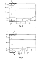
- FIGS. 3 and 4 show two design options for an asymmetrical thyristor.
- the designations in FIGS. 3 and 4 are identical to those in FIG.
- the doping profiles outside the region of the p + emitter again correspond to those according to FIGS. 1b and 2b.
- a cathode metallization 7 and an anode metallization 8 are also attached.
- two different stop layers 4 are provided, or one stop layer with regions of different donor concentration.
- the donor concentration of the stop layer corresponds to the formula (1).
- the donor concentration is increased in the region of the p + emitter.
- the idea according to the invention essentially consists in the case of semiconductor components which block only one polarity, such as diodes, reverse-conducting and asymmetrical thyristors with a pn-n layer sequence, and close the n-region acting as a stop layer according to the formula (1) dope and contour appropriately at the edge.
- this edge contouring is therefore not due to the blocking pn junction, but on the side of the n - n layer sequence that is distant from it.
Landscapes
- Thyristors (AREA)
Applications Claiming Priority (2)
| Application Number | Priority Date | Filing Date | Title |
|---|---|---|---|
| CH654483 | 1983-12-07 | ||
| CH6544/83 | 1983-12-07 |
Publications (3)
| Publication Number | Publication Date |
|---|---|
| EP0144876A2 true EP0144876A2 (fr) | 1985-06-19 |
| EP0144876A3 EP0144876A3 (en) | 1985-07-03 |
| EP0144876B1 EP0144876B1 (fr) | 1988-03-09 |
Family
ID=4311263
Family Applications (1)
| Application Number | Title | Priority Date | Filing Date |
|---|---|---|---|
| EP84114203A Expired EP0144876B1 (fr) | 1983-12-07 | 1984-11-24 | Dispositif à semi-conducteurs |
Country Status (4)
| Country | Link |
|---|---|
| US (1) | US4642669A (fr) |
| EP (1) | EP0144876B1 (fr) |
| JP (1) | JPS60192367A (fr) |
| DE (1) | DE3469830D1 (fr) |
Cited By (5)
| Publication number | Priority date | Publication date | Assignee | Title |
|---|---|---|---|---|
| EP0214485A3 (fr) * | 1985-09-05 | 1988-03-09 | eupec Europäische Gesellschaft für Leistungshalbleiter mbH & Co. KG | Thyristor asymétrique et son procédé de fabrication |
| EP0350670A3 (en) * | 1988-06-20 | 1990-12-05 | Kabushiki Kaisha Meidensha | Semiconductor device with a high breakdown voltage |
| DE4342482A1 (de) * | 1993-12-13 | 1995-06-14 | Siemens Ag | Schnelle Leistungshalbleiterbauelemente mit strukturierter Basis |
| WO2000004597A3 (fr) * | 1998-07-13 | 2000-04-20 | Siemens Ag | Composant a semi-conducteur de puissance a blocage asymetrique |
| WO2000042662A1 (fr) * | 1999-01-12 | 2000-07-20 | eupec Europäische Gesellschaft für Leistungshalbleiter mbH & Co. KG | Composant a semi-conducteur de puissance a bord mesa |
Families Citing this family (9)
| Publication number | Priority date | Publication date | Assignee | Title |
|---|---|---|---|---|
| EP0230278A3 (fr) * | 1986-01-24 | 1989-09-06 | Siemens Aktiengesellschaft | Thyristor avec dispositif d'alimentation intégré d'un circuit défini et procédé pour sa fabrication |
| EP0409010A1 (fr) * | 1989-07-19 | 1991-01-23 | Asea Brown Boveri Ag | Dispositif semi-conducteur de puissance, à extinction |
| JP3044975B2 (ja) * | 1992-12-10 | 2000-05-22 | トヨタ自動車株式会社 | 電気自動車のバッテリ加温装置 |
| US5967795A (en) * | 1995-08-30 | 1999-10-19 | Asea Brown Boveri Ab | SiC semiconductor device comprising a pn junction with a voltage absorbing edge |
| US6271545B1 (en) * | 1997-01-31 | 2001-08-07 | Siemens Aktiengesellschaft | Asymmetrical thyristor with blocking/sweep voltage independent of temperature behavior |
| JP3638873B2 (ja) * | 1998-07-17 | 2005-04-13 | インフィネオン テクノロジース アクチエンゲゼルシャフト | ストップゾーンを有するエミッタ領域を備えたパワー半導体素子 |
| JP4960042B2 (ja) | 2006-08-28 | 2012-06-27 | プライムアースEvエナジー株式会社 | ヒータ付き組電池構造体 |
| JP5105809B2 (ja) | 2006-09-19 | 2012-12-26 | プライムアースEvエナジー株式会社 | ヒータユニット、ヒータ付き電池構造体 |
| JP2012531049A (ja) * | 2009-06-19 | 2012-12-06 | エスエス エスシー アイピー、エルエルシー | 傾斜ドープ領域を有する縦型接合電界効果トランジスターおよびダイオードならびに製造方法 |
Family Cites Families (14)
| Publication number | Priority date | Publication date | Assignee | Title |
|---|---|---|---|---|
| US3370209A (en) * | 1964-08-31 | 1968-02-20 | Gen Electric | Power bulk breakdown semiconductor devices |
| CH426020A (de) * | 1965-09-08 | 1966-12-15 | Bbc Brown Boveri & Cie | Verfahren zur Herstellung des Halbleiterelementes eines stossspannungsfesten Halbleiterventils, sowie ein mit Hilfe dieses Verfahrens hergestelltes Halbleiterelement |
| GB1145392A (en) * | 1967-03-08 | 1969-03-12 | Ass Elect Ind | Improvements in semi-conductor rectifiers |
| US3697829A (en) * | 1968-12-30 | 1972-10-10 | Gen Electric | Semiconductor devices with improved voltage breakdown characteristics |
| CH589942A5 (fr) * | 1975-09-09 | 1977-07-29 | Bbc Brown Boveri & Cie | |
| NL180265C (nl) * | 1976-06-21 | 1987-01-16 | Gen Electric | Halfgeleiderinrichting voor hoge spanning. |
| US4214255A (en) * | 1977-02-07 | 1980-07-22 | Rca Corporation | Gate turn-off triac with dual low conductivity regions contacting central gate region |
| JPS5933272B2 (ja) * | 1978-06-19 | 1984-08-14 | 株式会社日立製作所 | 半導体装置 |
| US4255757A (en) * | 1978-12-05 | 1981-03-10 | International Rectifier Corporation | High reverse voltage semiconductor device with fast recovery time with central depression |
| GB2045000A (en) * | 1979-03-19 | 1980-10-22 | Westinghouse Electric Corp | An asymmetric thyristor |
| DE3068968D1 (en) * | 1979-11-16 | 1984-09-20 | Gen Electric | Asymmetrical field controlled thyristor |
| US4305084A (en) * | 1979-11-16 | 1981-12-08 | General Electric Company | Semiconductor switching device capable of turn-on only at low applied voltages using self pinch-off means |
| DE3017313A1 (de) * | 1980-05-06 | 1981-11-12 | Siemens AG, 1000 Berlin und 8000 München | Thyristor mit hoher blockierspannung und verfahren zu seiner herstellung |
| EP0074133B1 (fr) * | 1981-08-25 | 1987-01-28 | BBC Aktiengesellschaft Brown, Boveri & Cie. | Thyristor |
-
1984
- 1984-11-24 DE DE8484114203T patent/DE3469830D1/de not_active Expired
- 1984-11-24 EP EP84114203A patent/EP0144876B1/fr not_active Expired
- 1984-12-07 US US06/679,359 patent/US4642669A/en not_active Expired - Fee Related
- 1984-12-07 JP JP59257734A patent/JPS60192367A/ja active Pending
Cited By (7)
| Publication number | Priority date | Publication date | Assignee | Title |
|---|---|---|---|---|
| EP0214485A3 (fr) * | 1985-09-05 | 1988-03-09 | eupec Europäische Gesellschaft für Leistungshalbleiter mbH & Co. KG | Thyristor asymétrique et son procédé de fabrication |
| EP0350670A3 (en) * | 1988-06-20 | 1990-12-05 | Kabushiki Kaisha Meidensha | Semiconductor device with a high breakdown voltage |
| DE4342482A1 (de) * | 1993-12-13 | 1995-06-14 | Siemens Ag | Schnelle Leistungshalbleiterbauelemente mit strukturierter Basis |
| WO2000004597A3 (fr) * | 1998-07-13 | 2000-04-20 | Siemens Ag | Composant a semi-conducteur de puissance a blocage asymetrique |
| DE19981343B4 (de) * | 1998-07-13 | 2004-03-18 | Infineon Technologies Ag | Asymmetrisch sperrendes Leistungshalbleiterbauelement |
| WO2000042662A1 (fr) * | 1999-01-12 | 2000-07-20 | eupec Europäische Gesellschaft für Leistungshalbleiter mbH & Co. KG | Composant a semi-conducteur de puissance a bord mesa |
| US6696705B1 (en) | 1999-01-12 | 2004-02-24 | Eupec Europaeische Gesellschaft Fuer Leistungshalbleiter Mbh & Co. Kg | Power semiconductor component having a mesa edge termination |
Also Published As
| Publication number | Publication date |
|---|---|
| EP0144876A3 (en) | 1985-07-03 |
| US4642669A (en) | 1987-02-10 |
| EP0144876B1 (fr) | 1988-03-09 |
| JPS60192367A (ja) | 1985-09-30 |
| DE3469830D1 (en) | 1988-04-14 |
Similar Documents
| Publication | Publication Date | Title |
|---|---|---|
| DE112011103230B4 (de) | Non-Punch-Through-Bipolarleistungshalbleiterbauelement und ein Verfahren zum Herstellen eines derartigen Halbleiterbauelements | |
| DE102009036930B4 (de) | Halbleiterbauelement und Verfahren zur Herstellung eines Halbleiterbauelements | |
| DE102017219159B4 (de) | Halbleitervorrichtung und Fertigungsverfahren dafür | |
| WO2000042662A1 (fr) | Composant a semi-conducteur de puissance a bord mesa | |
| CH638928A5 (de) | Halbleiteranordnung. | |
| DE112021002169T5 (de) | Halbleitervorrichtung | |
| DE102004012884B4 (de) | Leistungs-Halbleiterbauelement in Planartechnik | |
| EP0144876B1 (fr) | Dispositif à semi-conducteurs | |
| CH668505A5 (de) | Halbleiterbauelement. | |
| CH633907A5 (de) | Leistungshalbleiterbauelement mit zonen-guard-ringen. | |
| EP1131852B1 (fr) | Composant semi-conducteur dote de structures de blindage dielectriques ou semi-isolantes | |
| DE10235198B4 (de) | Leistungs-Halbleitergleichrichter mit ringförmigen Gräben | |
| DE102021103703A1 (de) | Hochvolt-Randabschluss-Struktur für Leistungshalbleiterbauelemente und Verfahren zum Herstellen derselben | |
| DE19753673A1 (de) | Schottky-Diode | |
| EP0014435B1 (fr) | Thyristor commandé par transistor à effet de champ | |
| DE2500775A1 (de) | Hochspannungsfestes halbleiterbauelement | |
| EP0074133A2 (fr) | Thyristor | |
| DE3832750A1 (de) | Leistungshalbleiterbauelement | |
| EP0303046A1 (fr) | Thyristor à commande d'extinction | |
| EP0651445A2 (fr) | Thyristor bloquable | |
| WO1997011495A1 (fr) | Systeme a jonction pn presentant un moyen visant a reduire le risque de rupture de la jonction pn | |
| DE102020121768B4 (de) | Mehrfach-Trench-Schottky-Diode | |
| DE2356674C2 (de) | Halbleiterbauelement mit einem scheibenförmigen Halbleiterkörper | |
| DE102013218494A1 (de) | Halbleiterbauelement mit einer Passivierungsschicht und Herstellungsverfahren | |
| DE19981343B4 (de) | Asymmetrisch sperrendes Leistungshalbleiterbauelement |
Legal Events
| Date | Code | Title | Description |
|---|---|---|---|
| PUAI | Public reference made under article 153(3) epc to a published international application that has entered the european phase |
Free format text: ORIGINAL CODE: 0009012 |
|
| PUAL | Search report despatched |
Free format text: ORIGINAL CODE: 0009013 |
|
| AK | Designated contracting states |
Designated state(s): CH DE FR GB IT LI NL SE |
|
| AK | Designated contracting states |
Designated state(s): CH DE FR GB IT LI NL SE |
|
| 17P | Request for examination filed |
Effective date: 19851028 |
|
| 17Q | First examination report despatched |
Effective date: 19860605 |
|
| RAP1 | Party data changed (applicant data changed or rights of an application transferred) |
Owner name: BBC BROWN BOVERI AG |
|
| GRAA | (expected) grant |
Free format text: ORIGINAL CODE: 0009210 |
|
| AK | Designated contracting states |
Kind code of ref document: B1 Designated state(s): CH DE FR GB IT LI NL SE |
|
| PG25 | Lapsed in a contracting state [announced via postgrant information from national office to epo] |
Ref country code: NL Effective date: 19880309 |
|
| REF | Corresponds to: |
Ref document number: 3469830 Country of ref document: DE Date of ref document: 19880414 |
|
| ITF | It: translation for a ep patent filed | ||
| GBT | Gb: translation of ep patent filed (gb section 77(6)(a)/1977) | ||
| ET | Fr: translation filed | ||
| NLV1 | Nl: lapsed or annulled due to failure to fulfill the requirements of art. 29p and 29m of the patents act | ||
| PLBE | No opposition filed within time limit |
Free format text: ORIGINAL CODE: 0009261 |
|
| STAA | Information on the status of an ep patent application or granted ep patent |
Free format text: STATUS: NO OPPOSITION FILED WITHIN TIME LIMIT |
|
| PGFP | Annual fee paid to national office [announced via postgrant information from national office to epo] |
Ref country code: DE Payment date: 19890128 Year of fee payment: 5 |
|
| PGFP | Annual fee paid to national office [announced via postgrant information from national office to epo] |
Ref country code: CH Payment date: 19890221 Year of fee payment: 5 |
|
| 26N | No opposition filed | ||
| PGFP | Annual fee paid to national office [announced via postgrant information from national office to epo] |
Ref country code: FR Payment date: 19891016 Year of fee payment: 6 |
|
| PGFP | Annual fee paid to national office [announced via postgrant information from national office to epo] |
Ref country code: SE Payment date: 19891023 Year of fee payment: 6 |
|
| PGFP | Annual fee paid to national office [announced via postgrant information from national office to epo] |
Ref country code: GB Payment date: 19891031 Year of fee payment: 6 |
|
| ITTA | It: last paid annual fee | ||
| PG25 | Lapsed in a contracting state [announced via postgrant information from national office to epo] |
Ref country code: LI Effective date: 19891130 Ref country code: CH Effective date: 19891130 |
|
| REG | Reference to a national code |
Ref country code: CH Ref legal event code: PL |
|
| PG25 | Lapsed in a contracting state [announced via postgrant information from national office to epo] |
Ref country code: DE Effective date: 19900801 |
|
| PG25 | Lapsed in a contracting state [announced via postgrant information from national office to epo] |
Ref country code: GB Effective date: 19901124 |
|
| PG25 | Lapsed in a contracting state [announced via postgrant information from national office to epo] |
Ref country code: SE Effective date: 19901125 |
|
| GBPC | Gb: european patent ceased through non-payment of renewal fee | ||
| PG25 | Lapsed in a contracting state [announced via postgrant information from national office to epo] |
Ref country code: FR Effective date: 19910731 |
|
| REG | Reference to a national code |
Ref country code: FR Ref legal event code: ST |
|
| EUG | Se: european patent has lapsed |
Ref document number: 84114203.7 Effective date: 19910705 |