EP0144900A2 - Dispositif de mémoire électriquement programmable et procédé pour fabriquer ce dispositif - Google Patents
Dispositif de mémoire électriquement programmable et procédé pour fabriquer ce dispositif Download PDFInfo
- Publication number
- EP0144900A2 EP0144900A2 EP84114348A EP84114348A EP0144900A2 EP 0144900 A2 EP0144900 A2 EP 0144900A2 EP 84114348 A EP84114348 A EP 84114348A EP 84114348 A EP84114348 A EP 84114348A EP 0144900 A2 EP0144900 A2 EP 0144900A2
- Authority
- EP
- European Patent Office
- Prior art keywords
- layer
- insulating material
- floating gate
- angstroms
- silicon
- Prior art date
- Legal status (The legal status is an assumption and is not a legal conclusion. Google has not performed a legal analysis and makes no representation as to the accuracy of the status listed.)
- Granted
Links
- 238000000034 method Methods 0.000 title claims abstract description 33
- 238000007667 floating Methods 0.000 claims abstract description 53
- 229910021420 polycrystalline silicon Inorganic materials 0.000 claims abstract description 35
- 229910052698 phosphorus Inorganic materials 0.000 claims abstract description 17
- 239000011574 phosphorus Substances 0.000 claims abstract description 17
- OAICVXFJPJFONN-UHFFFAOYSA-N Phosphorus Chemical compound [P] OAICVXFJPJFONN-UHFFFAOYSA-N 0.000 claims abstract description 15
- 238000007254 oxidation reaction Methods 0.000 claims abstract description 11
- 230000003647 oxidation Effects 0.000 claims abstract description 10
- 238000004518 low pressure chemical vapour deposition Methods 0.000 claims abstract description 9
- 239000002019 doping agent Substances 0.000 claims abstract 7
- VYPSYNLAJGMNEJ-UHFFFAOYSA-N Silicium dioxide Chemical compound O=[Si]=O VYPSYNLAJGMNEJ-UHFFFAOYSA-N 0.000 claims description 90
- 239000000377 silicon dioxide Substances 0.000 claims description 37
- 239000011810 insulating material Substances 0.000 claims description 31
- 229910052681 coesite Inorganic materials 0.000 claims description 28
- 229910052906 cristobalite Inorganic materials 0.000 claims description 28
- 229910052682 stishovite Inorganic materials 0.000 claims description 28
- 229910052905 tridymite Inorganic materials 0.000 claims description 28
- 239000000463 material Substances 0.000 claims description 27
- 235000012239 silicon dioxide Nutrition 0.000 claims description 19
- 229910052581 Si3N4 Inorganic materials 0.000 claims description 14
- 238000000151 deposition Methods 0.000 claims description 11
- XUIMIQQOPSSXEZ-UHFFFAOYSA-N Silicon Chemical compound [Si] XUIMIQQOPSSXEZ-UHFFFAOYSA-N 0.000 claims description 10
- 229910052710 silicon Inorganic materials 0.000 claims description 9
- 239000010703 silicon Substances 0.000 claims description 9
- 239000002253 acid Substances 0.000 claims description 5
- 238000005468 ion implantation Methods 0.000 claims description 4
- 238000004519 manufacturing process Methods 0.000 claims description 4
- 230000001698 pyrogenic effect Effects 0.000 claims description 4
- 239000004020 conductor Substances 0.000 claims 1
- 230000008878 coupling Effects 0.000 abstract description 8
- 238000010168 coupling process Methods 0.000 abstract description 8
- 238000005859 coupling reaction Methods 0.000 abstract description 8
- 229920005591 polysilicon Polymers 0.000 abstract description 5
- 239000003989 dielectric material Substances 0.000 abstract description 4
- 230000015556 catabolic process Effects 0.000 abstract description 3
- 238000009792 diffusion process Methods 0.000 abstract description 2
- 230000000694 effects Effects 0.000 abstract 1
- 238000002955 isolation Methods 0.000 abstract 1
- HQVNEWCFYHHQES-UHFFFAOYSA-N silicon nitride Chemical compound N12[Si]34N5[Si]62N3[Si]51N64 HQVNEWCFYHHQES-UHFFFAOYSA-N 0.000 description 11
- 150000004767 nitrides Chemical class 0.000 description 5
- BLRPTPMANUNPDV-UHFFFAOYSA-N Silane Chemical compound [SiH4] BLRPTPMANUNPDV-UHFFFAOYSA-N 0.000 description 4
- 230000005684 electric field Effects 0.000 description 4
- 239000000758 substrate Substances 0.000 description 4
- -1 i.e. Substances 0.000 description 3
- QAOWNCQODCNURD-UHFFFAOYSA-N Sulfuric acid Chemical compound OS(O)(=O)=O QAOWNCQODCNURD-UHFFFAOYSA-N 0.000 description 2
- 238000006243 chemical reaction Methods 0.000 description 2
- 229910021419 crystalline silicon Inorganic materials 0.000 description 2
- 230000009977 dual effect Effects 0.000 description 2
- 150000002500 ions Chemical class 0.000 description 2
- XHXFXVLFKHQFAL-UHFFFAOYSA-N phosphoryl trichloride Chemical compound ClP(Cl)(Cl)=O XHXFXVLFKHQFAL-UHFFFAOYSA-N 0.000 description 2
- XLYOFNOQVPJJNP-UHFFFAOYSA-N water Substances O XLYOFNOQVPJJNP-UHFFFAOYSA-N 0.000 description 2
- 230000005689 Fowler Nordheim tunneling Effects 0.000 description 1
- 229910019213 POCl3 Inorganic materials 0.000 description 1
- 229910003818 SiH2Cl2 Inorganic materials 0.000 description 1
- 230000015572 biosynthetic process Effects 0.000 description 1
- 238000011960 computer-aided design Methods 0.000 description 1
- 238000011109 contamination Methods 0.000 description 1
- 238000007599 discharging Methods 0.000 description 1
- 239000012153 distilled water Substances 0.000 description 1
- 238000005516 engineering process Methods 0.000 description 1
- 238000010943 off-gassing Methods 0.000 description 1
- 238000009877 rendering Methods 0.000 description 1
- 239000000126 substance Substances 0.000 description 1
Images

Classifications
-
- H—ELECTRICITY
- H10—SEMICONDUCTOR DEVICES; ELECTRIC SOLID-STATE DEVICES NOT OTHERWISE PROVIDED FOR
- H10D—INORGANIC ELECTRIC SEMICONDUCTOR DEVICES
- H10D30/00—Field-effect transistors [FET]
- H10D30/60—Insulated-gate field-effect transistors [IGFET]
- H10D30/69—IGFETs having charge trapping gate insulators, e.g. MNOS transistors
-
- H—ELECTRICITY
- H10—SEMICONDUCTOR DEVICES; ELECTRIC SOLID-STATE DEVICES NOT OTHERWISE PROVIDED FOR
- H10D—INORGANIC ELECTRIC SEMICONDUCTOR DEVICES
- H10D30/00—Field-effect transistors [FET]
- H10D30/60—Insulated-gate field-effect transistors [IGFET]
- H10D30/68—Floating-gate IGFETs
- H10D30/681—Floating-gate IGFETs having only two programming levels
- H10D30/683—Floating-gate IGFETs having only two programming levels programmed by tunnelling of carriers, e.g. Fowler-Nordheim tunnelling
-
- H—ELECTRICITY
- H10—SEMICONDUCTOR DEVICES; ELECTRIC SOLID-STATE DEVICES NOT OTHERWISE PROVIDED FOR
- H10D—INORGANIC ELECTRIC SEMICONDUCTOR DEVICES
- H10D64/00—Electrodes of devices having potential barriers
- H10D64/01—Manufacture or treatment
- H10D64/031—Manufacture or treatment of data-storage electrodes
- H10D64/035—Manufacture or treatment of data-storage electrodes comprising conductor-insulator-conductor-insulator-semiconductor structures
Definitions
- the present invention relates to an electrically programmable device and a method for making the same.
- the electrically programmable memory device can be of the type that is commonly called Electrically Programmable Read-Only Memory (EPROM) or Electrically Erasable Programmable Read-Only Memory (EEPROM). More particularly, the present invention relates to the manufacture of ultra high coupling interpoly dielectrics suitable for programming EEPROM and EPROM devices at faster speeds and lower voltages than heretofore achieved. A higher interpoly dielectric breakdown capability and higher interpoly capacitance is required for VLSI technology due to the preferred smaller die size in high circuit density package. The invention involves the development of thinner and stronger interpoly dielectrics.
- an EPROM or an EEPROM and methods for making the same are well known in the art.
- an EPROM or an EEPROM is characterized by a "floating gate” and a electrical connection termed “control gate”, both of which are fabricated out of polycrystalline silicon doped with an appropriate doping material to render the polycrystalline conductive.' A typical doping material is phosphorus.
- the floating gate and the control gate are separated by a layer of insulating material, typically silicon dioxide (Si02).
- Si02 silicon dioxide
- the principle upon which the EPROM or EEPROM device operates is that charges are stored on the "floating gate” in a capacitive manner.
- the dielectric of the layer of silicon dioxide between the floating gate and the control gate is important.
- the floating gate is formed by reacting S i H4 in a low pressure chemical vapor deposition chamber and then doped with POC1 3 .
- a layer of silicon dioxide is then deposited or thermally grown on the doped polycrystalline layer of silicon.
- the layer of silicon dioxide is typically approximately 750 angstroms. Generally, a high oxidation temperature (greater than 1050°C) and heavier phosphorus doping are required to achieve better interpoly quality on breakdown capability.
- oxidation at high temperature on heavily-doped polysilicon involves several drawbacks, such as: (1) outgassing during interpoly oxidation which causes autodoping on wafer. (2) oxidation enhanced diffusion of phosphorus from the floating gate to the tunnel oxide, which, forms a trapping center in the oxide. The phosphorus induced trap collapses the threshold window of EEPROM cell at 10 4 cycles. (See: R.B. Marcus et al., J. Electrochem. Soc., p. 1282, June, 1982; K. Saraswat et al., Computer-Aided Design of Integrated Circuit Fabrication Process for VLSI Device, p. 244-290, July, 1981.) Finally, the second layer of doped polycrystalline silicon is then formed on top of the insulating layer of SiO 2 .
- the typical write or erase voltage i.e., the voltage which is needed to place charges on or to remove charges off the floating gate has been high, i.e., in excess of 20 volts, which places the shrinkage limits for gate oxide thickness, junction depth and die size.
- Silicon nitride (Si 3 N 4 ) has also been used as an insulating layer of dual dielectric (thermal oxide with silicon nitride on it) between the floating gate and the control gate connection. Silicon nitride has the property that it is more dense than silicon dioxide and, therefore, affords higher capacitive coupling between the floating gate and the control gate.
- a typical dual dielectric between the floating gate and the control gate is composed of 500 angstroms oxide and 400 angstroms nitride.
- the write and erase voltage is still relatively high, in excess of 20 volts. This is due to the problem of asperity or roughness in the surface of the floating gate. Asperity in the floating gate causes points of electrical field enhancement. Thus, a large amount of insulating material must be interposed between the floating gate and the -control gate. This, however, in turn, requires that a large voltage be used.
- an electrically programmable memory device in which the floating gate is first formed by depositing a layer of polycrystalline silicon. Subsequently, a layer of silicon dioxide of approximately 200 angstroms is thermally formed over the polycrystalline silicon. The layer of polycrystalline silicon is then doped by ion implantation technique in which ions are implanted through the insulating layer of silicon dioxide into the layer of polycrystallihe silicon to dope it to form the floating gate. A LPCVD silicon nitride (approximately 200 angstroms) is then deposited on the layer of silicon dioxide. Finally, a pyrogenic oxidation (H Z/ 0 2 ) is performed to reduce the nitride pinhole and nitride/oxide interface state.
- H Z/ 0 2 pyrogenic oxidation
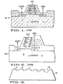
- the EPROM 10 comprises a substrate 12, which is typically a single crystalline silicon of the P type having a source 14 and a drain 16 fabricated therein.
- a first layer 18 of insulating material, typically SiO 2 is grown on the silicon substrate 12.
- the first layer 18 of SiO 2 is thermally grown at approximately 1,000 degree centigrade, using HC1 and 0 2 .
- On the first layer 18 of Si0 2 is deposited the first layer 20 of polycrystalline silicon.
- the first layer 20 of polycrystalline 20 is deposited by low pressure chemical vapor deposition techniques. In a reaction chamber, SiH 4 is introduced and is reacted at approximately between 620-670 degrees centigrade, depositing the layer 20 of polycrystalline silicon.
- the first layer 20 of polycrystalline silicon is then doped by phosphorus, rendering it conductive to form the floating gate.
- Phosphorus is introduced into the reaction chamber in the form of POCl 3 at 950 degrees centigrade.
- a second layer 22 of insulating material, i.e., SiO 2 is thermally grown on the floating gate 20.
- the second layer 22 of Si0 2 is typically on the order of 750 to 1000 angstroms.
- a second layer 24 of polycrystalline is deposited on the second layer 22 of SiO 2 .
- the second layer 24 of polycrystalline silicon is doped to form the connection for the control gate of the EPROM 10.
- EEPROM 110 of the prior art there is shown an EEPROM 110 of the prior art.
- the EEPROM 110 of the prior art is identical to the EPROM 10 of the prior art, shown in Fig. 1, except for the tunnel oxide 15 region between the drain 16 and the floating gate 20.
- the tunnel oxide region is typically approximately 100 angstroms thick. This narrow, thin tunnel oxide region 15 permits electrons to tunnel to or from the drain 16 during the erase or write cycle.
- the fabrication of the first layer 18 and second layer 22 of SiO 2 and the formation of the floating gate 20 and of the control gate 24 is similar to that described for the EPROM 10 of Fig. 1.
- the first layer 18 of Si0 2 is thermally grown on the single crystalline substrate 12 in the same manner as that for the EPROM 10 or the EEPROM 110 of the prior art.
- the floating gate 20, however, is formed by depositing a layer of polycrystalline silicon on the first layer 18 of SiO 2 .
- the layer 20 of polycrystalline silicon is deposited by low pressure chemical vapor deposition technique in which S i H4 is introduced and is reacted at approximately between 620-670 centigrade.
- the second layer 22 of SiO 2 is then thermally grown on the first layer 20 of undoped polycrystalline silicon.
- the second layer 22 of Si0 2 is approximately 250 angstroms thick.
- Phosphorus ions are then implanted in the first layer 20 of polycrystalline silicon through the second layer 22 of Si0 2 .
- the phosphorus ions are accelerated at 70-120 KEV to impinge the second layer 22 of SiO 2 , to pass therethrough and to be deposited in the first layer 20 of polycrystalline silicon.
- SiO 2 can then be further deposited on top of the second layer 22 of SiO 2 to increase the total thickness to approximately 400-500 angstroms.
- the second layer 24 of polycrystalline silicon is then deposited on the second layer 22 of silicon dioxide in the same manner as the prior art.
- the second layer 24 of polycrystalline can then be doped to be conductive to form the control gate.
- FIG. 3 there is shown a section of the floating gate 20 of the EPROM 10 or EEPROM 110 of the prior art (shown in solid line) and a section of the floating gate 120 of the EPROM or EEPROM made by the method of the present invention (shown in dotted lines). This is a greatly enlarged view, as typically the dimension of the floating gate is less than one micron in size.
- the floating gate 20 of the prior art shows a number of bumps (designated as A, B, C, etc.).
- the asperity in the floating gate 20 is attributable to the chemical phosphorus doping of the polycrystalline silicon.
- These bumps in the floating gate 20 form electrical field enhancement points.
- the surface is relatively smooth.
- the doping material is not chemically introduced and does not deform the surface of the floating gate 120.
- the second layer 22 of silicon dioxide can be on the order of 400-500 angstroms. This increases the capacitive coupling. Thus, the operating voltage for the write and erase cycles can be much lower.
- the charging and discharging of the floating gate is accomplished by Fowler-Nordheim tunneling of electron across the tunnel oxide.
- the tunnel current where E is the electric field across the tunnel oxide, ⁇ and ⁇ are constants, electrical field where V is the voltage drop across the tunnel oxide and t is the tunnel oxide thickness.
- V can be calculated from the capacitive equivalent voltage divider circuit.
- the coupling ratio is where C total is the sum of interpoly capacitance (Cpp), gate oxide capacitance and tunnel oxide capacitance. Higher interpoly capacitance results in higher coupling ratio, which, results either in the reduction of charging state applied programming voltage or in shorter charging state programming time.
- the EPROM 210 comprises a single crystalline silicon substrate 212, having a source 214 and a drain 216.
- a first layer 218 of Si0 2 is on the body 212.
- a first layer of undoped polycrystalline silicon 220 is on the first layer 218 of silicon dioxide.
- the first layer 220 is deposited by low pressure chemical vapor deposition technique of SiH 4 at 620°C.
- the layer 220 is approximately between 3000-4500 angstroms thick.
- a second layer 222 of silicon dioxide is on the first layer 220 of polycrystalline silicon.
- the second layer 222 is substantially between 200-250 angstroms.
- the second layer 220 is formed by thermal oxidation of dry 0 2 at approximately 1000°C.
- the first layer 220 of polycrystalline silicon is doped with phosphorus that has been ion implanted through the second layer of 222 of silicon dioxide.
- P 31 is implanted at 1-5 x 10 15 /cm 2 at 70-120 KEV.
- the second layer 222 of silicon dioxide is bathed in sulfuric acid at 150°C for about 10 minutes.
- the second layer 222 is dipped in a dilute HF acid for about 5 seconds to remove contamination due to the ion implantation.
- the HF acid removes approximately 25 angstroms of Si0 2 .
- the dilute HF acid comprises ten parts of distill water to one part of HF acid.
- the second layer 222 is then rinsed in distilled water and dried.
- a third layer 224 of insulating material is deposited on the second layer 222 of silicon dioxide.
- the third layer 224 comprises silicon nitride (Si 3 N 4 ) and is deposited by low pressure chemical vapor deposition technique. NH 3 and SiH 2 Cl 2 are reacted at approximately 770°C.
- the third layer 224 is approximately 250 angstroms.
- a pyrogenic oxidation (H 2 /0 2 ) cycle is then performed to reduce the nitride pinhole and nitride/oxide interface state. The pyrogenic oxidation step is accomplished by reacting H 2 and 0 2 at 900°C for about 2 hours.
- the third layer 226 of SiO 2 which is between approximately 30-50 angstroms.
- the second layer 228 of polycrystalline silicon is then deposited on the third layer 226 of SiO 2 .
- the second layer 228 of polycrystalline silicon is then doped to form the control gate.
- EEPROM 310 of the present invention is identical to the EPROM 210 shown in Fig. 4, except with the addition of a tunnel oxide region 315.
- the first, second, and third layers of insulating material comprising the two layers of Si0 2 and one layer of Si 3 N 4
- the two layers of polycrystalline silicon are identical to the similar structures for the EPROM 210 and are made in the same manner.
- the first layer of Si0 2 is approximately 750 angstroms thick over the thick gate region and is approximately 100 angstroms thick in the tunnel oxide region.
Landscapes
- Non-Volatile Memory (AREA)
- Semiconductor Memories (AREA)
Applications Claiming Priority (2)
| Application Number | Priority Date | Filing Date | Title |
|---|---|---|---|
| US55602883A | 1983-11-28 | 1983-11-28 | |
| US556028 | 1983-11-28 |
Publications (3)
| Publication Number | Publication Date |
|---|---|
| EP0144900A2 true EP0144900A2 (fr) | 1985-06-19 |
| EP0144900A3 EP0144900A3 (en) | 1986-10-08 |
| EP0144900B1 EP0144900B1 (fr) | 1990-06-13 |
Family
ID=24219586
Family Applications (1)
| Application Number | Title | Priority Date | Filing Date |
|---|---|---|---|
| EP84114348A Expired - Lifetime EP0144900B1 (fr) | 1983-11-28 | 1984-11-27 | Dispositif de mémoire électriquement programmable et procédé pour fabriquer ce dispositif |
Country Status (3)
| Country | Link |
|---|---|
| EP (1) | EP0144900B1 (fr) |
| JP (1) | JPS60134478A (fr) |
| DE (1) | DE3482530D1 (fr) |
Cited By (15)
| Publication number | Priority date | Publication date | Assignee | Title |
|---|---|---|---|---|
| EP0187278A3 (en) * | 1984-12-07 | 1986-12-30 | Kabushiki Kaisha Toshiba | Semiconductor device and method for manufacturing the same |
| EP0282022A3 (fr) * | 1987-03-13 | 1989-05-17 | Kabushiki Kaisha Toshiba | Dispositif de mémoire à semi-conducteur |
| EP0326877A3 (en) * | 1988-02-05 | 1990-06-27 | Texas Instruments Incorporated | Electrically-erasable, electrically-programmable read-only memory cell |
| US5012307A (en) * | 1988-07-15 | 1991-04-30 | Texas Instruments Incorporated | Electrically-erasable, electrically-programmable read-only memory |
| US5017980A (en) * | 1988-07-15 | 1991-05-21 | Texas Instruments Incorporated | Electrically-erasable, electrically-programmable read-only memory cell |
| US5057446A (en) * | 1990-08-06 | 1991-10-15 | Texas Instruments Incorporated | Method of making an EEPROM with improved capacitive coupling between control gate and floating gate |
| US5063171A (en) * | 1990-04-06 | 1991-11-05 | Texas Instruments Incorporated | Method of making a diffusionless virtual drain and source conductor/oxide semiconductor field effect transistor |
| US5150179A (en) * | 1990-07-05 | 1992-09-22 | Texas Instruments Incorporated | Diffusionless source/drain conductor electrically-erasable, electrically-programmable read-only memory and method for making and using the same |
| US5156991A (en) * | 1988-02-05 | 1992-10-20 | Texas Instruments Incorporated | Fabricating an electrically-erasable, electrically-programmable read-only memory having a tunnel window insulator and thick oxide isolation between wordlines |
| US5218568A (en) * | 1991-12-17 | 1993-06-08 | Texas Instruments Incorporated | Electrically-erasable, electrically-programmable read-only memory cell, an array of such cells and methods for making and using the same |
| US5225700A (en) * | 1991-06-28 | 1993-07-06 | Texas Instruments Incorporated | Circuit and method for forming a non-volatile memory cell |
| US5262846A (en) * | 1988-11-14 | 1993-11-16 | Texas Instruments Incorporated | Contact-free floating-gate memory array with silicided buried bitlines and with single-step-defined floating gates |
| US5273926A (en) * | 1991-06-27 | 1993-12-28 | Texas Instruments Incorporated | Method of making flash EEPROM or merged FAMOS cell without alignment sensitivity |
| US6501123B2 (en) * | 2001-03-06 | 2002-12-31 | Macronix International Co., Ltd. | High gate coupling non-volatile memory structure |
| US7529368B2 (en) | 2003-04-18 | 2009-05-05 | Via Technologies, Inc. | Apparatus and method for performing transparent output feedback mode cryptographic functions |
Families Citing this family (2)
| Publication number | Priority date | Publication date | Assignee | Title |
|---|---|---|---|---|
| JP2633571B2 (ja) * | 1987-07-30 | 1997-07-23 | 株式会社東芝 | 紫外線消去型不揮発性半導体装置 |
| JP4874729B2 (ja) * | 2006-07-14 | 2012-02-15 | Hoya株式会社 | 撮影装置用清掃器具 |
Family Cites Families (7)
| Publication number | Priority date | Publication date | Assignee | Title |
|---|---|---|---|---|
| US3945856A (en) * | 1974-07-15 | 1976-03-23 | Ibm Corporation | Method of ion implantation through an electrically insulative material |
| US3996657A (en) * | 1974-12-30 | 1976-12-14 | Intel Corporation | Double polycrystalline silicon gate memory device |
| JPS5389686A (en) * | 1977-01-18 | 1978-08-07 | Toshiba Corp | Production of semiconductor memory element |
| JPS5841659B2 (ja) * | 1977-08-30 | 1983-09-13 | 株式会社東芝 | 絶縁膜の形成方法 |
| US4203158A (en) * | 1978-02-24 | 1980-05-13 | Intel Corporation | Electrically programmable and erasable MOS floating gate memory device employing tunneling and method of fabricating same |
| US4355455A (en) * | 1979-07-19 | 1982-10-26 | National Semiconductor Corporation | Method of manufacture for self-aligned floating gate memory cell |
| FR2468185A1 (fr) * | 1980-10-17 | 1981-04-30 | Intel Corp | Procede de fabrication d'une matrice de memoire electriquement programmable a haute densite |
-
1984
- 1984-11-19 JP JP59244324A patent/JPS60134478A/ja active Granted
- 1984-11-27 DE DE8484114348T patent/DE3482530D1/de not_active Expired - Lifetime
- 1984-11-27 EP EP84114348A patent/EP0144900B1/fr not_active Expired - Lifetime
Cited By (18)
| Publication number | Priority date | Publication date | Assignee | Title |
|---|---|---|---|---|
| US4720323A (en) * | 1984-12-07 | 1988-01-19 | Kabushiki Kaisha Toshiba | Method for manufacturing a semiconductor device |
| US4768080A (en) * | 1984-12-07 | 1988-08-30 | Kabushiki Kaisha Toshiba | Semiconductor device having floating and control gates |
| EP0187278A3 (en) * | 1984-12-07 | 1986-12-30 | Kabushiki Kaisha Toshiba | Semiconductor device and method for manufacturing the same |
| EP0282022A3 (fr) * | 1987-03-13 | 1989-05-17 | Kabushiki Kaisha Toshiba | Dispositif de mémoire à semi-conducteur |
| US4996572A (en) * | 1987-03-13 | 1991-02-26 | Kabushiki Kaisha Toshiba | Semiconductor memory device |
| EP0326877A3 (en) * | 1988-02-05 | 1990-06-27 | Texas Instruments Incorporated | Electrically-erasable, electrically-programmable read-only memory cell |
| US5156991A (en) * | 1988-02-05 | 1992-10-20 | Texas Instruments Incorporated | Fabricating an electrically-erasable, electrically-programmable read-only memory having a tunnel window insulator and thick oxide isolation between wordlines |
| US5012307A (en) * | 1988-07-15 | 1991-04-30 | Texas Instruments Incorporated | Electrically-erasable, electrically-programmable read-only memory |
| US5017980A (en) * | 1988-07-15 | 1991-05-21 | Texas Instruments Incorporated | Electrically-erasable, electrically-programmable read-only memory cell |
| US5262846A (en) * | 1988-11-14 | 1993-11-16 | Texas Instruments Incorporated | Contact-free floating-gate memory array with silicided buried bitlines and with single-step-defined floating gates |
| US5063171A (en) * | 1990-04-06 | 1991-11-05 | Texas Instruments Incorporated | Method of making a diffusionless virtual drain and source conductor/oxide semiconductor field effect transistor |
| US5150179A (en) * | 1990-07-05 | 1992-09-22 | Texas Instruments Incorporated | Diffusionless source/drain conductor electrically-erasable, electrically-programmable read-only memory and method for making and using the same |
| US5057446A (en) * | 1990-08-06 | 1991-10-15 | Texas Instruments Incorporated | Method of making an EEPROM with improved capacitive coupling between control gate and floating gate |
| US5273926A (en) * | 1991-06-27 | 1993-12-28 | Texas Instruments Incorporated | Method of making flash EEPROM or merged FAMOS cell without alignment sensitivity |
| US5225700A (en) * | 1991-06-28 | 1993-07-06 | Texas Instruments Incorporated | Circuit and method for forming a non-volatile memory cell |
| US5218568A (en) * | 1991-12-17 | 1993-06-08 | Texas Instruments Incorporated | Electrically-erasable, electrically-programmable read-only memory cell, an array of such cells and methods for making and using the same |
| US6501123B2 (en) * | 2001-03-06 | 2002-12-31 | Macronix International Co., Ltd. | High gate coupling non-volatile memory structure |
| US7529368B2 (en) | 2003-04-18 | 2009-05-05 | Via Technologies, Inc. | Apparatus and method for performing transparent output feedback mode cryptographic functions |
Also Published As
| Publication number | Publication date |
|---|---|
| EP0144900A3 (en) | 1986-10-08 |
| JPS60134478A (ja) | 1985-07-17 |
| EP0144900B1 (fr) | 1990-06-13 |
| JPH0574947B2 (fr) | 1993-10-19 |
| DE3482530D1 (de) | 1990-07-19 |
Similar Documents
| Publication | Publication Date | Title |
|---|---|---|
| US4769340A (en) | Method for making electrically programmable memory device by doping the floating gate by implant | |
| EP0144900A2 (fr) | Dispositif de mémoire électriquement programmable et procédé pour fabriquer ce dispositif | |
| KR0179163B1 (ko) | 비휘발성 메모리 셀 및 그 제조방법 | |
| US4833514A (en) | Planar FAMOS transistor with sealed floating gate and DCS+N2 O oxide | |
| US6069041A (en) | Process for manufacturing non-volatile semiconductor memory device by introducing nitrogen atoms | |
| US5837583A (en) | Method of forming separated floating gate for EEPROM application | |
| US5427970A (en) | Method of making flash memory with high coupling ratio | |
| US7544566B2 (en) | Method for manufacturing a non-volatile electrically alterable memory cell that stores multiple data | |
| US6017795A (en) | Method of fabricating buried source to shrink cell dimension and increase coupling ratio in split-gate flash | |
| US5352619A (en) | Method for improving erase characteristics and coupling ratios of buried bit line flash EPROM devices | |
| US6927134B2 (en) | Method of forming a trench transistor having a superior gate dielectric | |
| US20020109181A1 (en) | Method to increase coupling ratio of source to floating gate in split-gate flash | |
| US5913120A (en) | Process for fabricating integrated devices including nonvolatile memories and transistors with tunnel oxide protection | |
| US6261903B1 (en) | Floating gate method and device | |
| JPH04215481A (ja) | 三次元無接点不揮発性メモリセル及びその製造方法 | |
| USRE31083E (en) | Non-volatile memory devices fabricated from graded or stepped energy band gap insulator MIM or MIS structure | |
| US5016068A (en) | Vertical floating-gate transistor | |
| US5620913A (en) | Method of making a flash memory cell | |
| KR100426487B1 (ko) | 플래쉬 메모리 소자의 플로팅 게이트 형성 방법 | |
| EP0195902B1 (fr) | Structure à double injection d'électrons et procédé utilisant une barrière automatique contre l'oxydation | |
| EP0296418B1 (fr) | Décomposition de silicium amorphe pour la formation des couches diélectriques intercalées pour des dispositifs semi-conducteurs à mémoire | |
| US6326268B1 (en) | Method of fabricating a MONOS flash cell using shallow trench isolation | |
| US4735919A (en) | Method of making a floating gate memory cell | |
| US5981339A (en) | Narrower erase distribution for flash memory by smaller poly grain size | |
| US11640972B2 (en) | Process for fabricating a high-voltage capacitive element, and corresponding integrated circuit |
Legal Events
| Date | Code | Title | Description |
|---|---|---|---|
| PUAI | Public reference made under article 153(3) epc to a published international application that has entered the european phase |
Free format text: ORIGINAL CODE: 0009012 |
|
| 17P | Request for examination filed |
Effective date: 19841127 |
|
| AK | Designated contracting states |
Designated state(s): BE DE FR GB IT NL |
|
| PUAL | Search report despatched |
Free format text: ORIGINAL CODE: 0009013 |
|
| AK | Designated contracting states |
Kind code of ref document: A3 Designated state(s): BE DE FR GB IT NL |
|
| 17Q | First examination report despatched |
Effective date: 19880801 |
|
| GRAA | (expected) grant |
Free format text: ORIGINAL CODE: 0009210 |
|
| AK | Designated contracting states |
Kind code of ref document: B1 Designated state(s): BE DE FR GB IT NL |
|
| PG25 | Lapsed in a contracting state [announced via postgrant information from national office to epo] |
Ref country code: NL Effective date: 19900613 Ref country code: BE Effective date: 19900613 |
|
| ITF | It: translation for a ep patent filed | ||
| REF | Corresponds to: |
Ref document number: 3482530 Country of ref document: DE Date of ref document: 19900719 |
|
| ET | Fr: translation filed | ||
| NLV1 | Nl: lapsed or annulled due to failure to fulfill the requirements of art. 29p and 29m of the patents act | ||
| PG25 | Lapsed in a contracting state [announced via postgrant information from national office to epo] |
Ref country code: GB Effective date: 19901127 |
|
| PLBE | No opposition filed within time limit |
Free format text: ORIGINAL CODE: 0009261 |
|
| STAA | Information on the status of an ep patent application or granted ep patent |
Free format text: STATUS: NO OPPOSITION FILED WITHIN TIME LIMIT |
|
| RAP2 | Party data changed (patent owner data changed or rights of a patent transferred) |
Owner name: ROHM CORPORATION |
|
| REG | Reference to a national code |
Ref country code: FR Ref legal event code: CD |
|
| 26N | No opposition filed | ||
| GBPC | Gb: european patent ceased through non-payment of renewal fee | ||
| ITTA | It: last paid annual fee | ||
| PGFP | Annual fee paid to national office [announced via postgrant information from national office to epo] |
Ref country code: FR Payment date: 20031110 Year of fee payment: 20 |
|
| PGFP | Annual fee paid to national office [announced via postgrant information from national office to epo] |
Ref country code: DE Payment date: 20031204 Year of fee payment: 20 |