EP0145595A2 - Dispositif de circuit intégré - Google Patents
Dispositif de circuit intégré Download PDFInfo
- Publication number
- EP0145595A2 EP0145595A2 EP84402512A EP84402512A EP0145595A2 EP 0145595 A2 EP0145595 A2 EP 0145595A2 EP 84402512 A EP84402512 A EP 84402512A EP 84402512 A EP84402512 A EP 84402512A EP 0145595 A2 EP0145595 A2 EP 0145595A2
- Authority
- EP
- European Patent Office
- Prior art keywords
- integrated circuit
- circuit device
- fuses
- fuse
- pads
- Prior art date
- Legal status (The legal status is an assumption and is not a legal conclusion. Google has not performed a legal analysis and makes no representation as to the accuracy of the status listed.)
- Granted
Links
Images



Classifications
-
- H—ELECTRICITY
- H10—SEMICONDUCTOR DEVICES; ELECTRIC SOLID-STATE DEVICES NOT OTHERWISE PROVIDED FOR
- H10D—INORGANIC ELECTRIC SEMICONDUCTOR DEVICES
- H10D84/00—Integrated devices formed in or on semiconductor substrates that comprise only semiconducting layers, e.g. on Si wafers or on GaAs-on-Si wafers
- H10D84/90—Masterslice integrated circuits
- H10D84/903—Masterslice integrated circuits comprising field effect technology
- H10D84/907—CMOS gate arrays
-
- G—PHYSICS
- G11—INFORMATION STORAGE
- G11C—STATIC STORES
- G11C29/00—Checking stores for correct operation ; Subsequent repair; Testing stores during standby or offline operation
- G11C29/70—Masking faults in memories by using spares or by reconfiguring
- G11C29/78—Masking faults in memories by using spares or by reconfiguring using programmable devices
- G11C29/785—Masking faults in memories by using spares or by reconfiguring using programmable devices with redundancy programming schemes
-
- G—PHYSICS
- G11—INFORMATION STORAGE
- G11C—STATIC STORES
- G11C17/00—Read-only memories programmable only once; Semi-permanent stores, e.g. manually-replaceable information cards
- G11C17/14—Read-only memories programmable only once; Semi-permanent stores, e.g. manually-replaceable information cards in which contents are determined by selectively establishing, breaking or modifying connecting links by permanently altering the state of coupling elements, e.g. PROM
- G11C17/16—Read-only memories programmable only once; Semi-permanent stores, e.g. manually-replaceable information cards in which contents are determined by selectively establishing, breaking or modifying connecting links by permanently altering the state of coupling elements, e.g. PROM using electrically-fusible links
-
- H—ELECTRICITY
- H10—SEMICONDUCTOR DEVICES; ELECTRIC SOLID-STATE DEVICES NOT OTHERWISE PROVIDED FOR
- H10B—ELECTRONIC MEMORY DEVICES
- H10B20/00—Read-only memory [ROM] devices
- H10B20/20—Programmable ROM [PROM] devices comprising field-effect components
-
- H—ELECTRICITY
- H10—SEMICONDUCTOR DEVICES; ELECTRIC SOLID-STATE DEVICES NOT OTHERWISE PROVIDED FOR
- H10D—INORGANIC ELECTRIC SEMICONDUCTOR DEVICES
- H10D62/00—Semiconductor bodies, or regions thereof, of devices having potential barriers
- H10D62/10—Shapes, relative sizes or dispositions of the regions of the semiconductor bodies; Shapes of the semiconductor bodies
- H10D62/113—Isolations within a component, i.e. internal isolations
- H10D62/114—PN junction isolations
-
- H—ELECTRICITY
- H10—SEMICONDUCTOR DEVICES; ELECTRIC SOLID-STATE DEVICES NOT OTHERWISE PROVIDED FOR
- H10D—INORGANIC ELECTRIC SEMICONDUCTOR DEVICES
- H10D84/00—Integrated devices formed in or on semiconductor substrates that comprise only semiconducting layers, e.g. on Si wafers or on GaAs-on-Si wafers
- H10D84/01—Manufacture or treatment
- H10D84/0123—Integrating together multiple components covered by H10D12/00 or H10D30/00, e.g. integrating multiple IGBTs
- H10D84/0126—Integrating together multiple components covered by H10D12/00 or H10D30/00, e.g. integrating multiple IGBTs the components including insulated gates, e.g. IGFETs
- H10D84/0163—Integrating together multiple components covered by H10D12/00 or H10D30/00, e.g. integrating multiple IGBTs the components including insulated gates, e.g. IGFETs the components including enhancement-mode IGFETs and depletion-mode IGFETs
-
- H—ELECTRICITY
- H10—SEMICONDUCTOR DEVICES; ELECTRIC SOLID-STATE DEVICES NOT OTHERWISE PROVIDED FOR
- H10D—INORGANIC ELECTRIC SEMICONDUCTOR DEVICES
- H10D84/00—Integrated devices formed in or on semiconductor substrates that comprise only semiconducting layers, e.g. on Si wafers or on GaAs-on-Si wafers
- H10D84/80—Integrated devices formed in or on semiconductor substrates that comprise only semiconducting layers, e.g. on Si wafers or on GaAs-on-Si wafers characterised by the integration of at least one component covered by groups H10D12/00 or H10D30/00, e.g. integration of IGFETs
- H10D84/82—Integrated devices formed in or on semiconductor substrates that comprise only semiconducting layers, e.g. on Si wafers or on GaAs-on-Si wafers characterised by the integration of at least one component covered by groups H10D12/00 or H10D30/00, e.g. integration of IGFETs of only field-effect components
- H10D84/83—Integrated devices formed in or on semiconductor substrates that comprise only semiconducting layers, e.g. on Si wafers or on GaAs-on-Si wafers characterised by the integration of at least one component covered by groups H10D12/00 or H10D30/00, e.g. integration of IGFETs of only field-effect components of only insulated-gate FETs [IGFET]
- H10D84/84—Combinations of enhancement-mode IGFETs and depletion-mode IGFETs
-
- H—ELECTRICITY
- H10—SEMICONDUCTOR DEVICES; ELECTRIC SOLID-STATE DEVICES NOT OTHERWISE PROVIDED FOR
- H10W—GENERIC PACKAGES, INTERCONNECTIONS, CONNECTORS OR OTHER CONSTRUCTIONAL DETAILS OF DEVICES COVERED BY CLASS H10
- H10W20/00—Interconnections in chips, wafers or substrates
- H10W20/40—Interconnections external to wafers or substrates, e.g. back-end-of-line [BEOL] metallisations or vias connecting to gate electrodes
- H10W20/49—Adaptable interconnections, e.g. fuses or antifuses
- H10W20/493—Fuses, i.e. interconnections changeable from conductive to non-conductive
Definitions
- the present invention relates to a semiconductor integrated circuit device, more particularly to a semiconductor integrated circuit device provided with a read-only memory for storing information concerning defective bits for the replacement of defective bits in a semiconductor memory device, etc., with redundant bits.
- a semiconductor memory device In general, in a semiconductor memory device, an operational test is conducted at the wafer stage to detect defective bits. The defective bits are swtiched with separately provided redundant bits, thus preventing reduced yield of the devices.
- Such a semiconductor memory device stores the information concenrning the defective bits and, when these defective bits are accessed, operates so that the redundant bits are accessed. Therefore, when defective bits are detected at the wafer stage, the informatoin concerning the defective bits must be stored in the read-only memory (ROM) using fuses, etc.
- ROM read-only memory
- a fuse-blown type ROM is used to store the information concering the defective bits, and the write operation to the ROM is effected by melting one or more fuses by supplying a large current to the fuses via one or more switching transistors.
- This device has a drawback in that the fuses of the ROM cannot be reliably melted because the current flowing therethrough is limited by the current capacity and the withstand voltage of the switching transistors.
- This device has disadvantages in that the degree of integration is deterierated because it is necessary to provide a probing pad for each fuse.
- the present invention adopts an idea of supplying a current for melting a fuse of a fuse-blown type ROM device by realizing a forward-biased condition of a PN junction comprised by a semiconductor substrate and a diffusion layer formed thereon.
- an integrated circuit device comprising: one or more fuses for constituting a read-only memory ciecuit; one or more pads for supplying melting current to the fuses; and one or more PN junctions each being formed by joining a first semiconductor layer having a first conductivity type and a second semiconductor layer having a second conductivity type which is opposite to the first conductivity type.
- One end of each of the fuses is connected to the first semiconductor layer and the other end thereof is connected to one of the pads, and a voltage is supplied to a circuit including the PN junction, the fuse, and the pad so that the PN junction is forward-biased, whereby currnet flows through the circuit to melt the fuse.
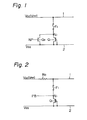
- Figure 1 shows a ROM for storing defective bits used in a conventioal semiconductor integrated circuit device (hereinafter, IC device).
- the illustrated ROM is provided with a fuse F 1 connected in series between power lines 1 and 2, a depletion transistor Q 1 , and a transistor Q 2 connected in parallel with the depletion transistor Q 1 .
- the gate of the depletion transistor Q 1 is connected to the source of the same transistor.
- the usual operational power for example, +5 V
- V SS for example, 0 V
- V SS for example, 0 V
- the voltage at the node N 1 becomes equal to V SS
- the voltage at the node N 1 becomes roughly equal to v CC . Therefore, by detecting the voltage at the node N 1 , it can be determined whether the fuse F 1 is written, i.e., whether the accessed bit is defective bit.
- the write signal NP is applied through a probing pad provided on the semiconductor chip. According to the ROM circuit of Fig. 1, the probing pad may be provided within the scribe lines.
- the probing pad when the probing pad is provided within the scribe lines, the probing pad, i.e., the gate of the transistor Q 2 , may short-circuit to the substrate potential V SS during wafer cutting. Even when such a short-circuit is caused, however, there is no effect whatsoever on the later operation of the ROM circuit.
- the maximum value of the current flowing through the fuse F 1 is limited by the G m , etc. of the transistor Q 2 , making it difficult to pass a sufficiently large current to the fuse F 1 .
- the transistor Q 2 is in the OFF state, the magnitude of the voltage applied between the power lines 1 and 2 is limited by the withstand voltage between the drain and source and between the drain and gate of the transistor Q 2 . Therefore, it is impossible to sufficiently raise the voltage of the high-voltage power Vpp.
- Figure 2 shown another conventional ROM circuit.
- the illustrated circuit instead of using the transistor Q 2 in the circuit of Fig. 1, connects the connection point N 1 of the fuse F 1 and the transistor Q 1 directly to the probing pad.
- a high voltage V Pp is supplied on the power line 1 and the node N1 is connected to the power line 2 through the probing pad PB.
- Figure 3 shows a R OM circuit used for an IC device according to an embodiment of the present invention.
- the ROM circuit of the figure is provided with a fuse F 1 and resistor R 1 connected in series between the power lines 1 and 2.
- the connection point between the fuse F l and the resistor R 1 i.e., the node N, is connected to a probing pad, not shown.
- the power line 1 has a resistance R 0 due to a bridge.
- the power line side of the fuse F 1 have a diffusion layer, and, thereby, there is a PN junction between the substrate and the power line, and that the other end of the fuse, i.e., the node N 2 , have no diffusion layer.
- the PN junction D 1 becomes forward-biased and the current flows by the route connecting substrate, PN junction D 1 , fuse F l , the node N 2 , probing pad. In this route, there are no factors restricting the current, and the necessary current sufficient for melting is passed to the fuse.
- Figure 4 shows a ROM circuit used for the IC device according to another embodiment of the present invention.
- the ROM circuit of the figure is provided with a depletion transistor Q 1 , fuse F 1 and resistor R 2 connected in series between the power lines 1 and 2.
- the gate and source of the depletion transistor Q 1 are mutually connected and are connected to the fuse F 1 and through the node N 3 .
- the connection point between the fuse F 1 and the resistor R 2 i.e., the node N 4 , is connected to a probing pad (not shown).
- the diode D 1 indicates a PN junction comprised by a P-type semiconductor substrate and a source electrode or other diffusion layer of a transistor Q 1 formed on the substrate.
- the probing pad connected to the node N 4 can, for example, be provided within the scribe lines.
- the PN junction D 1 comprised by the P-type semiconductor substrate and the N-type diffusion layer in the node N 3 is biased in the forward direction, current flows through the route connecting the substrate, PN junction D 1 , fuse F, , and probing pad, and the fuse is melted.
- the voltage supplied to the probing pad is almost completely, with the exception of the forward voltage component of the PN junction D 1 , supplied to the fuse F, , thereby enabling the fuse F 1 to be reliably cut.
- the node N 4 is connected to the power line 2.
- a resistance R 2 is provided.
- the end of the resistance R 2 on the node N 4 side must not have a diffusion layer so that melting current can be concentrated at the fuse F 1 during writing, but the end on the V ss side may have a diffusion layer so long as the value of the resistance R 2 is of a magnitude passing only an allowable writing current. In either case, the node N 4 is connected with the power line 2.
- the power line 1 is supplied with a power voltage V cc of, for example, 5 V, and the power line 2 is supplied with a power voltage V ss of, for example, 0 V. Therefore, if the fuse F 1 is melted, the potential of the node N 3 becomes V . If the fuse F 1 is not melted, the potential of the node N 3 becomes about V ss , i.e., the substrate potential.
- This detection circuit is comprised so as to have at its input terminal an MIS transistor with a gate connected to the node N 3 .
- the transistor Q 1 is used as a load resistance, but it is necessary that the value of this load resistance be made sufficiently large so as to reduce the power consumed by the ROM circuit.
- This load resistance can be realized by polycrystalline silicon, etc.
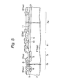
- Figure 5 is a cross-sectional view showing the concrete structure of the circuit of Fig. 4.
- the transistor Q 1 uses N +- type diffusion layers 4 and 5 formed on a P -type semiconductor substrate 3 as its drain and source and uses a conductive layer 6 made of polycrystalline silicon, etc. formed on the channel region between the N +- type diffusion layers 4 and 5 as its gate.
- the aluminum wiring 7 connected to the source diffusion layer 5 is connected with the gate 6 at a not shown portion, and the aluminum wiring layer 8 connected to the drain diffusion layer 4 is supplied with a power voltage V cc .
- the channel of the transistor Q 1 is formed to be considerably large so as to increased the resistance value.
- the diode D 1 is formed by the PN junction between the P -type substrate 3 and the source diffusion layer 5.
- the fuse F 1 is comprised by a polycrystalline silicon layer 10 provided on a field oxide layer 9 formed on the substrate 3.
- the resistance R 2 is comprised by a thin polycrystalline silicon layer 11 formed on the same field oxide layer 9.
- One end is connected to one end of the polycrystalline silicon layer 10 comprising the fuse F 1 by an aluminum wiring 12.
- aluminum wiring 13 connected to the other end of the polycrystalline silicon layer 11 is supplied with the substrate voltage V ss .
- the aluminum wiring 12 is connected to a probing pad (not shown). As shcwn in the figure, the node N 4 does not have a diffusion layer.
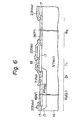
- Figure 6 is a cross-sectional view showing the construction of the ROM circuit of Fig. 4 using a CMOS construction.
- the construction of Fig. 6 utilizes, in place of the transistor Q, , a resistor R 3 comprised by a elongated N +- type diffusion layer 16 formed on a P-type well 15 formed on the N -type semiconductor substrate 14.
- the diode D 1 is comprised by a PN junction between the P-type well 15 and the N + -type diffusion layer 16.
- the fuse F 1 is comprised by a polycrystalline silicon layer 18 formed on the field oxide layer 17 in the same way as in the case of Fig. 5.
- the resistor R 2 is comprised by the elongated P +- type diffusion layer 19 formed on the N -type substrate 14.
- Reference numerals 20, 21, 22, and 23 are aluminum wiring.
- the diffusion layer 16 comprising the load resistor R 3 is formed on the P-type well 15, and the diffusion layer 19 comprising the resistor R 2 is formed on the substrate 14. It is also possible to directly form the diffusion layer 16 on the substrate 14 and to form the diffusion layer 19 on the P-type well.
- the object of the present invention can be achieved even if there is a diffusion layer 19 at the node N 4 . This is because, when N 4 is given a potential lower than V cc , the substrate 14 and the diffusion layer 19 become reversely biased and enter a nonconductance state, which is equivalent, in practice, to there being no diffusion layer.
- the P-type well 15 is supplied with the voltage V ss , for example, 0 V, while the aluminum wiring 22 connected to the prcbing pad is supplied with a voltage sufficiently lower than the voltage V .
- V ss the voltage
- the aluminum wiring 22 connected to the prcbing pad is supplied with a voltage sufficiently lower than the voltage V .
- Figure 7 shows a circuit wherein a ROM circuit having a plurality of fuses is comprised by a CMOS construction in the same way as Fig. 6.
- the ROM circuit of the figure has nine fuses F 01 , F 02 , ..., F 09 , the ends of these fuses being connected through the contact windows 24-1, 24-2, ..., 24-9 to the N +- type diffusion layer 25-1, 25-2, ..., 25-9.
- the N +- type diffusion layers 25-1, 25-2, and 25-3 are formed on the P-type well 26-1
- the N +- type diffusion layers 25-4, 25-5, and 25-6 are formed on the P-type well 26-2
- the N + -type diffusion layers 25-7, 25-8, and 25-9 are formed on the P-type well 26-3.
- the end portions of the contact windows 24-1, 24-2, ..., 24-9 of the N +- type diffusion layers 25-1, 25-2, ..., 25-9 comprise diodes D 01 , D 11 , ..., D 81 , with the corresponding P-type wells and are given a wide shape, enlarging the junction area with the corresponding P-type wells so as to enable the flow of a large current.
- the other ends of the N + -type diffusion layers 25-1, 25-2, ..., 25-9 are supplied with the power voltage V cc .
- the probing pads P 0 , P 1 , P 2 ' P 3 , P 4 , P 5 are provided for the nine fuses F 01 , F 02 , ..., FO g.
- the probing pads P 0 , P 1 , and P 2 are connected to the P-type wells 26-1, 26-2, and 26-3.
- the probing pad P 3 is connected to the other ends of the fuses F 01 , F 04 , and F 07
- the probing pad P 4 is connected to the other end of the fuses F 02 , F 05 ' and F 08
- the probing pad P 5 is connected to the other end of the fuses F 03 , F 06 , and F 09 .
- Figures 8A and 8B show the construction where the probing pads of the IC device are provided according to an embodiment of the present invention within the scribe line portion B.
- Figure 8A is a plan view
- Fig. 8B is a cross-sectional view on the line A-A.
- the portion shown by hatched lines is the aluminum wiring layer 27, for example, connected to the node N 4 in the circuit of Fig. 4.
- Reference numeral 28 is a cover insulation film and is formed for the scribe line portion B except the portion of the aluminum wiring layer 27 comprising the probing pads.
- 29 is a semiconductor substrate, 30 a field oxide layer, and 31 an insulation film for insulation the aluminum wiring layer and the polycrystalline silicon layer comprising the gate electrodes, etc.
- Reference numeral 39 is a diffusion layer and, as shown in the figure, the probing pad portions have no diffusion layers.
- Figures 9A and 9B show the construction of an optimal PN junction portion using the ROM circuit according to the above-mentioned embodiment.
- 32 shows a P-type semiconductor substrate or P-type well or other P-type region, and 33 an N-type diffusion layer formed on the P-type region 42.
- Reference numeral 34 is an aluminum wiring layer connected to the N-type diffusion layer 33 in the contact window 35 and is, for example, connected to one end of the fuse F l .
- the N-type diffusion layer 33 is connected to the source, etc. of, for example, the transistor Q l .
- Reference numeral 36 is an aluminum wiring layer connected to the P-type region 32 in the contact windows 37 and is supplied with, for example, the power voltage V ss .
- V ss the power voltage
- the area of the junction portion between the P-type region 32 and the N-type diffusion layer 33 is made large and an aluminum wiring layer is provided so as to surround the N-type region 33. Therefore, it is possible to reduce the voltage drop of the PN junction portion and to pass a large current.
- the present invention makes it possible to supply a voltage and current with a sufficient leeway to fuses without limitation due to the withstand voltage, allowable current, etc. of the transistors and other circuit elements and therefore, enables reliable melting of fuses. Further, it enables the provision of the probing pads within the scribe line portion and further enables provision of a fewer number of probing pads than fuses for achievement of the objective. Therefore, it enables reduction of the occupied area of the ROM circuit and improvement of the degree of integration of the IC device.
Landscapes
- Design And Manufacture Of Integrated Circuits (AREA)
- Semiconductor Integrated Circuits (AREA)
- Testing Or Measuring Of Semiconductors Or The Like (AREA)
- Read Only Memory (AREA)
Applications Claiming Priority (2)
| Application Number | Priority Date | Filing Date | Title |
|---|---|---|---|
| JP229052/83 | 1983-12-06 | ||
| JP58229052A JPS60121599A (ja) | 1983-12-06 | 1983-12-06 | 集積回路装置 |
Publications (3)
| Publication Number | Publication Date |
|---|---|
| EP0145595A2 true EP0145595A2 (fr) | 1985-06-19 |
| EP0145595A3 EP0145595A3 (en) | 1987-10-21 |
| EP0145595B1 EP0145595B1 (fr) | 1990-05-16 |
Family
ID=16885987
Family Applications (1)
| Application Number | Title | Priority Date | Filing Date |
|---|---|---|---|
| EP84402512A Expired - Lifetime EP0145595B1 (fr) | 1983-12-06 | 1984-12-06 | Dispositif de circuit intégré |
Country Status (5)
| Country | Link |
|---|---|
| US (1) | US4903111A (fr) |
| EP (1) | EP0145595B1 (fr) |
| JP (1) | JPS60121599A (fr) |
| KR (1) | KR900006150B1 (fr) |
| DE (1) | DE3482294D1 (fr) |
Cited By (1)
| Publication number | Priority date | Publication date | Assignee | Title |
|---|---|---|---|---|
| EP1079430A3 (fr) * | 1999-08-26 | 2002-10-16 | Fujitsu Limited | Procédé de fabricaiton d'un composant semi-conducteur |
Families Citing this family (23)
| Publication number | Priority date | Publication date | Assignee | Title |
|---|---|---|---|---|
| JPS6246496A (ja) * | 1985-08-23 | 1987-02-28 | Sony Corp | 固定記憶装置の書き込み方法 |
| US5047826A (en) * | 1989-06-30 | 1991-09-10 | Texas Instruments Incorporated | Gigaohm load resistor for BICMOS process |
| FR2655762B1 (fr) * | 1989-12-07 | 1992-01-17 | Sgs Thomson Microelectronics | Fusible mos a claquage d'oxyde tunnel programmable. |
| NL9001558A (nl) * | 1990-07-09 | 1992-02-03 | Philips Nv | Stabiel dissipatie-arm referentiecircuit. |
| US5270983A (en) * | 1990-09-13 | 1993-12-14 | Ncr Corporation | Single element security fusible link |
| US5539402A (en) * | 1992-08-03 | 1996-07-23 | The United States Of America As Represented By The Administrator Of The National Aeronautics And Space Administration | System for memorizing maximum values |
| US5963825A (en) * | 1992-08-26 | 1999-10-05 | Hyundai Electronics America | Method of fabrication of semiconductor fuse with polysilicon plate |
| DE4336562A1 (de) * | 1993-10-27 | 1995-05-04 | Itt Ind Gmbh Deutsche | Kurzschlußstruktur für CMOS-Schaltungen |
| US5444650A (en) * | 1994-01-25 | 1995-08-22 | Nippondenso Co., Ltd. | Semiconductor programmable read only memory device |
| US6100747A (en) * | 1994-05-30 | 2000-08-08 | Stmicroelectronics, S.R.L. | Device for selecting design options in an integrated circuit |
| JPH08222710A (ja) * | 1995-02-17 | 1996-08-30 | Mitsubishi Electric Corp | 半導体装置 |
| US5636172A (en) * | 1995-12-22 | 1997-06-03 | Micron Technology, Inc. | Reduced pitch laser redundancy fuse bank structure |
| RU2172539C2 (ru) * | 1996-02-09 | 2001-08-20 | Сименс Акциенгезелльшафт | Разъединяемый соединительный мостик (разрушаемая перемычка) и соединяемый разрыв проводника (восстанавливаемая перемычка), а также способ изготовления и активирования разрушаемой перемычки и восстанавливаемой перемычки |
| US5939934A (en) * | 1996-12-03 | 1999-08-17 | Stmicroelectronics, Inc. | Integrated circuit passively biasing transistor effective threshold voltage and related methods |
| EP0856893B1 (fr) | 1996-12-31 | 2002-05-02 | STMicroelectronics, Inc. | Structure et dispositif pour la sélection d'options de conception dans un circuit intégré |
| US6972612B2 (en) * | 1999-06-22 | 2005-12-06 | Samsung Electronics Co., Ltd. | Semiconductor device with malfunction control circuit and controlling method thereof |
| JP2002033361A (ja) * | 2000-07-17 | 2002-01-31 | Mitsumi Electric Co Ltd | 半導体ウェハ |
| KR100831799B1 (ko) * | 2004-04-08 | 2008-05-28 | 가부시끼가이샤 르네사스 테크놀로지 | 반도체기억장치 |
| US7372726B2 (en) * | 2004-04-08 | 2008-05-13 | Renesas Technology Corp. | Semiconductor memory |
| US7629234B2 (en) * | 2004-06-18 | 2009-12-08 | Electro Scientific Industries, Inc. | Semiconductor structure processing using multiple laterally spaced laser beam spots with joint velocity profiling |
| JP4685388B2 (ja) * | 2004-09-06 | 2011-05-18 | Okiセミコンダクタ株式会社 | 半導体装置 |
| US7531886B2 (en) * | 2006-07-06 | 2009-05-12 | International Business Machines Corporation | MOSFET fuse programmed by electromigration |
| US20230253271A1 (en) * | 2022-02-04 | 2023-08-10 | Skyworks Solutions, Inc. | Semiconductor wafer having contact pads configured to act as probe pads |
Family Cites Families (13)
| Publication number | Priority date | Publication date | Assignee | Title |
|---|---|---|---|---|
| DE2350949A1 (de) * | 1973-10-11 | 1975-04-24 | Licentia Gmbh | Datenspeicher- und datenspeicheransteuerschaltung |
| JPS5122341A (ja) * | 1974-08-19 | 1976-02-23 | Fujitsu Ltd | Handotaiyomitorisenyokiokusochino shikenhoho |
| US4045310A (en) * | 1976-05-03 | 1977-08-30 | Teletype Corporation | Starting product for the production of a read-only memory and a method of producing it and the read-only memory |
| JPS5737358Y2 (fr) * | 1977-06-07 | 1982-08-17 | ||
| JPS54139496A (en) * | 1978-04-21 | 1979-10-29 | Hitachi Ltd | Mos semiconductor load element |
| US4210875A (en) * | 1978-12-29 | 1980-07-01 | Harris Corporation | Integrated amplifier with adjustable offset voltage |
| JPS5763854A (en) * | 1980-10-07 | 1982-04-17 | Toshiba Corp | Semiconductor device |
| US4446534A (en) * | 1980-12-08 | 1984-05-01 | National Semiconductor Corporation | Programmable fuse circuit |
| US4446475A (en) * | 1981-07-10 | 1984-05-01 | Motorola, Inc. | Means and method for disabling access to a memory |
| EP0076967B1 (fr) * | 1981-10-09 | 1987-08-12 | Kabushiki Kaisha Toshiba | Dispositif semi-conducteur comprenant un élément fusible |
| JPS58131764A (ja) * | 1982-01-29 | 1983-08-05 | Toshiba Corp | ヒユ−ズ溶断形半導体記憶装置 |
| US4417154A (en) * | 1982-02-08 | 1983-11-22 | Motorola, Inc. | Circuit for applying a high voltage signal to a fusible link |
| JPS59105354A (ja) * | 1982-12-09 | 1984-06-18 | Toshiba Corp | 半導体装置 |
-
1983
- 1983-12-06 JP JP58229052A patent/JPS60121599A/ja active Granted
-
1984
- 1984-12-06 KR KR1019840007696A patent/KR900006150B1/ko not_active Expired
- 1984-12-06 DE DE8484402512T patent/DE3482294D1/de not_active Expired - Lifetime
- 1984-12-06 EP EP84402512A patent/EP0145595B1/fr not_active Expired - Lifetime
-
1988
- 1988-10-25 US US07/265,275 patent/US4903111A/en not_active Expired - Fee Related
Cited By (2)
| Publication number | Priority date | Publication date | Assignee | Title |
|---|---|---|---|---|
| EP1079430A3 (fr) * | 1999-08-26 | 2002-10-16 | Fujitsu Limited | Procédé de fabricaiton d'un composant semi-conducteur |
| EP1833086A3 (fr) * | 1999-08-26 | 2008-08-13 | Fujitsu Ltd. | Procédé de fabrication d'un dispositif à semi-conducteur |
Also Published As
| Publication number | Publication date |
|---|---|
| JPS60121599A (ja) | 1985-06-29 |
| US4903111A (en) | 1990-02-20 |
| DE3482294D1 (de) | 1990-06-21 |
| EP0145595A3 (en) | 1987-10-21 |
| KR850005156A (ko) | 1985-08-21 |
| KR900006150B1 (ko) | 1990-08-24 |
| JPS641880B2 (fr) | 1989-01-12 |
| EP0145595B1 (fr) | 1990-05-16 |
Similar Documents
| Publication | Publication Date | Title |
|---|---|---|
| US4903111A (en) | Integrated circuit device | |
| CA1147818A (fr) | Circuit integre comportant des circuits generateurs de signaux de commande | |
| US7910922B2 (en) | Semiconductor integrated circuit device and manufacture thereof | |
| US5001529A (en) | Semiconductor device having protection circuit | |
| US4855613A (en) | Wafer scale integration semiconductor device having improved chip power-supply connection arrangement | |
| US20030042888A1 (en) | Semiconductor integrated circuit allowing proper detection of pin contact failure | |
| US5410163A (en) | Semi-conductor integrated circuit device including connection and disconnection mechanisms to connect and disconnect monitor circuit and semiconductor integrated circuit from each other | |
| KR100222623B1 (ko) | 입력 보호 회로 및 이를 이용한 반도체 장치 | |
| US20050274966A1 (en) | Fuse and write method for fuse | |
| JP2007200387A (ja) | 半導体装置及びその製造方法 | |
| JP2002033361A (ja) | 半導体ウェハ | |
| JPH06232373A (ja) | 半導体メモリ装置 | |
| JPH03290900A (ja) | 半導体メモリ装置 | |
| KR100294019B1 (ko) | 반도체칩의정전기보호용트랜지스터 | |
| US5068605A (en) | Semiconductor integrated circuit device and method of testing the same | |
| JP3758251B2 (ja) | 半導体記憶装置 | |
| JP3495835B2 (ja) | 半導体集積回路装置及びその検査方法 | |
| US20060255823A1 (en) | Semiconductor device, method for testing the same and IC card | |
| CN105144360A (zh) | 用于监视半导体制作的方法及设备 | |
| JPS59201298A (ja) | 半導体記憶装置 | |
| KR100463722B1 (ko) | 스태틱 랜덤 액세스 메모리 장치 | |
| KR100197572B1 (ko) | 퓨즈소자를 가지는 반도체 직접회로 | |
| JPS6257260B2 (fr) | ||
| CN122029960A (zh) | 半导体装置 | |
| JPH05267579A (ja) | 半導体集積回路の入力保護回路 |
Legal Events
| Date | Code | Title | Description |
|---|---|---|---|
| PUAI | Public reference made under article 153(3) epc to a published international application that has entered the european phase |
Free format text: ORIGINAL CODE: 0009012 |
|
| AK | Designated contracting states |
Designated state(s): DE FR GB |
|
| PUAL | Search report despatched |
Free format text: ORIGINAL CODE: 0009013 |
|
| AK | Designated contracting states |
Kind code of ref document: A3 Designated state(s): DE FR GB |
|
| 17P | Request for examination filed |
Effective date: 19871121 |
|
| 17Q | First examination report despatched |
Effective date: 19880728 |
|
| GRAA | (expected) grant |
Free format text: ORIGINAL CODE: 0009210 |
|
| AK | Designated contracting states |
Kind code of ref document: B1 Designated state(s): DE FR GB |
|
| REF | Corresponds to: |
Ref document number: 3482294 Country of ref document: DE Date of ref document: 19900621 |
|
| ET | Fr: translation filed | ||
| PGFP | Annual fee paid to national office [announced via postgrant information from national office to epo] |
Ref country code: GB Payment date: 19901123 Year of fee payment: 7 |
|
| PGFP | Annual fee paid to national office [announced via postgrant information from national office to epo] |
Ref country code: DE Payment date: 19910222 Year of fee payment: 7 |
|
| PLBE | No opposition filed within time limit |
Free format text: ORIGINAL CODE: 0009261 |
|
| STAA | Information on the status of an ep patent application or granted ep patent |
Free format text: STATUS: NO OPPOSITION FILED WITHIN TIME LIMIT |
|
| 26N | No opposition filed | ||
| PG25 | Lapsed in a contracting state [announced via postgrant information from national office to epo] |
Ref country code: GB Effective date: 19911206 |
|
| GBPC | Gb: european patent ceased through non-payment of renewal fee | ||
| PG25 | Lapsed in a contracting state [announced via postgrant information from national office to epo] |
Ref country code: FR Effective date: 19920831 |
|
| PG25 | Lapsed in a contracting state [announced via postgrant information from national office to epo] |
Ref country code: DE Effective date: 19920901 |
|
| REG | Reference to a national code |
Ref country code: FR Ref legal event code: ST |
|
| PG25 | Lapsed in a contracting state [announced via postgrant information from national office to epo] |
Ref country code: FR Effective date: 19901231 |