EP0146345A2 - S-Korrekturschaltung mit geschaltetem Kondensator - Google Patents
S-Korrekturschaltung mit geschaltetem Kondensator Download PDFInfo
- Publication number
- EP0146345A2 EP0146345A2 EP84308666A EP84308666A EP0146345A2 EP 0146345 A2 EP0146345 A2 EP 0146345A2 EP 84308666 A EP84308666 A EP 84308666A EP 84308666 A EP84308666 A EP 84308666A EP 0146345 A2 EP0146345 A2 EP 0146345A2
- Authority
- EP
- European Patent Office
- Prior art keywords
- capacitor
- deflection
- interval
- circuit
- transistor
- Prior art date
- Legal status (The legal status is an assumption and is not a legal conclusion. Google has not performed a legal analysis and makes no representation as to the accuracy of the status listed.)
- Granted
Links
Images

Classifications
-
- H—ELECTRICITY
- H04—ELECTRIC COMMUNICATION TECHNIQUE
- H04N—PICTORIAL COMMUNICATION, e.g. TELEVISION
- H04N3/00—Scanning details of television systems; Combination thereof with generation of supply voltages
- H04N3/10—Scanning details of television systems; Combination thereof with generation of supply voltages by means not exclusively optical-mechanical
- H04N3/16—Scanning details of television systems; Combination thereof with generation of supply voltages by means not exclusively optical-mechanical by deflecting electron beam in cathode-ray tube, e.g. scanning corrections
- H04N3/22—Circuits for controlling dimensions, shape or centering of picture on screen
- H04N3/23—Distortion correction, e.g. for pincushion distortion correction, S-correction
- H04N3/233—Distortion correction, e.g. for pincushion distortion correction, S-correction using active elements
Definitions
- This invention relates to correction of cathode ray tube geometry distortion, and in particular, to deflection current S-correction for cathode ray tubes having complex correction requirements.
- the cathode ray tube of a video display apparatus incorporates an electron gun assembly which produces an electron beam or beams.
- the beams are deflected or scanned to form a raster on a phosphor display screen located on the inside surface of the front panel of the tube.
- the radius of curvature of the front panel is greater than the distance from the deflection center of the electron beams to the center of the display screen (i.e., the deflection distance). Because of the difference in radii, the electron beams travel a greater distance to the edges of the display screen than to the center of the screen. For a given amount of deflection, therefore, the beams will traverse a greater distance on the display screen near the edges than at the center of the screen.
- the previously described geometry correction may not be sufficient.
- insufficient correction may occur with tubes having a front panel with a spherical radius of curvature greater than a conventional tube, or with tubes having a complex or compound faceplate curvature with multiple radii, such as is described in U.S. Patent Application Serial Number 469,775, filed February 25, 1983, in the names of D'Amato et al. and entitled "Cathode Ray Tube Having Different Curvatures Along Major and Minor Axes" corresponding to German O LS 3406787 and GB 2136199A.
- a single S-shaping capacitor may not be able to provide the desired amount of correction at all screen locations, and may provide too much or too little correction at different regions of the screen.
- the present invention is directed to an S-correction circuit that provides effective correction for tubes having large deflection angles or complex faceplate contours.
- a horizontal or line deflection circuit comprises a horizontal deflection winding.and a circuit for providing a deflection current in the winding, which current defines a trace and a retrace interval.
- a first capacitor is coupled to the deflection winding and provides symmetrical linearity correction to the deflection current.
- a circuit couples a second capacitor to the deflection winding during a portion of the trace interval in order to modify the amount of linearity correction provided to the deflection current.
- FIGURE 1 is a schematic and block diagram af a portion of a television receiver incorporating a correction circuit in accordance with an aspect of the present invention.
- FIGURES 2 and 3 illustrate waveforms associated with the circuit of FIGURE 1.
- FIGURE 1 there is shown a portion of a video display apparatus, such as a television receiver, incorporating a horizontal or line deflection circuit 10.
- the horizontal deflection circuit 10 includes horizontal oscillator and driver circuits 11 which apply switching signals to the base of a horizontal output transistor 12. Coupled to the horizontal output transistor 12 is a damper diode 13, a retrace capacitor 14, a horizontal deflection winding 15 and an S-shaping capacitor 16. Power is provided to the horizontal output circuit 10 from a power supply of the order of +130 volts via a primary winding 17 of a power transformer 20.
- Transformer 20 generates a source of high voltage at a terminal 22 via windings 21.
- the high voltage potential of the order of 30 KV, is applied to the anode or ultor terminal of a kinescope (not shown).
- Transformer 20 also provides power to other receiver circuits. This is illustratively shown in FIGURE 1 by secondary winding 23, filter capacitor 24 and rectifying diode 25, which provides a voltage level designated +V at a terminal 26.
- Horizontal deflection circuit 10 generates a sawtooth current in horizontal deflection winding 15 which in turn produces a deflection field which deflects the electron beams of the kinescope.
- the electron beams are deflected to form a raster on the display screen of the kinescope. Since the electron beams are deflected farther to the corners of the raster than to the edges, the sides of the raster will appear inwardly bowed or pincushion shaped.
- horizontal deflection circuit 10 incorporates a diode modulator correction circuit 30 which modulates the horizontal deflection current at a vertical deflection rate in a parabolic manner.
- Diode modulator circuit 30 incorporates a vertical parabola generator 31 which applies a parabolic vertical rate signal to a transistor 32.
- Diode modulator circuit 30 also comprises a modulator capacitor 33, a modulator inductor 34, a modulator retrace capacitor 35 and a modulator diode 36. Conduction of transistor 32 controls the voltage across modulator capacitor 33 in order to vary the modulator capacitor voltage in a parabolic manner. This in turn varies the horizontal deflection trace voltage in order to provide correction of side pincushion distortion.
- FIGURE 1 illustrates an S-correction circuit 37 which provides effective S-correction for picture tubes having complex S-correction requirements.
- S-correction circuit 37 includes a switching transistor 40, a diode 41 and a capacitor 42. Switching of transistor 40 into conduction has the effect of placing capacitor 42 in parallel with S-shaping capacitor 16, thereby increasing the amount of circuit S-shaping capacitance.
- Two values of S-shaping capacitance may be presented to the horizontal deflection circuit; namely, the value of capacitor 16 and the value of the parallel combination of capacitors 16 and 42. This allows the amount of S-shaping correction to be changed for different portions of the horizontal deflection interval.
- Switching pulses are applied to the base of transistor 40 via a transformer 43.
- Transformer 43 permits the application of a fixed amplitude pulse to the base of transistor 40 independent of the emitter voltage, which follows the pincushion correcting parabola voltage produced by diode modulator correction circuit 30.
- S-correction circuitry 37 of FIGURE 1 produces switching pulses for transistor 40 which may be modulated with respect to their time of occurrence within the horizontal deflection interval.
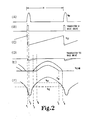
- Horizontal retrace derived pulses shown in FIGURE 2A, produced across winding 44 of transformer 20, are applied to differentiator circuits 45 and 46.
- Differentiator circuit 45 comprising capacitor 49, resistors 47 and 48, and diode 50, differentiates the leading edges of the horizontal rate pulses from winding 44 in order to produce a short duration pulse, illustratively shown in FIGURE 2B, that is used to turn transistor 51 on for approximately 5 microseconds.
- Capacitor 52 together with resistor 53 and the +230 volt supply, form a ramp generator. Turn-on of transistor 51 causes capacitor 52 to discharge through transistor 51 to ground, thereby resetting the ramp. Capacitor 52 discharges very quickly, as shown in FIGURE 2C, so that it is completely discharged before transistor 51 is turned off. 'When transistor'51 is turned off, capacitor 52 charges through resistor 53 to form a horizontal rate ramp signal, shown in FIGURE 2C, that is applied via variable resistor 54 and resistor 55 to the base of a transistor 56. Variable resistor 54 controls the amplitude of the ramp signal that is applied to transistor 56.
- Differentiator 46 produces a short duration pulse which turns transistor 57 on and off coincident with the switching of transistor 51. Conduction of transistor 57 rapidly removes the charge from the base region of transistor 56 so that transistor 56 turns off very quickly when the horizontal rate ramp is reset.
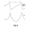
- Vertical deflection circuit 60 in addition to generating a sawtooth vertical deflection current, shown in FIGURE 3A, for a vertical deflection winding (not shown), provides a vertical rate parabolic voltage signal which is inverted by transistor 61 to form a signal as shown in FIGURE 3B.
- This vertical rate parabolic voltage is added to the horizontal rate ramp voltage to form a signal, as shown in FIGURE 2D, that is applied to the base of transistor 56 through resistor 58.
- the vertical parabola voltage has the effect of changing the dc level of the horizontal ramp, as illustrated by the solid and dashed waveforms of FIGURE 2D. This variation in dc level over the course of the vertical deflection interval modulates the turn-on time of transistor 56 at a vertical rate.
- Variable resistor 62 is adjustable to set the dc bias on the base of transistor 56 in order to control the point at which transistor 56 switches.
- the circuit of FIGURE 1 is illustratively configured to cause transistor 56 to turn on earlier in the horizontal deflection interval near the top and bottom of the scanned raster; i.e., where the vertical rate parabolic voltage is greatest. This is shown by the dashed waveform in FIGURE 2D.
- a different cathode ray tube faceplate contour may, however, require a different modulation in which transistor 56 would turn on later during horizontal deflection intervals near the top and bottom of the raster. Such a requirement could be satisfied, for example, by removing transistor 61, which would eliminate the inversion of the parabolic voltage signal from vertical deflection circuit 60.
- Other circuit modifications to satisfy particular modulation requirements are, of course, possible.
- Conduction of transistor 56 provides a low impedance current path which clamps the base drive signal, as shown in FIGURE 2D. Conduction of transistor 56 also causes transistor 63 to conduct, via switching of amplifying transistor 64. Conduction of transistor 63 causes current to flow in winding 66 of transformer 43 from the +30 volt supply, through winding 66 and transistor 63 to ground. This causes a current to flow in winding 65 of transformer 43 which, because of the coupling polarity of windings 65 and 66, will turn transistor 40 off. As can be seen in FIGURE 2E, transistor 40 is turned off at time t 3 in response to the dashed waveform of FIGURE 2D,and at time t 4 in response to the solid waveform of FIGURE 2D.
- the turn-off time of transistor 40 will occur during the first half of the horizontal trace interval. With transistor 40 turned off, the voltage across capacitor 42 will remain constant, as shown in FIGURE 2F, while the voltage across S-shaping capacitor 16 continues to rise, as shown also in FIGURE 2F. During the second half of the horizontal trace interval, the voltage across capacitor 16 begins to decrease. When the voltage across capacitor 16 equals the voltage across capacitor 42, diode 41 will begin to conduct, and capacitor 42 begins to discharge, thereby influencing the S-correction of the deflection current. Diode 41 will continue to conduct until the center of the horizontal retrace interval, when the direction of deflection current reverses.
- transistor 40 Resetting of the horizontal rate ramp voltage generated across capacitor 52 causes transistor 40 to begin conducting which in turn causes capacitor 42 to charge again, until transistor 40 is turned off as previously described. It is important that transistor 40 be turned on when its collector voltage is near zero in order to prevent a potentially damaging current surge in the transistor when it is turned on. To accomplish this objective, transistor 40 should be turned on when diode 41 is conducting.
- the charge on capacitor 42 determined by the length of conduction of transistor 40, will also determine the time at which diode 41 begins to conduct after transistor 40 is turned off.
- the charge and discharge intervals of capacitor 42 hence the intervals when capacitor 42 contributes to S-correction, are symmetrical about the center of the horizontal trace interval for both transistor 40 turn off times of either t 3 or t 4' This occurs because the time at which diode 41 begins to conduct will always occur when the voltage level across capacitor 16 is equal to the same level as it was when transistor 40 was turned off. Symmetry of S-correction about the center of horizontal trace is therefore achieved regardless of the time at which transistor 40 is turned off.
- the previously described S-correction circuit therefore provides switchable amounts of correction during a given line deflection interval.
- the point at which the S-correction switching occurs in a given line may be controlled in order to increase the flexibility of the correction circuit.
Landscapes
- Engineering & Computer Science (AREA)
- Multimedia (AREA)
- Signal Processing (AREA)
- Details Of Television Scanning (AREA)
Applications Claiming Priority (2)
| Application Number | Priority Date | Filing Date | Title |
|---|---|---|---|
| US562246 | 1983-12-16 | ||
| US06/562,246 US4533855A (en) | 1983-12-16 | 1983-12-16 | Switched capacitor S-correction circuit |
Publications (3)
| Publication Number | Publication Date |
|---|---|
| EP0146345A2 true EP0146345A2 (de) | 1985-06-26 |
| EP0146345A3 EP0146345A3 (en) | 1985-08-07 |
| EP0146345B1 EP0146345B1 (de) | 1988-07-06 |
Family
ID=24245449
Family Applications (1)
| Application Number | Title | Priority Date | Filing Date |
|---|---|---|---|
| EP84308666A Expired EP0146345B1 (de) | 1983-12-16 | 1984-12-13 | S-Korrekturschaltung mit geschaltetem Kondensator |
Country Status (7)
| Country | Link |
|---|---|
| US (1) | US4533855A (de) |
| EP (1) | EP0146345B1 (de) |
| JP (1) | JPS60148282A (de) |
| DE (1) | DE3472609D1 (de) |
| GB (1) | GB2151866B (de) |
| HK (1) | HK23593A (de) |
| MY (1) | MY100455A (de) |
Cited By (5)
| Publication number | Priority date | Publication date | Assignee | Title |
|---|---|---|---|---|
| US5315216A (en) * | 1991-12-21 | 1994-05-24 | U.S. Philips Corporation | Television picture display device and circuit for horizontal deflection in such a television picture display device |
| EP0664644A3 (en) * | 1994-01-25 | 1995-08-16 | Rca Thomson Licensing Corp | Inner raster distortion correction circuit. |
| EP0823812A3 (de) * | 1996-08-07 | 1998-03-18 | Victor Company Of Japan, Ltd. | Horizontale S-Form-Korrektionsschaltung |
| EP0844787A1 (de) * | 1996-11-21 | 1998-05-27 | Victor Company Of Japan, Ltd. | Dynamisches Fokussierungsgerät für Kathodenstrahlröhren-Darstellungsvorrichtung |
| EP0844786A1 (de) * | 1996-11-25 | 1998-05-27 | Lg Electronics Inc. | S-Form Korrekturschaltung für horizontale Ablenkung mit veränderlicher Kapazität |
Families Citing this family (15)
| Publication number | Priority date | Publication date | Assignee | Title |
|---|---|---|---|---|
| IT1217297B (it) * | 1985-05-29 | 1990-03-22 | Sgs Thomson Microelectronics | Circuito elettronico per la correzione a s della rampa di scansione verticale in un apparecchio televisivo |
| US4645985A (en) * | 1986-02-26 | 1987-02-24 | Rca Corporation | S-correction circuit for a video display |
| US4709193A (en) * | 1986-05-30 | 1987-11-24 | Rca Corporation | S-capacitance switching circuit for a video display |
| FR2603442B1 (fr) * | 1986-09-02 | 1988-11-10 | Radiotechnique Ind & Comm | Circuit de balayage lignes avec correction dynamique de s |
| US4871951A (en) * | 1987-10-23 | 1989-10-03 | U.S. Philips Corporation | Picture display device including a line synchronizing circuit and a line deflection circuit |
| DE69318999T2 (de) * | 1992-02-25 | 1999-03-18 | Matsushita Electric Industrial Co., Ltd., Kadoma, Osaka | Schaltung zur Unterdrückung des Moire-Effekts |
| JP2764140B2 (ja) * | 1992-09-02 | 1998-06-11 | セイコーインスツルメンツ株式会社 | Crt管面補正用アナログ波形発生装置 |
| JPH09331466A (ja) * | 1996-06-11 | 1997-12-22 | Sony Corp | 水平直線性補正回路 |
| US5877599A (en) * | 1996-10-11 | 1999-03-02 | National Semiconductor Corporation | Vertical and horizontal scanning correction system for video display |
| JP3832090B2 (ja) * | 1998-05-07 | 2006-10-11 | ソニー株式会社 | 水平偏向回路 |
| US6274989B1 (en) | 1999-01-12 | 2001-08-14 | Walter Truskalo | Dynamic damping clamper arrangement associated with s-shaping capacitor |
| US6208093B1 (en) * | 1999-02-08 | 2001-03-27 | Thomson Licensing S.A. | Selectable clampers for an S-shaping voltage of a video display |
| US6586895B2 (en) | 2001-05-08 | 2003-07-01 | Thomson Licensing S.A. | Raster distortion correction circuit |
| US6614193B2 (en) | 2001-08-31 | 2003-09-02 | Thomson Licensing S.A. | Deflection current modulation circuit |
| DE102011009162A1 (de) | 2011-01-22 | 2012-07-26 | Markus Rehm | Gesteuerte Großsignal Kapazität und Induktivität |
Family Cites Families (8)
| Publication number | Priority date | Publication date | Assignee | Title |
|---|---|---|---|---|
| NL157475B (nl) * | 1970-07-18 | 1978-07-17 | Philips Nv | Beeldweergeefinrichting met een schakeling voor het opwekken van een beeldregelfrequentie in hoofdzaak zaagtandvormige afbuigstroom. |
| JPS5542527Y2 (de) * | 1975-07-03 | 1980-10-06 | ||
| US4019093A (en) * | 1975-10-09 | 1977-04-19 | Gte Sylvania Incorporated | Horizontal dynamic damper circuitry |
| US4181874A (en) * | 1977-12-12 | 1980-01-01 | Rca Corporation | Television S-correction circuit with improved linearity |
| US4176303A (en) * | 1978-05-17 | 1979-11-27 | Rca Corporation | Television S-correction linearity device |
| GB2044029B (en) * | 1978-09-12 | 1982-11-10 | Elliott Brothers London Ltd | Circuit for driving deflection coil |
| US4329729A (en) * | 1980-06-23 | 1982-05-11 | Rca Corporation | Side pincushion modulator circuit with overstress protection |
| JPS5745733U (de) * | 1980-08-30 | 1982-03-13 |
-
1983
- 1983-12-16 US US06/562,246 patent/US4533855A/en not_active Expired - Lifetime
-
1984
- 1984-12-13 DE DE8484308666T patent/DE3472609D1/de not_active Expired
- 1984-12-13 EP EP84308666A patent/EP0146345B1/de not_active Expired
- 1984-12-13 JP JP59264361A patent/JPS60148282A/ja active Granted
- 1984-12-13 GB GB08431540A patent/GB2151866B/en not_active Expired
-
1986
- 1986-12-10 MY MYPI86000189A patent/MY100455A/en unknown
-
1993
- 1993-03-18 HK HK235/93A patent/HK23593A/xx not_active IP Right Cessation
Cited By (9)
| Publication number | Priority date | Publication date | Assignee | Title |
|---|---|---|---|---|
| US5315216A (en) * | 1991-12-21 | 1994-05-24 | U.S. Philips Corporation | Television picture display device and circuit for horizontal deflection in such a television picture display device |
| EP0664644A3 (en) * | 1994-01-25 | 1995-08-16 | Rca Thomson Licensing Corp | Inner raster distortion correction circuit. |
| US5661375A (en) * | 1994-01-25 | 1997-08-26 | Rca Thomson Licensing Corporation | Inner raster distortion correction circuit |
| EP0823812A3 (de) * | 1996-08-07 | 1998-03-18 | Victor Company Of Japan, Ltd. | Horizontale S-Form-Korrektionsschaltung |
| US5962993A (en) * | 1996-08-07 | 1999-10-05 | Victor Company Of Japan, Ltd. | Horizontal S-shape correction circuit |
| EP0844787A1 (de) * | 1996-11-21 | 1998-05-27 | Victor Company Of Japan, Ltd. | Dynamisches Fokussierungsgerät für Kathodenstrahlröhren-Darstellungsvorrichtung |
| US5981952A (en) * | 1996-11-21 | 1999-11-09 | Victor Company Of Japan, Ltd. | Dynamic focusing apparatus for cathode-ray tube device |
| EP0844786A1 (de) * | 1996-11-25 | 1998-05-27 | Lg Electronics Inc. | S-Form Korrekturschaltung für horizontale Ablenkung mit veränderlicher Kapazität |
| US5955848A (en) * | 1996-11-25 | 1999-09-21 | Lg Electronics Inc. | Horizontal deflection S-shaped correction signal circuit with variable capacitance |
Also Published As
| Publication number | Publication date |
|---|---|
| JPS60148282A (ja) | 1985-08-05 |
| GB2151866B (en) | 1987-03-25 |
| GB2151866A (en) | 1985-07-24 |
| EP0146345A3 (en) | 1985-08-07 |
| HK23593A (en) | 1993-03-26 |
| DE3472609D1 (en) | 1988-08-11 |
| EP0146345B1 (de) | 1988-07-06 |
| US4533855A (en) | 1985-08-06 |
| JPH0516706B2 (de) | 1993-03-05 |
| MY100455A (en) | 1990-10-15 |
| GB8431540D0 (en) | 1985-01-23 |
Similar Documents
| Publication | Publication Date | Title |
|---|---|---|
| US4533855A (en) | Switched capacitor S-correction circuit | |
| EP0194817B1 (de) | Korrektur der Rasterverzerrung für ein eine Rechteckflachbildröhre enthaltendes Videosichtgerät | |
| HK1000200B (en) | Raster distortion correction for a video display apparatus, such as one including a "square planar" picture tube | |
| KR920005869B1 (ko) | 동-서 핀쿳션 보정 수평편향회로 | |
| US4516058A (en) | Linearity corrected horizontal deflection circuit | |
| US4761586A (en) | Linearity correction for multiple frequency video apparatus | |
| US4868464A (en) | Linearity correction circuit for television receiver | |
| CN1047687C (zh) | 电子束着屏点误差校正装置 | |
| US5994852A (en) | Wide band high voltage stabilizing circuit | |
| KR100374053B1 (ko) | 내측래스터왜곡보정회로 | |
| US4731564A (en) | Service switch for video display apparatus | |
| US3177396A (en) | Dynamic focus circuit | |
| US3447027A (en) | Pincushion correction circuit | |
| US4338549A (en) | Vertical deflection circuit | |
| EP0530809B1 (de) | Ablenkstromerzeugungsschaltungen | |
| JP3366327B2 (ja) | 陰極線管のスクリーン上の幾何学ひずみを補正する方法および装置 | |
| US4439713A (en) | Deflection control circuit for image pick-up tube | |
| KR100499991B1 (ko) | 래스터보정을갖는수평편향회로 | |
| GB2154084A (en) | Phase correction arrangement for deflection circuit | |
| KR100194082B1 (ko) | 음극선관의 수직 핀 쿠션 보정회로 | |
| US6320332B1 (en) | Raster distortion correction circuit | |
| US6268706B1 (en) | Horizontal parallelogram correction combined with horizontal centering | |
| US5091681A (en) | CRT dynamic focus system having independent corner adjustment | |
| US3459989A (en) | Electron beam convergence apparatus | |
| GB2098424A (en) | Horizontal driver and linearity circuit |
Legal Events
| Date | Code | Title | Description |
|---|---|---|---|
| PUAI | Public reference made under article 153(3) epc to a published international application that has entered the european phase |
Free format text: ORIGINAL CODE: 0009012 |
|
| PUAL | Search report despatched |
Free format text: ORIGINAL CODE: 0009013 |
|
| AK | Designated contracting states |
Designated state(s): DE FR GB IT |
|
| AK | Designated contracting states |
Designated state(s): DE FR GB IT |
|
| 17P | Request for examination filed |
Effective date: 19860109 |
|
| 17Q | First examination report despatched |
Effective date: 19871130 |
|
| GRAA | (expected) grant |
Free format text: ORIGINAL CODE: 0009210 |
|
| RAP1 | Party data changed (applicant data changed or rights of an application transferred) |
Owner name: RCA LICENSING CORPORATION |
|
| AK | Designated contracting states |
Kind code of ref document: B1 Designated state(s): DE FR IT |
|
| ITF | It: translation for a ep patent filed | ||
| REF | Corresponds to: |
Ref document number: 3472609 Country of ref document: DE Date of ref document: 19880811 |
|
| ET | Fr: translation filed | ||
| PLBE | No opposition filed within time limit |
Free format text: ORIGINAL CODE: 0009261 |
|
| STAA | Information on the status of an ep patent application or granted ep patent |
Free format text: STATUS: NO OPPOSITION FILED WITHIN TIME LIMIT |
|
| 26N | No opposition filed | ||
| ITTA | It: last paid annual fee | ||
| PGFP | Annual fee paid to national office [announced via postgrant information from national office to epo] |
Ref country code: FR Payment date: 20001124 Year of fee payment: 17 |
|
| PG25 | Lapsed in a contracting state [announced via postgrant information from national office to epo] |
Ref country code: FR Free format text: LAPSE BECAUSE OF NON-PAYMENT OF DUE FEES Effective date: 20020830 |
|
| REG | Reference to a national code |
Ref country code: FR Ref legal event code: ST |
|
| PGFP | Annual fee paid to national office [announced via postgrant information from national office to epo] |
Ref country code: DE Payment date: 20031024 Year of fee payment: 20 |