EP0146418A1 - Asynchroner Puffer mit gestapelten Registern - Google Patents
Asynchroner Puffer mit gestapelten Registern Download PDFInfo
- Publication number
- EP0146418A1 EP0146418A1 EP84401952A EP84401952A EP0146418A1 EP 0146418 A1 EP0146418 A1 EP 0146418A1 EP 84401952 A EP84401952 A EP 84401952A EP 84401952 A EP84401952 A EP 84401952A EP 0146418 A1 EP0146418 A1 EP 0146418A1
- Authority
- EP
- European Patent Office
- Prior art keywords
- multiplexer
- output
- state
- register
- registers
- Prior art date
- Legal status (The legal status is an assumption and is not a legal conclusion. Google has not performed a legal analysis and makes no representation as to the accuracy of the status listed.)
- Granted
Links
Images


Classifications
-
- G—PHYSICS
- G06—COMPUTING OR CALCULATING; COUNTING
- G06F—ELECTRIC DIGITAL DATA PROCESSING
- G06F5/00—Methods or arrangements for data conversion without changing the order or content of the data handled
- G06F5/06—Methods or arrangements for data conversion without changing the order or content of the data handled for changing the speed of data flow, i.e. speed regularising or timing, e.g. delay lines, FIFO buffers; over- or underrun control therefor
- G06F5/08—Methods or arrangements for data conversion without changing the order or content of the data handled for changing the speed of data flow, i.e. speed regularising or timing, e.g. delay lines, FIFO buffers; over- or underrun control therefor having a sequence of storage locations, the intermediate ones not being accessible for either enqueue or dequeue operations, e.g. using a shift register
-
- H—ELECTRICITY
- H03—ELECTRONIC CIRCUITRY
- H03K—PULSE TECHNIQUE
- H03K23/00—Pulse counters comprising counting chains; Frequency dividers comprising counting chains
- H03K23/64—Pulse counters comprising counting chains; Frequency dividers comprising counting chains with a base or radix other than a power of two
- H03K23/66—Pulse counters comprising counting chains; Frequency dividers comprising counting chains with a base or radix other than a power of two with a variable counting base, e.g. by presetting or by adding or suppressing pulses
- H03K23/665—Pulse counters comprising counting chains; Frequency dividers comprising counting chains with a base or radix other than a power of two with a variable counting base, e.g. by presetting or by adding or suppressing pulses by presetting
Definitions
- the invention relates to queues of the "first in. First out" type. widely used in computer science and digital signal processing. in particular to constitute a buffer memory. It relates more particularly to asynchronous queues. that is to say, not imposing a determined temporal relationship between entry and exit. of the type comprising a cascading stack of p identical data storage registers. and a logic chain for controlling p identical subsets each associated with one of the registers.
- the first register of the stack being provided with the single data entry of said file-In a representative example.
- the queue comprises a stack of p registers all comprising the same number of binary positions. and the control logic chain is formed by a mechanism with p bit positions each associated with a storage register
- the queue is arranged so that information loaded in the first register progresses spontaneously from register to register until it stabilizes in the last non-empty register. Each reading empties the last register of the stack and all of the stored information goes down one degree in the queue.
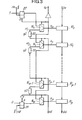
- Each of the registers 10 1 .... 10 p is associated with a sub-assembly comprising a flip-flop 12 1 .... 12p of RS type. all the scales being in cascade.
- Each subset provides a logic signal acting on the associated register and indicative of the free or occupied state of the register. This logic signal is produced as a function of the logic output signals of the preceding (or upstream) subset. of the next subset (or downstream). and the subset itself. the two end sub-assemblies naturally requiring a slightly different mounting.
- Figure 1 also carries. in parentheses. the abbreviations usually used on components of Anglo-Saxon origin.
- registers 10 1 to 10 p read the information in response to successive logic signals emitted by the corresponding subsets.
- the invention aims to provide a queue of the type defined above. but with fast operation and almost independent of the degree of filling of the queue. remaining however of a simple realization.
- the invention proposes in particular a queue in which the registers are of the type with locking in a transparent state and a locked state and each sub-assembly comprises a receiving switch. on its signal inputs. logic signals representative of the state of the upstream and downstream and transmitting subsets. on its output linked to the associated register. one of the two logic input signals. said output providing a signal representative of the state of said sub-assembly, the position of the switch being damaged by the logic level of the output signal of said switch.
- the registers implemented by the invention can be of the known type. for example can be constituted by registers F100-150 of the company FAIRCHILD.
- the data applied to the input appear instantly on the output when a command input is at a first logic level.
- the data applied to the entry of the register immediately before the transition remains applied to the exit-Thanks to the use of such registers.
- the register chain does not slow down the transit of data along the cascade when the registers are in the transparent state.
- control logic chain is intended to generate only. during the write operation. status logic signals which follow the progress of the information through the data registers until this information reaches the last empty register preceding a busy register.
- each switch is constituted by a 2 to 1 multiplexer.
- the output of the multiplexer directly controls the state of the associated register.
- each multiplexer will have an input connected to the output of the multiplexer of the previous stage, an input linked to the output of the next stage and a control input linked to its own output, the associated register being transparent when it receives a multiplexer output logic zero, which reflects the state of the input connected to the previous multiplexer when the control input receives a zero and reflects the state of the input connected to the next multiplexer when the control input receives a 1.
- each multiplexer chain In order for the multiplexer chain to function properly, it will generally be necessary to delay the transmission of information from each multiplexer to the previous one. To do this, simply apply the output of each multiplexer to the previous one via a delay element.
- This delay element will be such that the sum of the delay which it provides and the time of crossing of the multiplexer is greater than the switching time of the multiplexer.
- the queue can be supplemented by status indication outputs taken from the switches of at least some of the floors. On each of these outputs can be interposed a logical filtering cell intended to eliminate the transients caused by the descent or the ascent of the information.
- FIG. 2 schematically shows the mode of control by multiplexer on three successive registers
- FIG. 3 on which appear the control sub-assemblies of the first and last registers, whose structure is particular.
- the switch 16 i associated with the register 10 i constituted by a 2-to-1 multiplexer.
- the evolution of the switch 16 j is governed by three sources of information, its present state, the state of the stage above 16 i-1 , the state of the stage below 16 i + 1 . But, at a given moment, only two of these sources are decisive.
- the action of the switch 16 i is only determined by the state of the stage i i-1 .
- the read requests are materialized by rising edges applied to the input H1 and, when the queue is not empty, the first accessible data is available on the output DS. Activation of the H1 input also destroys this information, which is replaced by the content of the register immediately above 10 p-1 if it was not empty.
- each of the lines shows the appearance of the signals which appear at the point of the block diagram of Figure 3 which is designated by the same reference rence.
- the queue is four stages, that is to say has four registers 10 0 , 10 1 , 10 2 and 10 3 .
- a write order is materialized at time t 0 by a rising edge on the input He. This rising edge causes, at the end of time ⁇ , the rise of the writing flip-flop 22 (line BE). If we assume the register 10 0 empty. therefore transparent, the output at 0 is initially at 0. At the end of the time q 1 for crossing the multiplexer 16 0 , the output at 0 goes to 1 and causes the multiplexer 16 0 to switch again, at the end of the switching time q 0 . Indeed, the signal a 1 , and therefore the signal a ' 1 , is zero if the register 10 1 is empty.
- Figure 4 shows that the time for information to descend by stage is equal to q 1 , while the time for ascent of "hole" information, ie the existence downstream of an empty information register, is q 1 + q 2 .
- the queue the basic structure of which is shown in Figure 3, must be provided with status indicators if information about the content of the queue is to be available.
- the non-full or non-empty states of the queue are indicated, as in a queue in a conventional constitution register, by signals Ve and VI respectively taken from the output of the first multiplexer and from the output of the last multiplexer.
- Ve 0 means that the first register 10 0 is locked and that no writing can therefore be initiated.
- VI 1 indicates that information is available in the last register 10.
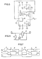
- the queue can advantageously be completed by elements indicating the intermediate filling states. Such elements are shown schematically in Figure 5.
- registers 10 0 , 10 i and 10 p as well as inputs and outputs. In principle, it is sufficient to determine that the queue is at least filled up to the level of register i, to verify that the corresponding signal a is at level 1. The information can then be taken from intermediate outputs 26 1 ,. .. 26 i , 26 p-1 . But this indication is not certain as a result of the transients caused by the progression of information and holes. This defect can be eliminated by interposing, on each of the outputs 26, a logic filtering cell 28 intended to make the positive or negative pulses having a duration less than a determined value disappear.
- the filter cell 28 can have the constitution shown in Figure 6 and include a rocker 30 interposed on the signal path to the output 32 i .
- the clock input of the flip-flop 30 receives an order prepared by an EXCLUSIVE OR gate 34, the inputs of which are connected one to the output 32 i , the other to the input via a line at delay r.
- the gate 34 detects a difference between the delayed input signal of T and the output signal, it activates the clock input of the flip-flop 30 which captures the current state of 26 i : we see on the timing diagram of Figure 6, where the lines indicate the shape of the signals at the locations designated by the same letter in Figure 6, that any pulse of duration shorter than ⁇ , for example those designated by 36, does not cause any change of state of flip-flop 30, the switches being caused only by signals representative of a real change in filling of the queue, as indicated at times t 1 .
Landscapes
- Engineering & Computer Science (AREA)
- Theoretical Computer Science (AREA)
- Physics & Mathematics (AREA)
- General Engineering & Computer Science (AREA)
- General Physics & Mathematics (AREA)
- Data Exchanges In Wide-Area Networks (AREA)
- Communication Control (AREA)
Applications Claiming Priority (2)
| Application Number | Priority Date | Filing Date | Title |
|---|---|---|---|
| FR8315510A FR2552916B1 (fr) | 1983-09-29 | 1983-09-29 | File d'attente asynchrone a empilement de registres |
| FR8315510 | 1983-09-29 |
Publications (2)
| Publication Number | Publication Date |
|---|---|
| EP0146418A1 true EP0146418A1 (de) | 1985-06-26 |
| EP0146418B1 EP0146418B1 (de) | 1988-01-07 |
Family
ID=9292660
Family Applications (1)
| Application Number | Title | Priority Date | Filing Date |
|---|---|---|---|
| EP84401952A Expired EP0146418B1 (de) | 1983-09-29 | 1984-09-28 | Asynchroner Puffer mit gestapelten Registern |
Country Status (6)
| Country | Link |
|---|---|
| US (1) | US4819201A (de) |
| EP (1) | EP0146418B1 (de) |
| JP (1) | JPS6093556A (de) |
| CA (1) | CA1216371A (de) |
| DE (1) | DE3468558D1 (de) |
| FR (1) | FR2552916B1 (de) |
Cited By (1)
| Publication number | Priority date | Publication date | Assignee | Title |
|---|---|---|---|---|
| EP0416513A3 (en) * | 1989-09-04 | 1992-08-19 | Matsushita Electric Industrial Co., Ltd. | Fifo memory device |
Families Citing this family (20)
| Publication number | Priority date | Publication date | Assignee | Title |
|---|---|---|---|---|
| NL8502023A (nl) * | 1985-07-15 | 1987-02-02 | Philips Nv | Werkwijze voor het schakelen van tijdsloten in een tdm-signaal en inrichting voor het uitvoeren van de werkwijze. |
| US4672646A (en) * | 1986-09-16 | 1987-06-09 | Hewlett-Packard Company | Direct-injection FIFO shift register |
| US5255238A (en) * | 1988-09-08 | 1993-10-19 | Hitachi, Ltd. | First-in first-out semiconductor memory device |
| JP3085311B2 (ja) * | 1990-05-25 | 2000-09-04 | 日本電信電話株式会社 | Fifoバッファ |
| JP2734465B2 (ja) * | 1991-04-10 | 1998-03-30 | 三菱電機株式会社 | ネットワーク用入出力装置 |
| US5255239A (en) * | 1991-08-13 | 1993-10-19 | Cypress Semiconductor Corporation | Bidirectional first-in-first-out memory device with transparent and user-testable capabilities |
| DK192491D0 (da) * | 1991-11-26 | 1991-11-26 | Stig Magnar George B Harlequin | Anordning til parallel-kobling af datamater |
| US5504913A (en) * | 1992-05-14 | 1996-04-02 | Apple Computer, Inc. | Queue memory with self-handling addressing and underflow |
| US5838933A (en) * | 1993-10-21 | 1998-11-17 | Sun Microsystems, Inc. | Control circuit and method for a first-in first-out data pipeline |
| US5680644A (en) * | 1994-10-31 | 1997-10-21 | Digital Equipment Corporation | Low delay means of communicating between systems on different clocks |
| SE515563C2 (sv) * | 1995-01-11 | 2001-08-27 | Ericsson Telefon Ab L M | Dataöverföringssystem |
| SE503914C2 (sv) * | 1995-01-27 | 1996-09-30 | Ericsson Telefon Ab L M | Dataöverföringssystem |
| US6091426A (en) * | 1995-04-07 | 2000-07-18 | Intel Corporation | Integrating data scaling and buffering functions to minimize memory requirement |
| US5937177A (en) * | 1996-10-01 | 1999-08-10 | Sun Microsystems, Inc. | Control structure for a high-speed asynchronous pipeline |
| US5920899A (en) * | 1997-09-02 | 1999-07-06 | Acorn Networks, Inc. | Asynchronous pipeline whose stages generate output request before latching data |
| US6507877B1 (en) | 1999-09-03 | 2003-01-14 | Whamtech, Inc. | Asynchronous concurrent dual-stream FIFO |
| US6700825B1 (en) | 2000-09-29 | 2004-03-02 | Sun Microsystems, Inc. | Implementation of a multi-dimensional, low latency, first-in first-out (FIFO) buffer |
| US6420907B1 (en) | 2000-09-29 | 2002-07-16 | Sun Microsystems, Inc. | Method and apparatus for asynchronously controlling state information within a circuit |
| US8480398B1 (en) * | 2007-12-17 | 2013-07-09 | Tamer Yunten | Yunten model computer system and lab kit for education |
| US9411722B2 (en) | 2013-03-04 | 2016-08-09 | Sandisk Technologies Llc | Asynchronous FIFO buffer for memory access |
Citations (3)
| Publication number | Priority date | Publication date | Assignee | Title |
|---|---|---|---|---|
| US3378776A (en) * | 1964-10-09 | 1968-04-16 | Stanford Research Inst | Data shifting logic system with data and control signals advancing through the system in opposite directions |
| US3953838A (en) * | 1974-12-30 | 1976-04-27 | Burroughs Corporation | FIFO Buffer register memory utilizing a one-shot data transfer system |
| GB2009984A (en) * | 1977-12-12 | 1979-06-20 | Philips Nv | Data buffer memory |
Family Cites Families (8)
| Publication number | Priority date | Publication date | Assignee | Title |
|---|---|---|---|---|
| US3988717A (en) * | 1975-08-06 | 1976-10-26 | Litton Systems, Inc. | General purpose computer or logic chip and system |
| US4157587A (en) * | 1977-12-22 | 1979-06-05 | Honeywell Information Systems Inc. | High speed buffer memory system with word prefetch |
| JPS5680743U (de) * | 1979-11-28 | 1981-06-30 | ||
| US4369510A (en) * | 1980-07-25 | 1983-01-18 | Honeywell Information Systems Inc. | Soft error rewrite control system |
| US4486854A (en) * | 1981-10-15 | 1984-12-04 | Codex Corporation | First-in, first-out memory system |
| US4558429A (en) * | 1981-12-17 | 1985-12-10 | Honeywell Information Systems Inc. | Pause apparatus for a memory controller with interleaved queuing apparatus |
| JPS5936390A (ja) * | 1982-08-24 | 1984-02-28 | Nippon Telegr & Teleph Corp <Ntt> | レジスタ回路 |
| US4642797A (en) * | 1983-11-10 | 1987-02-10 | Monolithic Memories, Inc. | High speed first-in-first-out memory |
-
1983
- 1983-09-29 FR FR8315510A patent/FR2552916B1/fr not_active Expired
-
1984
- 1984-09-28 DE DE8484401952T patent/DE3468558D1/de not_active Expired
- 1984-09-28 EP EP84401952A patent/EP0146418B1/de not_active Expired
- 1984-09-28 JP JP59203921A patent/JPS6093556A/ja active Granted
- 1984-09-28 CA CA000464349A patent/CA1216371A/en not_active Expired
-
1987
- 1987-07-27 US US07/077,999 patent/US4819201A/en not_active Expired - Lifetime
Patent Citations (3)
| Publication number | Priority date | Publication date | Assignee | Title |
|---|---|---|---|---|
| US3378776A (en) * | 1964-10-09 | 1968-04-16 | Stanford Research Inst | Data shifting logic system with data and control signals advancing through the system in opposite directions |
| US3953838A (en) * | 1974-12-30 | 1976-04-27 | Burroughs Corporation | FIFO Buffer register memory utilizing a one-shot data transfer system |
| GB2009984A (en) * | 1977-12-12 | 1979-06-20 | Philips Nv | Data buffer memory |
Cited By (2)
| Publication number | Priority date | Publication date | Assignee | Title |
|---|---|---|---|---|
| EP0416513A3 (en) * | 1989-09-04 | 1992-08-19 | Matsushita Electric Industrial Co., Ltd. | Fifo memory device |
| US5157633A (en) * | 1989-09-04 | 1992-10-20 | Matsushita Electric Industrial Co., Ltd. | Fifo memory device |
Also Published As
| Publication number | Publication date |
|---|---|
| JPS6093556A (ja) | 1985-05-25 |
| FR2552916B1 (fr) | 1988-06-10 |
| FR2552916A1 (fr) | 1985-04-05 |
| DE3468558D1 (en) | 1988-02-11 |
| JPH0554138B2 (de) | 1993-08-11 |
| CA1216371A (en) | 1987-01-06 |
| US4819201A (en) | 1989-04-04 |
| EP0146418B1 (de) | 1988-01-07 |
Similar Documents
| Publication | Publication Date | Title |
|---|---|---|
| EP0146418B1 (de) | Asynchroner Puffer mit gestapelten Registern | |
| EP0076196B1 (de) | System zur Konfliktlösung von Zugriffsanforderungen von mehreren Prozessoren für gemeinsame Betriebsmittel, mit Hilfe einer Sammelschiene | |
| EP0109898A1 (de) | Warteschlangen organisierter temporärer Datenspeicher | |
| CA1240061A (fr) | Dispositifs de synchronisation de trame | |
| FR2591776A1 (fr) | Circuit de resynchronisation de signaux pulses, en particulier pour peripheriques de microprocesseurs | |
| FR2487076A1 (fr) | Dispositif pour le controle d'un circuit comportant des elements a fonctionnement numerique et a fonctionnement combinatoire | |
| FR2849228A1 (fr) | Dispositif de transfert de donnees entre deux sous-systemes asynchrones disposant d'une memoire tampon | |
| EP0046110B1 (de) | Schaltung zur Erlangung eines Zeit-Abstands-Histogramms aufeinanderfolgender Ereignisse | |
| EP0025731A1 (de) | Auswahlschaltung für asynchronen Anforderungen in einem Datenverarbeitungssystem | |
| FR3134462A1 (fr) | Procédé de transfert de données entre un premier domaine numérique et un deuxième domaine numérique, et système sur puce correspondant. | |
| EP0707260B1 (de) | Asynchrone Speicheranordnung mit seriellem Zugriff und entsprechendes Speicher- und Leseverfahren | |
| EP0011701A1 (de) | Auswahlsystem für Vorrangsschnittstellen und Datenübertragungssteuereinrichtung mit solchem Auswahlsystem | |
| FR2588088A1 (fr) | Dispositif de generation de signaux de temps | |
| EP0889481B1 (de) | Verbesserungen von Speicherschaltungen mit sequentiellem Zugriff | |
| EP0344052B1 (de) | Modularer Speicher | |
| FR2710804A1 (fr) | Dispositif numérique de connexion d'une pluralité de stations de travail sur un réseau local en anneau. | |
| EP0082765B1 (de) | Managementsvorrichtung eines gemeinsam benutzten Speichers mit mehreren Prozessoren | |
| EP0033673B1 (de) | Regenerierungsverfahren für ein MOS-Speichersystem und entsprechende Steuerschaltung | |
| CA1092245A (fr) | Dispositif de synchronisation "trame" | |
| EP0640910B1 (de) | Verfahren zur Steuerung einer FIFO-Schaltung und Einrichtung zu seiner Durchführung | |
| EP0196255B1 (de) | Verfahren zur Erzeugung eines synchronen Taktsignals von einem einfachen oder doppelten dichtheitskodiertem Signal und Anordnung zur Durchführung des Verfahrens | |
| EP0658838A1 (de) | Frequenzsynthetisierer | |
| EP1748355A1 (de) | Vorrichtung zur unidirektionalen Interface-Verbindung des FIFO-Typs zwischen einem Master-Block und einem Slave-Block, sowie entsprechender Master- und Slave-Block | |
| EP1739567A1 (de) | Vorrichtung zur asynchronen Arbitration und Mikrokontroller, der eine solche Arbitrationsvorrichtung umfasst | |
| EP0717349B1 (de) | Anordnung zur Verwaltung eines FIFO-Speichers |
Legal Events
| Date | Code | Title | Description |
|---|---|---|---|
| PUAI | Public reference made under article 153(3) epc to a published international application that has entered the european phase |
Free format text: ORIGINAL CODE: 0009012 |
|
| AK | Designated contracting states |
Designated state(s): BE CH DE GB IT LI NL SE |
|
| 17P | Request for examination filed |
Effective date: 19850704 |
|
| 17Q | First examination report despatched |
Effective date: 19870218 |
|
| GRAA | (expected) grant |
Free format text: ORIGINAL CODE: 0009210 |
|
| AK | Designated contracting states |
Kind code of ref document: B1 Designated state(s): BE CH DE GB IT LI NL SE |
|
| ITF | It: translation for a ep patent filed | ||
| REF | Corresponds to: |
Ref document number: 3468558 Country of ref document: DE Date of ref document: 19880211 |
|
| GBT | Gb: translation of ep patent filed (gb section 77(6)(a)/1977) | ||
| PLBE | No opposition filed within time limit |
Free format text: ORIGINAL CODE: 0009261 |
|
| STAA | Information on the status of an ep patent application or granted ep patent |
Free format text: STATUS: NO OPPOSITION FILED WITHIN TIME LIMIT |
|
| 26N | No opposition filed | ||
| ITTA | It: last paid annual fee | ||
| EAL | Se: european patent in force in sweden |
Ref document number: 84401952.1 |
|
| REG | Reference to a national code |
Ref country code: GB Ref legal event code: IF02 |
|
| PGFP | Annual fee paid to national office [announced via postgrant information from national office to epo] |
Ref country code: SE Payment date: 20030825 Year of fee payment: 20 Ref country code: NL Payment date: 20030825 Year of fee payment: 20 Ref country code: BE Payment date: 20030825 Year of fee payment: 20 |
|
| PGFP | Annual fee paid to national office [announced via postgrant information from national office to epo] |
Ref country code: CH Payment date: 20030826 Year of fee payment: 20 |
|
| PGFP | Annual fee paid to national office [announced via postgrant information from national office to epo] |
Ref country code: GB Payment date: 20030829 Year of fee payment: 20 |
|
| PGFP | Annual fee paid to national office [announced via postgrant information from national office to epo] |
Ref country code: DE Payment date: 20030909 Year of fee payment: 20 |
|
| PG25 | Lapsed in a contracting state [announced via postgrant information from national office to epo] |
Ref country code: LI Free format text: LAPSE BECAUSE OF EXPIRATION OF PROTECTION Effective date: 20040927 Ref country code: GB Free format text: LAPSE BECAUSE OF EXPIRATION OF PROTECTION Effective date: 20040927 Ref country code: CH Free format text: LAPSE BECAUSE OF EXPIRATION OF PROTECTION Effective date: 20040927 |
|
| PG25 | Lapsed in a contracting state [announced via postgrant information from national office to epo] |
Ref country code: NL Free format text: LAPSE BECAUSE OF EXPIRATION OF PROTECTION Effective date: 20040928 |
|
| BE20 | Be: patent expired |
Owner name: *SERVEL MICHEL Effective date: 20040928 Owner name: *THOMAS ALAIN Effective date: 20040928 |
|
| REG | Reference to a national code |
Ref country code: GB Ref legal event code: PE20 |
|
| REG | Reference to a national code |
Ref country code: CH Ref legal event code: PL |
|
| EUG | Se: european patent has lapsed | ||
| REG | Reference to a national code |
Ref country code: SE Ref legal event code: EUG |
|
| NLV7 | Nl: ceased due to reaching the maximum lifetime of a patent |
Effective date: 20040928 |