EP0146513A2 - Source de courant pour le soudage à l'arc - Google Patents
Source de courant pour le soudage à l'arc Download PDFInfo
- Publication number
- EP0146513A2 EP0146513A2 EP84850364A EP84850364A EP0146513A2 EP 0146513 A2 EP0146513 A2 EP 0146513A2 EP 84850364 A EP84850364 A EP 84850364A EP 84850364 A EP84850364 A EP 84850364A EP 0146513 A2 EP0146513 A2 EP 0146513A2
- Authority
- EP
- European Patent Office
- Prior art keywords
- voltage
- welding
- inverters
- current source
- inverter
- Prior art date
- Legal status (The legal status is an assumption and is not a legal conclusion. Google has not performed a legal analysis and makes no representation as to the accuracy of the status listed.)
- Withdrawn
Links
Images
Classifications
-
- B—PERFORMING OPERATIONS; TRANSPORTING
- B23—MACHINE TOOLS; METAL-WORKING NOT OTHERWISE PROVIDED FOR
- B23K—SOLDERING OR UNSOLDERING; WELDING; CLADDING OR PLATING BY SOLDERING OR WELDING; CUTTING BY APPLYING HEAT LOCALLY, e.g. FLAME CUTTING; WORKING BY LASER BEAM
- B23K9/00—Arc welding or cutting
- B23K9/10—Other electric circuits therefor; Protective circuits; Remote controls
- B23K9/1006—Power supply
-
- B—PERFORMING OPERATIONS; TRANSPORTING
- B23—MACHINE TOOLS; METAL-WORKING NOT OTHERWISE PROVIDED FOR
- B23K—SOLDERING OR UNSOLDERING; WELDING; CLADDING OR PLATING BY SOLDERING OR WELDING; CUTTING BY APPLYING HEAT LOCALLY, e.g. FLAME CUTTING; WORKING BY LASER BEAM
- B23K9/00—Arc welding or cutting
- B23K9/06—Arrangements or circuits for starting the arc, e.g. by generating ignition voltage, or for stabilising the arc
-
- H—ELECTRICITY
- H02—GENERATION; CONVERSION OR DISTRIBUTION OF ELECTRIC POWER
- H02J—ELECTRIC POWER NETWORKS; CIRCUIT ARRANGEMENTS OR SYSTEMS FOR SUPPLYING OR DISTRIBUTING ELECTRIC POWER; SYSTEMS FOR STORING ELECTRIC ENERGY
- H02J1/00—Circuit arrangements for DC mains or DC distribution networks
- H02J1/10—Parallel operation of DC sources
- H02J1/102—Parallel operation of DC sources being switching converters
-
- H—ELECTRICITY
- H02—GENERATION; CONVERSION OR DISTRIBUTION OF ELECTRIC POWER
- H02J—ELECTRIC POWER NETWORKS; CIRCUIT ARRANGEMENTS OR SYSTEMS FOR SUPPLYING OR DISTRIBUTING ELECTRIC POWER; SYSTEMS FOR STORING ELECTRIC ENERGY
- H02J1/00—Circuit arrangements for DC mains or DC distribution networks
- H02J1/10—Parallel operation of DC sources
- H02J1/108—Parallel operation of DC sources having arrangements for blocking reverse current flow, e.g. using diodes
Definitions
- the invention relates to a welding current source for arc welding with a rectifier that can be connected to an AC network, a parallel circuit connected to its DC terminals, consisting of a smoothing capacitor device and an inverter device for converting the DC voltage into an AC voltage, the frequency of which is significantly higher than the mains frequency, whereby the inverter device is equipped with semiconductor elements which are controlled by a control unit and is equipped with a transformer device for the galvanic isolation of the input of the inverter device from its output, to which, after an optional series connection of a rectifier, a welding point formed from a workpiece and a welding electrode can be connected.
- Welding current sources are usually equipped with a transformer for reducing the mains voltage to the lower welding voltage. Thanks to the use of a significantly higher frequency, the size of the transformer is significantly reduced compared to the size of a transformer of the same power for the mains frequency. Frequencies of at least 0.5 kHz are understood here as significantly higher frequencies. It is particularly expedient to choose a frequency which is more than 15 kHz and is therefore above the audibility threshold. The higher frequency allows a faster regulation of the welding parameters, in particular the welding current and the welding voltage, compared to the mains frequency. Welding current sources of this type are known for example from US 4 159 409 and GB 2 046 535.
- controllable semiconductor elements for higher frequencies are expensive and in some respects have poorer operating values than corresponding semiconductor elements for normal network frequencies. In particular, these semiconductor elements have poorer characteristic values, which undermines their overload capacity through compensating processes, e.g. rapid current and voltage changes. Such semiconductor elements for normal line voltages are particularly expensive.
- mains voltage of 380 V the smoothed DC voltage is approximately 530 V. Since the dimensioning of the semiconductor elements also has to take into account the fluctuation in the mains voltage and compensation processes, it is necessary to design the semiconductor elements for approximately 600 V at a mains voltage of 380 V and for approximately 800 V at a mains voltage of 500 V.
- the present invention has therefore set itself the task of a cheap welding power source with change richter to create, in which these less expensive semiconductor elements can be used at common line voltages.
- the solution to this problem is that the inverter device consists of two or more inverters, the inputs of which are connected in series, and that the smoothing capacitor device serves as a voltage divider that consists of two or more capacitors connected in series, with connections arranged between the capacitors with corresponding connections are connected between the inverters connected in series.
- Each inverter is therefore only a part of the total voltage and it is therefore possible to use semiconductor elements which are only to be designed for these partial voltages.
- the inputs of two inverters of the same type are connected in series and control devices of the two inverters are provided for controlling the semiconductor elements for alternately generating voltage pulses at the outputs of the two inverters, a circuit consisting of between each output and the welding point a series connection of rectifier and welding inductor and one with the Welding inductor interacting free-wheeling diode is switched on.
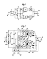
- a rectifier 1 is connected to a single-phase network 2.
- Two to a line 3 in series g esch ALTENE inverters 4, 5 are connected to lines 6, 7 to the rectifier. 1
- the inverters are equipped with controllable semiconductor elements. Inverter circuits of this type are generally known.
- the semiconductor elements can be thyristors and transistors.
- the frequency of the AC voltage output by the inverters 4, 5 is preferably 15 kHz or higher.
- the AC voltage is rectified in the corresponding rectifier 13, 14 and fed to a welding point consisting of electrode 15 and workpiece 16.
- the resistors 10, 11 are the same size and the voltage across each of the two inverters is therefore also approximately the same size. Slight deviations from these voltage values occur due to the charging and discharging of the capacitors taking place in time with the inverter frequency.
- FIG. 2 shows a three-phase rectifier 17 which is connected to a three-phase network 18.
- Two smoothing capacitors 21, 22 connected in series and two inverters 23, 24 connected in series with their inputs 25, 26, 27, 28 are connected to the output 19, 20 of the rectifier.
- the inputs 26, 27 are connected by a terminal 29 which is connected to a terminal 30 of the connecting line of the two capacitors 21, 22.
- the outputs 31, 32, 33, 34 of the inverters are connected in series with one diode 35, 36 and one welding inductor 37, 38 each.
- a free-wheeling diode 39, 40 for each output takes over the welding current when the energy flow is interrupted by the inverter.
- the two output circuits 35, 37, 39 and 36, 38, 40 are connected in parallel and connected to a welding electrode 41 and a workpiece 42.
- the circuit of the two inverters 23, 24 is identical and therefore only one of the two inverters is described in more detail.
- the parts of the inverters 23, 24 are provided with the same reference symbols.
- the inverter 23 is an asymmetrical half-bridge inverter. Two in parallel Circles each contain a diode 43, 44 and a semiconductor element 46, 47 which can be controlled by a control device 45.
- MOS field effect transistors also called Mosfet for short, are used as semiconductor elements which, in contrast to the normal bipolar transistors, are controlled practically without power will.
- the mosfet has a positive temperature coefficient, i.e. its resistance increases with increasing temperature.
- the Mosfet can therefore be connected in parallel without special switching elements or auxiliary circuits, the current being distributed over the Mosfets connected in parallel in the ratio of the resistances. Due to the positive temperature coefficient, overloads in the Mosfet cannot cause an uncontrollable increase in current, since local heating in the overloaded area of the Mosfet leads to a corresponding decrease in current.
- the Mosfet thus has several advantages over the bipolar transistor.
- a disadvantage is the low dielectric strength.
- Mosfets with blocking voltages up to 800 V are currently available.
- these mosfets are expensive, especially for the high currents for which welding current sources have to be dimensioned. It is therefore understandable that the use of cheap mosfets with low dielectric strength is desirable.
- the primary winding 49 of a transformer 48 is connected between the two MOSFETs.
- Resistors 51, 52 are connected between one connection of transformer 48 and the two connections 25, 29.
- the secondary winding 50 of the transformer is connected directly to the output 31, 32 of the inverter.
- the resistors 51, 52 in the two inverters act in the same way as described above for the resistors 10, 11 in FIG. 1.
- the DC voltage of the rectifier 17 is divided into two equal partial voltages between the terminals 25, 29 and 29, 28 by the two pairs of resistors 51, 52, which have the same resistance.
- the potential of the connection points 29, 30 is therefore theoretically between the two potentials of the rectifier outputs 19, 20.
- slight fluctuations in the potential of the connection points 29, 30 are caused, for example, by different pulse lengths of the control signals to the Mosfets and by different charge and discharge currents of the capacitors .
- the Mosfets of the two inverters 23, 24 are thus only exposed to half the operating DC voltage occurring between the terminals 25, 29 and 29, 28 plus a small surcharge for the potential fluctuations occurring in the terminal 29.
- the potential of the terminal 29 can deviate greatly from its operating value, as a result of which the voltage at one of the inverters can be increased such that the Mosfets are exposed to a destructive surge.
- the occurrence of such an overvoltage on the mosfet is avoided with the help of a monitoring circuit.
- the voltage of the capacitor 22 is compared in a comparator 53 with a voltage set by means of an actuator 54. If the difference between the capacitor voltage and the set voltage exceeds a certain value, the comparator 53 emits a signal to the control device, which immediately blocks the MOSFET 46, 47 via the control lines 55.
- each Mosfet is therefore only loaded with about a quarter of the DC voltage between the output terminals 19, 20 as long as the capacitors are free of defects.
- the voltage between the terminals 19, 20 is divided between the two capacitors in the inverse proportion to their capacitance. Since the mass-produced capacitors available on the market have capacitance values that can deviate significantly from their nominal value within the permissible tolerances, it can be expected that the inverters will not be at the same instant, as intended, but at very different partial voltages. After a short time, however, the partial voltages will set to a value which is determined by the resistors 51, 52 in the inverters 23, 24. The surge voltages at the moment of switching on can damage the Mosfets. It would now be possible to select suitable capacitors with the same capacitance values, but this incurs additional costs.
- the voltage of the capacitor 22 is running from the comparator If an overvoltage is monitored on one of the two capacitors 21, 22, the difference between the voltage of the capacitor 22 and the voltage set on the actuator 54 of the comparator exceeds a predetermined value. A corresponding output signal from the comparator 53 to the control unit 45 leads to an immediate blocking of the Mosfets.
- the voltage across a MOSFET can therefore in the worst case - if, for example, one of the two capacitors 21, 22 is defective and short-circuited - make up at most half the voltage between the terminals 19, 20, since, as assumed above, the resistors 51, 52 are the same are big.
- a voltage corresponding to the welding current is tapped at a shunt 56, which voltage is fed together with the welding voltage via lines 51, 58, 59 to the control device 45 common to both inverters.
- An actuator 60 is provided on the control device for setting the setpoint value of welding current and / or welding voltage. In contrast to the illustration shown here, it is also conceivable to provide each inverter with its own control unit.
- the two inverters 23, 24 are expediently operated by the control device as pulse-width-modulated inverters in push-pull mode.
- the inverters emit alternating voltage pulses of a certain length at their outputs 31, 32 and 33, 34. If the inverters are loaded in this way, it has proven to be advantageous to use the inverters 23, 24 with their rectifiers 35, 36, their welding inductors 37, 38 and each to connect their freewheeling diode 39, 40 before the two inverters are connected in parallel and connected to the common welding point 41, 42.
Landscapes
- Engineering & Computer Science (AREA)
- Physics & Mathematics (AREA)
- Plasma & Fusion (AREA)
- Mechanical Engineering (AREA)
- Power Engineering (AREA)
- Inverter Devices (AREA)
- Arc Welding Control (AREA)
- Arc Welding In General (AREA)
Applications Claiming Priority (2)
| Application Number | Priority Date | Filing Date | Title |
|---|---|---|---|
| SE8306550 | 1983-11-28 | ||
| SE8306550A SE438109B (sv) | 1983-11-28 | 1983-11-28 | Stromkella for ljusbagsvetsning |
Publications (2)
| Publication Number | Publication Date |
|---|---|
| EP0146513A2 true EP0146513A2 (fr) | 1985-06-26 |
| EP0146513A3 EP0146513A3 (fr) | 1987-12-02 |
Family
ID=20353488
Family Applications (1)
| Application Number | Title | Priority Date | Filing Date |
|---|---|---|---|
| EP84850364A Withdrawn EP0146513A3 (fr) | 1983-11-28 | 1984-11-26 | Source de courant pour le soudage à l'arc |
Country Status (7)
| Country | Link |
|---|---|
| US (1) | US4564742A (fr) |
| EP (1) | EP0146513A3 (fr) |
| JP (1) | JPS60133978A (fr) |
| DK (1) | DK149664B (fr) |
| FI (1) | FI75513C (fr) |
| NO (1) | NO163395C (fr) |
| SE (1) | SE438109B (fr) |
Cited By (3)
| Publication number | Priority date | Publication date | Assignee | Title |
|---|---|---|---|---|
| GB2225909A (en) * | 1988-11-17 | 1990-06-13 | Honda Motor Co Ltd | DC resistance welding apparatus |
| US5196668A (en) * | 1988-11-17 | 1993-03-23 | Honda Giken Kogyo Kabushiki Kaisha | DC resistance welding apparatus |
| US5229567A (en) * | 1988-11-17 | 1993-07-20 | Honda Giken Kogyo Kabushiki Kaisha | Switching control system for controlling an inverter of a spot resistance welding apparatus |
Families Citing this family (31)
| Publication number | Priority date | Publication date | Assignee | Title |
|---|---|---|---|---|
| US4763237A (en) * | 1986-10-17 | 1988-08-09 | Wieczorek John P | DC/AC/DC Power conversion system including parallel transformers |
| DE3803447C1 (fr) * | 1988-02-05 | 1989-05-24 | B & V Beschichten Und Verbinden Gmbh, 6800 Mannheim, De | |
| DE3804387C1 (en) * | 1988-02-12 | 1989-08-24 | B & V Beschichten Und Verbinden Gmbh, 6800 Mannheim, De | Arc welding device having an extended drive range |
| US4916599A (en) * | 1989-03-29 | 1990-04-10 | Hyperpower, Inc. | Switching power supply |
| DE59000536D1 (de) * | 1989-07-26 | 1993-01-14 | Elektro Werk Muendersbach Gmbh | Schweiss- oder plasmaschneidgeraet mit stabilisierter zwischenkreisspannung. |
| JP3003159B2 (ja) * | 1989-12-28 | 2000-01-24 | 株式会社ダイヘン | 交流アーク溶接用電源 |
| DE59003559D1 (de) * | 1990-11-27 | 1993-12-23 | Siemens Ag | Hochfrequenz-Röntgengenerator. |
| US5319533A (en) * | 1992-01-17 | 1994-06-07 | Miller Electric Mfg. Co. | Power selection and protection circuit responsive to an input voltage for providing series or parallel connected inverters |
| US5351175A (en) * | 1993-02-05 | 1994-09-27 | The Lincoln Electric Company | Inverter power supply for welding |
| US5601741A (en) * | 1994-11-18 | 1997-02-11 | Illinois Tool Works, Inc. | Method and apparatus for receiving a universal input voltage in a welding power source |
| JP3302581B2 (ja) * | 1996-11-29 | 2002-07-15 | 日立ビアメカニクス株式会社 | アーク溶接用電源 |
| JP3231705B2 (ja) * | 1998-07-08 | 2001-11-26 | 株式会社三社電機製作所 | アーク加工用電源装置 |
| US6023037A (en) | 1998-11-05 | 2000-02-08 | Lincoln Global, Inc. | Electric ARC welder and plasma cutter |
| US6111216A (en) * | 1999-01-19 | 2000-08-29 | Lincoln Global, Inc. | High current welding power supply |
| US6291798B1 (en) * | 1999-09-27 | 2001-09-18 | Lincoln Global, Inc. | Electric ARC welder with a plurality of power supplies |
| DE10001344A1 (de) * | 2000-01-14 | 2001-07-19 | Emhart Inc | Verfahren und Vorrichtung zum mehrstufigen Lichtbogenschweißen |
| US6268587B1 (en) * | 2000-02-22 | 2001-07-31 | Lincoln Global, Inc. | Current feedback device for electric arc welder |
| US6329636B1 (en) * | 2000-03-31 | 2001-12-11 | Illinois Tool Works Inc. | Method and apparatus for receiving a universal input voltage in a welding plasma or heating power source |
| US6713721B2 (en) * | 2001-09-19 | 2004-03-30 | Illinois Tool Works Inc. | Method of designing and manufacturing welding-type power supplies |
| US20040179923A1 (en) * | 2002-12-23 | 2004-09-16 | Lockheed Martin Corporation | Automated transportation mechanism for conveyence and positioning of test containers |
| US8269141B2 (en) * | 2004-07-13 | 2012-09-18 | Lincoln Global, Inc. | Power source for electric arc welding |
| US9956639B2 (en) | 2005-02-07 | 2018-05-01 | Lincoln Global, Inc | Modular power source for electric ARC welding and output chopper |
| US8581147B2 (en) * | 2005-03-24 | 2013-11-12 | Lincoln Global, Inc. | Three stage power source for electric ARC welding |
| US8785816B2 (en) * | 2004-07-13 | 2014-07-22 | Lincoln Global, Inc. | Three stage power source for electric arc welding |
| US9855620B2 (en) | 2005-02-07 | 2018-01-02 | Lincoln Global, Inc. | Welding system and method of welding |
| US9647555B2 (en) * | 2005-04-08 | 2017-05-09 | Lincoln Global, Inc. | Chopper output stage for arc welder power source |
| US9908199B2 (en) * | 2013-03-07 | 2018-03-06 | GM Global Technology Operations LLC | Programmable polarity module for DC resistance spot welding |
| US9539661B2 (en) | 2013-06-24 | 2017-01-10 | Illinois Tool Works Inc. | Welding power supply extended range system and method |
| US9584024B2 (en) | 2013-06-24 | 2017-02-28 | Illinois Tool Works Inc. | Metal working power supply converter system and method |
| US20180207741A1 (en) * | 2017-01-25 | 2018-07-26 | Lincoln Global, Inc. | Battery jump and charge system and method for a welder |
| US20200030904A1 (en) * | 2018-07-25 | 2020-01-30 | Illinois Tool Works Inc. | Systems and methods to mitigate audible noise in welding-type power supplies |
Family Cites Families (6)
| Publication number | Priority date | Publication date | Assignee | Title |
|---|---|---|---|---|
| US3728516A (en) * | 1970-10-16 | 1973-04-17 | A Daspit | Welding power source |
| US4062057A (en) * | 1977-04-15 | 1977-12-06 | The United States Of America As Represented By The Secretary Of The Navy | Regulated power supply having a series arrangement of inverters |
| NO790942L (no) * | 1978-04-12 | 1979-10-15 | Migatronic Svejsemask | Sveisemaskin. |
| US4276590A (en) * | 1979-04-30 | 1981-06-30 | The Perkin-Elmer Corporation | Current sharing modular power system |
| GB2064891B (en) * | 1979-11-20 | 1983-06-22 | Hirschmann F | Thyristor converter circuit for welding apparatus |
| US4503316A (en) * | 1981-08-13 | 1985-03-05 | Kabushiki Kaisha Kobe Seiko Sho | DC Welding power supply system |
-
1983
- 1983-11-28 SE SE8306550A patent/SE438109B/sv not_active IP Right Cessation
-
1984
- 1984-11-15 FI FI844488A patent/FI75513C/fi not_active IP Right Cessation
- 1984-11-19 US US06/672,720 patent/US4564742A/en not_active Expired - Fee Related
- 1984-11-22 DK DK555984A patent/DK149664B/da not_active Application Discontinuation
- 1984-11-26 EP EP84850364A patent/EP0146513A3/fr not_active Withdrawn
- 1984-11-26 JP JP59248253A patent/JPS60133978A/ja active Granted
- 1984-11-27 NO NO844724A patent/NO163395C/no unknown
Cited By (5)
| Publication number | Priority date | Publication date | Assignee | Title |
|---|---|---|---|---|
| GB2225909A (en) * | 1988-11-17 | 1990-06-13 | Honda Motor Co Ltd | DC resistance welding apparatus |
| US5120929A (en) * | 1988-11-17 | 1992-06-09 | Honda Giken Kogyo Kabushiki Kaisha | Dc resistance welding apparatus |
| US5196668A (en) * | 1988-11-17 | 1993-03-23 | Honda Giken Kogyo Kabushiki Kaisha | DC resistance welding apparatus |
| US5229567A (en) * | 1988-11-17 | 1993-07-20 | Honda Giken Kogyo Kabushiki Kaisha | Switching control system for controlling an inverter of a spot resistance welding apparatus |
| GB2225909B (en) * | 1988-11-17 | 1993-11-24 | Honda Motor Co Ltd | DC resistance welding apparatus |
Also Published As
| Publication number | Publication date |
|---|---|
| DK149664B (da) | 1986-09-01 |
| JPH0245952B2 (fr) | 1990-10-12 |
| FI75513C (fi) | 1988-07-11 |
| DK555984D0 (da) | 1984-11-22 |
| FI75513B (fi) | 1988-03-31 |
| NO844724L (no) | 1985-05-29 |
| FI844488A0 (fi) | 1984-11-15 |
| US4564742A (en) | 1986-01-14 |
| SE8306550D0 (sv) | 1983-11-28 |
| FI844488L (fi) | 1985-05-29 |
| JPS60133978A (ja) | 1985-07-17 |
| NO163395B (no) | 1990-02-12 |
| EP0146513A3 (fr) | 1987-12-02 |
| DK555984A (da) | 1985-05-29 |
| NO163395C (no) | 1990-05-23 |
| SE438109B (sv) | 1985-04-01 |
Similar Documents
| Publication | Publication Date | Title |
|---|---|---|
| EP0146513A2 (fr) | Source de courant pour le soudage à l'arc | |
| EP3280052B1 (fr) | Procede et dispositif de commande d'un circuit semi-conducteur de puissance commande par tension | |
| DE69712243T2 (de) | Universeller Leistungsmodul | |
| DE19702134A1 (de) | Schutzschaltung für Hochleistungs-Schalterbauteile | |
| DE69317194T2 (de) | Schaltnetzteil | |
| DE102008039593A1 (de) | Steuerschaltung für einen Generator, eine Generatorbaugruppe, und Verfahren zur Steuerung der Ausgangsspannung eines Generators | |
| DE69733679T2 (de) | Schaltnetzteil | |
| DE2524367A1 (de) | Schaltung zur umwandlung von wechselspannungen in eine gleichspannung konstanter groesse | |
| EP2945257B1 (fr) | Équilibrage des tensions électriques sur les condensateurs électriques dans un circuit en série | |
| DE10045093A1 (de) | Schaltungsanordnung zur Energieversorgung für eine Ansteuerschaltung eines Leistungshalbleiterschalters und Verfahren zur Bereitstellung der Ansteuerenergie für einen Leistungshalbleiterschalter | |
| EP3269031B1 (fr) | Convertisseur contenant un transformateur avec un point milieu et un dispositif de mesure de la tension de sortie | |
| DE3915510C2 (fr) | ||
| EP0243948B1 (fr) | Circuit de contrôle pour une lampe à arc | |
| EP0189775B1 (fr) | Onduleur | |
| DE4042378C2 (fr) | ||
| DE2755607C2 (fr) | ||
| DE112016001109B4 (de) | Resonanzwandler mit einem transformator mit mittelpunktanzapfung | |
| DE2647417C3 (de) | Einrichtung zur Stabilisierung und Regelung einer elektrischen Spannung | |
| DE1026850B (de) | Einrichtung zur Verbindung von Stromkreisen unterschiedlicher Spannungen | |
| LU101979B1 (de) | Hochsetzsteller-Schaltungsanordnung, Stromversorgung und Verfahren zur Auswärtswandlung einer Eingangsspannung | |
| DE2849575C2 (de) | Getaktetes Netzgerät | |
| DE3837561A1 (de) | Gleichspannungswandler nach dem prinzip des eintaktdurchflusswandlers | |
| EP3695500A1 (fr) | Groupe de convertisseurs à circuits intermédiaires avec couplage ciblé des convertisseurs à circuits intermédiaires entre eux | |
| AT374310B (de) | Schaltungsanordnung fuer die versorgung von gleichstromverbrauchern aus einem wechselstromnetz | |
| DE4019158C2 (de) | Schalteinrichtung für eine Spannungsquelle |
Legal Events
| Date | Code | Title | Description |
|---|---|---|---|
| PUAI | Public reference made under article 153(3) epc to a published international application that has entered the european phase |
Free format text: ORIGINAL CODE: 0009012 |
|
| AK | Designated contracting states |
Designated state(s): AT BE CH DE FR GB IT LI NL |
|
| ITCL | It: translation for ep claims filed |
Representative=s name: DR. ING. A. RACHELI & C. |
|
| EL | Fr: translation of claims filed | ||
| TCNL | Nl: translation of patent claims filed | ||
| 17P | Request for examination filed |
Effective date: 19851127 |
|
| PUAL | Search report despatched |
Free format text: ORIGINAL CODE: 0009013 |
|
| AK | Designated contracting states |
Kind code of ref document: A3 Designated state(s): AT BE CH DE FR GB IT LI NL |
|
| 17Q | First examination report despatched |
Effective date: 19900516 |
|
| STAA | Information on the status of an ep patent application or granted ep patent |
Free format text: STATUS: THE APPLICATION HAS BEEN WITHDRAWN |
|
| 18W | Application withdrawn |
Withdrawal date: 19901117 |
|
| R18W | Application withdrawn (corrected) |
Effective date: 19901117 |
|
| RIN1 | Information on inventor provided before grant (corrected) |
Inventor name: KARLSSON, ROLF LENNART |