EP0146599B1 - Circuit de commande de flash electronique - Google Patents
Circuit de commande de flash electronique Download PDFInfo
- Publication number
- EP0146599B1 EP0146599B1 EP84902354A EP84902354A EP0146599B1 EP 0146599 B1 EP0146599 B1 EP 0146599B1 EP 84902354 A EP84902354 A EP 84902354A EP 84902354 A EP84902354 A EP 84902354A EP 0146599 B1 EP0146599 B1 EP 0146599B1
- Authority
- EP
- European Patent Office
- Prior art keywords
- switch
- voltage
- charge storage
- storage means
- circuit
- Prior art date
- Legal status (The legal status is an assumption and is not a legal conclusion. Google has not performed a legal analysis and makes no representation as to the accuracy of the status listed.)
- Expired
Links
- 230000000977 initiatory effect Effects 0.000 claims abstract description 3
- 239000003990 capacitor Substances 0.000 abstract description 43
- 238000004064 recycling Methods 0.000 abstract description 5
- 238000010791 quenching Methods 0.000 description 10
- 230000001939 inductive effect Effects 0.000 description 6
- 230000000171 quenching effect Effects 0.000 description 6
- 238000010304 firing Methods 0.000 description 4
- 238000005286 illumination Methods 0.000 description 4
- 238000007599 discharging Methods 0.000 description 3
- 230000000694 effects Effects 0.000 description 3
- 230000000903 blocking effect Effects 0.000 description 2
- 238000010586 diagram Methods 0.000 description 2
- 238000000034 method Methods 0.000 description 2
- 230000001960 triggered effect Effects 0.000 description 2
- 206010034960 Photophobia Diseases 0.000 description 1
- 230000004913 activation Effects 0.000 description 1
- 230000001419 dependent effect Effects 0.000 description 1
- 238000004146 energy storage Methods 0.000 description 1
- 208000013469 light sensitivity Diseases 0.000 description 1
- 238000004804 winding Methods 0.000 description 1
Images


Classifications
-
- H—ELECTRICITY
- H05—ELECTRIC TECHNIQUES NOT OTHERWISE PROVIDED FOR
- H05B—ELECTRIC HEATING; ELECTRIC LIGHT SOURCES NOT OTHERWISE PROVIDED FOR; CIRCUIT ARRANGEMENTS FOR ELECTRIC LIGHT SOURCES, IN GENERAL
- H05B41/00—Circuit arrangements or apparatus for igniting or operating discharge lamps
- H05B41/14—Circuit arrangements
- H05B41/30—Circuit arrangements in which the lamp is fed by pulses, e.g. flash lamp
- H05B41/32—Circuit arrangements in which the lamp is fed by pulses, e.g. flash lamp for single flash operation
- H05B41/325—Circuit arrangements in which the lamp is fed by pulses, e.g. flash lamp for single flash operation by measuring the incident light
Definitions
- the present invention relates to a control circuit for an electronic photoflash apparatus used in photographic applications.
- Electronic photoflash guns have been extensively used for some years to provide extra illumination for photography in low ambient light conditions.
- a requirement of control circuits associated with photoflash guns has been to time accurately the firing of the photoflash tube(s) and also to provide a definite cut-off or quench of the photoflash tube when sufficient light has been generated.
- This latter cut-off can be either fixed to provide one or more discrete levels of generated light (whereupon exposure settings within the camera may need to be varied to compensate) or may be automatically provided when a quantity of light sufficient for a predetermined exposure setting of the camera has been generated by the tube.
- Prior control circuits for photoflash guns operate on the principle of charging and discharging capacitors in order to switch thyristors in order to initially fire the flash gun and to cut off or quench the flash gun.
- operation by charging and discharging capacitors can be slow, particularly where fast recycling times are required, for example in motor driven cameras where it may be necessary to take sequential exposures very rapidly and a photoflash gun must be able to recycle in a very short time between exposures.
- U.S. Patent No. 4288722 discloses a control circuit for an electronic flash device which utilises a commutating capacitor 15 to control the time for which the flash tube 9 remains on.
- An inductor 23 is activated by switch on of a thyristor switch 24 after the flash tube 9 has stopped emission, which causes a quick reverse charging of the capacitor 15 by a ringing effect to change the capacitor 15 back to its initial state prior to activation of the flash tube 9.
- the present invention provides a control circuit for a photoflash gun, the circuit including a flash tube, a switching circuit for initiating operation of the flash tube, a switch means coupled with the flash tube, reset means for resetting the switch means after a predetermined time to terminate current flows through the flash tube and comprising an inductance and a charge storage means coupled to the switch means in such a manner that when the switch means is operated to turn on the flash tube, current flow occurs through the inductive which develops a back emf and in turn produces a reverse voltage across the charge storage means which is of a polarity such as to cause reset of the switch means, characterised in that a rectifier means is provided, connected in series with said inductance, said rectifier means permitting current flow through said inductance and charge storage means until said charge storage means develops a voltage of said polarity whereupon said current flow ceases, and a switch is provided, connected in parallel with said inductance and said rectifier means, said switch being operative after a predetermined time to permit the voltage across the
- the inductance and the charge storage means provide a resonant like circuit which permits fast recycling time of operation.
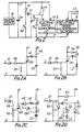
- a previously-proposed circuit includes a voltage source 10 arranged to charge an energy storage capacitor CM (and other capacitors elsewhere in the circuit) to a voltage V1. Also connected across the storage capacitor CM are a series combination of energising switch SW and resistor R1, and a capacitor C1 with triggering coil L1 also connected across switch SW. A secondary of the triggering coil L1 triggers a flash tube FT which is also connected to electronic switch circuit 11 for controlling cut-off of the flash tube FT.
- the switch circuit 11 is responsive to a light-sensing calculation circuit 12 which is connected to a light sensor LS.
- the operation of the Figure 1 circuit is broadly as follows.
- the switch SW When the switch SW is closed (this switch being generally provided in the camera in association with the shutter), the trigger coil L1 generates a pulse signal by virtue of the previously-charged capacitor C1 discharging through the switch SW and coil L1, the pulse signal firing the flash tube FT.
- the light-sensing circuit 12 calculates when sufficient light has been emitted by the photoflash and provides a quenching signal at terminal C which turns off the switch circuit 11 and hence the flash tube FT. This is similar in operation to the circuit illustrated in the Figure of U.S 4288722.
- capacitor C3 (equivalentto capacitor 15 in U.S 4288722) is charged by voltage source 10.
- thyristor switch CR1 is turned on by currentflowthrough capacitors C3, C4and resistor R4 which in turn provides a current path for the flash tube FT which emits light.
- the quenching signal at terminal C turns on the thyristor switch CR2.
- FIG. 1 B will next be referred to in explanation of the generation of the quenching signal at terminal C.
- the circuit acts to integrate the light- responsive signal produced by a photodiode PD acting as photosensor. Initially, capacitor C6 is charged but, during the duration of light emission by the flash tube FT, the capacitor C6 is discharged via resistor R7, flash tube FT and switch CR1. When the photodiode PD has received the required quantity of light, this will have effectively been integrated by the capacitor C8 to a sufficient level to switch on the thyristor CR3 and generate the quenching signal (via capacitor C7) on terminal C.
- the means by which the flash tube of the preferred embodiment of the present invention is turned off differs in principle from that previously described, and provides an accurate and reproducible method of switching.
- This method relies on inductive resonant charging of a capacitor within the switching timing circuit to produce an opposite polarity voltage used to turn off the thyristor, rather than the clamping of an already-charged capacitor as previously described.
- FIG. 2 The circuit of Figure 2 is similarto that of Figure 1 with the exception that there are two connections E, F between the electronic switch circuit 14 and the light-sensing circuit 15, and a further winding from the trigger coil L1 to the switch circuit 14.
- Figures 2A and 2B show two broadly similarforms of switch circuit 14, but in this case there is no automatic light sensing by a circuit such as the calculator 15, and turn-off of the flash tube is achieved a predetermined time after turn-on, i.e. a set quantity of lightwill be emitted, and the camera will need to be adjusted in respect of exposure settings dependent on the distance of the subject from the camera, etc.
- capacitors CM, C1 and C2 are charged when power is applied to the circuit from voltage source 10.
- the switch SW When the switch SW is closed, charge in the capacitor C1 is discharged via the triggering coil L1 which provides a triggering pulse to the flash tube FT and also to the switch circuit at terminal C.
- the pulse at terminal C triggers thyristor CR1 (via diode D1 and resistor R2) and accordingly current flows through the flash tube FT which emits light by discharge of the main capacitor CM.
- charge from capacitor C2 flows through coil L2 and thyristor CR1 and the back e.m.f.
- FIGS 2C and 2D show two further switch circuits which operate in a somewhat similar manner to those of Figures 2A and 2B but include automatic flash quenching by the light sensing circuit 15. Turn-on of thyristor CR1 and consequent light emission from flash tube FT occurs exactly as previously described; however, when capacitor C2 has become charged to a negative potential by inductive resonant charging, it cannot apply that negative potential to the anode of thyristor CR1 because of the blocking action of diode D2.
- Figures 2E and 2F show two forms of light sensing circuit (15 in Figure 2) which utilise bridge arrangements rather than the integrating circuit of the previously-proposed device.
- the illustrated circuits derive power from the charge across capacitor C2 (in Figures 2C and 2D) fed via terminal E to voltage controller VC providing two potentials E1 and E2.
- a capacitor C3 connected across the light sensor LS (phototransistor PT in Figure 2E and photodiode PD in Figure 2F) is charged by the potential E1.
- the potential E2 is supplied to an amplifier circuit which comprises a suitable amplifying element CR3, such as a transistor, thyristor or uni-junction transistor, and is compared to the potential E1. When the circuit is in balance, no signal is provided on terminal F.
- the capacitor C3 discharges current in accordance with that variation.
- the circuit goes out of balance, triggering the amplifier circuit and generating a quench signal at terminal F (which acts as previously described to stop illumination of the flash tube FT).
- FIG. 2G shows one form of voltage controller VC usable in the circuit of Figure 2F.
- a similar controller could be used in the circuit of Figure 2E but with the polarity-sensitive components (e.g. diodes) reversed.
- the two potentials E1 and E2 are derived from two series- connected zener diodes D4, D5 fed via resistors R10, R11 and a blocking diode D3 from the potential on capacitor C2 ( Figure 2D) via the terminal E.
Landscapes
- Stroboscope Apparatuses (AREA)
- Discharge-Lamp Control Circuits And Pulse- Feed Circuits (AREA)
Abstract
Claims (9)
Priority Applications (1)
| Application Number | Priority Date | Filing Date | Title |
|---|---|---|---|
| AT84902354T ATE50391T1 (de) | 1983-06-01 | 1984-06-01 | Elektronische photoblitzlichtsteuerschaltung. |
Applications Claiming Priority (2)
| Application Number | Priority Date | Filing Date | Title |
|---|---|---|---|
| GB8315019 | 1983-06-01 | ||
| GB838315019A GB8315019D0 (en) | 1983-06-01 | 1983-06-01 | Electronic photoflash control circuit |
Publications (2)
| Publication Number | Publication Date |
|---|---|
| EP0146599A1 EP0146599A1 (fr) | 1985-07-03 |
| EP0146599B1 true EP0146599B1 (fr) | 1990-02-07 |
Family
ID=10543635
Family Applications (1)
| Application Number | Title | Priority Date | Filing Date |
|---|---|---|---|
| EP84902354A Expired EP0146599B1 (fr) | 1983-06-01 | 1984-06-01 | Circuit de commande de flash electronique |
Country Status (6)
| Country | Link |
|---|---|
| US (1) | US4798996A (fr) |
| EP (1) | EP0146599B1 (fr) |
| JP (1) | JPS60501483A (fr) |
| DE (1) | DE3481366D1 (fr) |
| GB (2) | GB8315019D0 (fr) |
| WO (1) | WO1984004866A1 (fr) |
Families Citing this family (2)
| Publication number | Priority date | Publication date | Assignee | Title |
|---|---|---|---|---|
| US5189344A (en) * | 1991-05-03 | 1993-02-23 | Public Safety Equipment, Inc. | Solid state strobe tube control circuit with programmable flash pattern |
| DE69433228T2 (de) * | 1993-12-14 | 2004-05-06 | Fuji Photo Film Co., Ltd., Minami-Ashigara | Elektronische Prüfvorrichtung für eine Blitzlichteinheit |
Family Cites Families (5)
| Publication number | Priority date | Publication date | Assignee | Title |
|---|---|---|---|---|
| US3875471A (en) * | 1974-01-18 | 1975-04-01 | Berkey Photo Inc | Photoflash source control circuit |
| US3974419A (en) * | 1975-05-27 | 1976-08-10 | Honeywell Inc. | Electronic flash apparatus with inhibition of contact bounce false triggering |
| US4092565A (en) * | 1976-11-22 | 1978-05-30 | General Electric Company | Pulse circuit for gaseous discharge lamps |
| US4132923A (en) * | 1976-07-01 | 1979-01-02 | Braun Aktiengesellschaft | Circuit for light-integrator-controlled electronic flash unit |
| JPS5536850A (en) * | 1978-09-07 | 1980-03-14 | Canon Inc | Electronic flash device |
-
1983
- 1983-06-01 GB GB838315019A patent/GB8315019D0/en active Pending
-
1984
- 1984-06-01 EP EP84902354A patent/EP0146599B1/fr not_active Expired
- 1984-06-01 US US06/692,883 patent/US4798996A/en not_active Expired - Fee Related
- 1984-06-01 DE DE8484902354T patent/DE3481366D1/de not_active Expired - Lifetime
- 1984-06-01 JP JP59502355A patent/JPS60501483A/ja active Pending
- 1984-06-01 GB GB08501213A patent/GB2161956B/en not_active Expired
- 1984-06-01 WO PCT/GB1984/000191 patent/WO1984004866A1/fr not_active Ceased
Also Published As
| Publication number | Publication date |
|---|---|
| EP0146599A1 (fr) | 1985-07-03 |
| GB2161956B (en) | 1987-05-28 |
| JPS60501483A (ja) | 1985-09-05 |
| US4798996A (en) | 1989-01-17 |
| GB2161956A (en) | 1986-01-22 |
| WO1984004866A1 (fr) | 1984-12-06 |
| DE3481366D1 (de) | 1990-03-15 |
| GB8315019D0 (en) | 1983-07-06 |
| GB8501213D0 (en) | 1985-02-20 |
Similar Documents
| Publication | Publication Date | Title |
|---|---|---|
| US4275335A (en) | Constant light intensity electronic flash device | |
| US4951081A (en) | Flash device | |
| US3809951A (en) | Electronic photoflash | |
| US4228381A (en) | Flash tube apparatus with delayed emission | |
| US6009281A (en) | Flash device | |
| EP0146599B1 (fr) | Circuit de commande de flash electronique | |
| US4351600A (en) | Flash output control failure warning device of an automatic flash output control speed light | |
| US4382211A (en) | Electric flash device | |
| US4354750A (en) | Flash unit having a flash output control device | |
| US4336583A (en) | Controlled inductive storage DC-to-DC converter | |
| US4210849A (en) | Electronic control circuitry for terminating flash output | |
| US3849703A (en) | Electronic flash apparatus | |
| US5668445A (en) | Electronic flash apparatus with constant duration repeated flash | |
| US4561751A (en) | Flash device | |
| US4085353A (en) | Remote sensor trigger circuit | |
| JPH0220088B2 (fr) | ||
| US4132923A (en) | Circuit for light-integrator-controlled electronic flash unit | |
| JPS629890B2 (fr) | ||
| US4274723A (en) | Auto electronic flash unit | |
| US4029992A (en) | Flash apparatus with flash terminating switch controlled by photosensor | |
| US3976913A (en) | Automatic flash device | |
| GB2125978A (en) | Photographic flash device | |
| JPS6227365B2 (fr) | ||
| US4097880A (en) | Photographic stroboscope | |
| US4395658A (en) | Proper light emission indicating device for computer flash device |
Legal Events
| Date | Code | Title | Description |
|---|---|---|---|
| PUAI | Public reference made under article 153(3) epc to a published international application that has entered the european phase |
Free format text: ORIGINAL CODE: 0009012 |
|
| 17P | Request for examination filed |
Effective date: 19850124 |
|
| AK | Designated contracting states |
Designated state(s): AT BE CH DE FR GB LI LU NL SE |
|
| 17Q | First examination report despatched |
Effective date: 19870429 |
|
| GRAA | (expected) grant |
Free format text: ORIGINAL CODE: 0009210 |
|
| AK | Designated contracting states |
Kind code of ref document: B1 Designated state(s): AT BE CH DE FR GB LI LU NL SE |
|
| REF | Corresponds to: |
Ref document number: 50391 Country of ref document: AT Date of ref document: 19900215 Kind code of ref document: T |
|
| ET | Fr: translation filed | ||
| REF | Corresponds to: |
Ref document number: 3481366 Country of ref document: DE Date of ref document: 19900315 |
|
| PLBE | No opposition filed within time limit |
Free format text: ORIGINAL CODE: 0009261 |
|
| STAA | Information on the status of an ep patent application or granted ep patent |
Free format text: STATUS: NO OPPOSITION FILED WITHIN TIME LIMIT |
|
| 26N | No opposition filed | ||
| EPTA | Lu: last paid annual fee | ||
| EAL | Se: european patent in force in sweden |
Ref document number: 84902354.4 |
|
| PGFP | Annual fee paid to national office [announced via postgrant information from national office to epo] |
Ref country code: GB Payment date: 19950522 Year of fee payment: 12 |
|
| PGFP | Annual fee paid to national office [announced via postgrant information from national office to epo] |
Ref country code: DE Payment date: 19950607 Year of fee payment: 12 |
|
| PGFP | Annual fee paid to national office [announced via postgrant information from national office to epo] |
Ref country code: FR Payment date: 19950609 Year of fee payment: 12 |
|
| PGFP | Annual fee paid to national office [announced via postgrant information from national office to epo] |
Ref country code: AT Payment date: 19950613 Year of fee payment: 12 |
|
| PGFP | Annual fee paid to national office [announced via postgrant information from national office to epo] |
Ref country code: CH Payment date: 19950614 Year of fee payment: 12 |
|
| PGFP | Annual fee paid to national office [announced via postgrant information from national office to epo] |
Ref country code: SE Payment date: 19950615 Year of fee payment: 12 |
|
| PGFP | Annual fee paid to national office [announced via postgrant information from national office to epo] |
Ref country code: NL Payment date: 19950628 Year of fee payment: 12 |
|
| PGFP | Annual fee paid to national office [announced via postgrant information from national office to epo] |
Ref country code: LU Payment date: 19950701 Year of fee payment: 12 |
|
| PGFP | Annual fee paid to national office [announced via postgrant information from national office to epo] |
Ref country code: BE Payment date: 19950712 Year of fee payment: 12 |
|
| PG25 | Lapsed in a contracting state [announced via postgrant information from national office to epo] |
Ref country code: LU Free format text: LAPSE BECAUSE OF NON-PAYMENT OF DUE FEES Effective date: 19960601 Ref country code: GB Effective date: 19960601 Ref country code: AT Effective date: 19960601 |
|
| PG25 | Lapsed in a contracting state [announced via postgrant information from national office to epo] |
Ref country code: SE Effective date: 19960602 |
|
| PG25 | Lapsed in a contracting state [announced via postgrant information from national office to epo] |
Ref country code: LI Effective date: 19960630 Ref country code: CH Effective date: 19960630 Ref country code: BE Effective date: 19960630 |
|
| BERE | Be: lapsed |
Owner name: LAM SHEIR CHUN Effective date: 19960630 |
|
| PG25 | Lapsed in a contracting state [announced via postgrant information from national office to epo] |
Ref country code: NL Effective date: 19970101 |
|
| GBPC | Gb: european patent ceased through non-payment of renewal fee |
Effective date: 19960601 |
|
| REG | Reference to a national code |
Ref country code: CH Ref legal event code: PL |
|
| PG25 | Lapsed in a contracting state [announced via postgrant information from national office to epo] |
Ref country code: FR Effective date: 19970228 |
|
| PG25 | Lapsed in a contracting state [announced via postgrant information from national office to epo] |
Ref country code: DE Effective date: 19970301 |
|
| EUG | Se: european patent has lapsed |
Ref document number: 84902354.4 |
|
| NLV4 | Nl: lapsed or anulled due to non-payment of the annual fee |
Effective date: 19970101 |
|
| REG | Reference to a national code |
Ref country code: FR Ref legal event code: ST |