EP0146834A2 - Positive photoresist developer - Google Patents
Positive photoresist developer Download PDFInfo
- Publication number
- EP0146834A2 EP0146834A2 EP84114722A EP84114722A EP0146834A2 EP 0146834 A2 EP0146834 A2 EP 0146834A2 EP 84114722 A EP84114722 A EP 84114722A EP 84114722 A EP84114722 A EP 84114722A EP 0146834 A2 EP0146834 A2 EP 0146834A2
- Authority
- EP
- European Patent Office
- Prior art keywords
- developer
- development
- ppm
- positive photoresist
- surfactants
- Prior art date
- Legal status (The legal status is an assumption and is not a legal conclusion. Google has not performed a legal analysis and makes no representation as to the accuracy of the status listed.)
- Withdrawn
Links
Classifications
-
- G—PHYSICS
- G03—PHOTOGRAPHY; CINEMATOGRAPHY; ANALOGOUS TECHNIQUES USING WAVES OTHER THAN OPTICAL WAVES; ELECTROGRAPHY; HOLOGRAPHY
- G03F—PHOTOMECHANICAL PRODUCTION OF TEXTURED OR PATTERNED SURFACES, e.g. FOR PRINTING, FOR PROCESSING OF SEMICONDUCTOR DEVICES; MATERIALS THEREFOR; ORIGINALS THEREFOR; APPARATUS SPECIALLY ADAPTED THEREFOR
- G03F7/00—Photomechanical, e.g. photolithographic, production of textured or patterned surfaces, e.g. printing surfaces; Materials therefor, e.g. comprising photoresists; Apparatus specially adapted therefor
- G03F7/26—Processing photosensitive materials; Apparatus therefor
- G03F7/30—Imagewise removal using liquid means
- G03F7/32—Liquid compositions therefor, e.g. developers
- G03F7/322—Aqueous alkaline compositions
Definitions
- the invention relates to a developer for positive photoresists with improved properties with regard to the resolution and edge steepness which can be achieved in the developed resist image, and with regard to its development activity, capacity and stability.
- Photoresist materials of both positive and negative types are used in a variety of ways in the photolithographic transfer of image structures.
- positive photoresist materials are particularly important because they guarantee the best possible resolution today when transferring the finest image structures to conductor and semiconductor substrates.
- the latter is coated with the resist material in the form of a lacquer and then an image pattern is transferred to the photoresist layer by exposure, for example through a mask.
- the exposed photoresist areas are detached, which then creates a positive relief image on the substrate.
- a further structuring or modification, for example by etching, can now be carried out on the exposed substrate regions Metal coating or doping.
- the positive photoresist materials used are usually photosensitive compositions based on phenol-formaldehyde condensates of the novolak type as resin components and compounds of the o-diazoquinone type as photosensitive components.
- the solubility of the exposed photoresist areas in an aqueous-alkaline environment is drastically increased by the action of light, usually in the UV range.
- Such positive photoresist materials can thus be developed in aqueous alkaline developer systems.
- the influences of the developer during development are decisive for the quality of the positive photo relief relief structures to be obtained with regard to resolution, edge structure, remaining layer thickness and surface quality.
- Prior art developers for positive photoresist are usually aqueous solutions of compounds which cause an alkaline pH.
- alkalis such as alkali hydroxides, or alkali metal salts such as A lkalisilikate or phosphates.
- the developers can be buffered to stabilize the pH of the solution and contain a wide variety of surfactants to improve the wettability
- the known developers have the disadvantage that they also attack non-exposed image areas of the resist layer to a not inconsiderable extent and cause significant layer removal. This is particularly evident in the border areas between the exposed and unexposed parts of the image, where the 90 ° edges of the remaining resist relief structures, which are ideally aimed for, are considerably beveled and rounded off by the layer removal by the developer. This leads to only a moderate contrast, a significant reduction in the possible and predetermined resolution by the optical parameters and an inaccurate image reproduction for the subsequent processes such as etching, coating or doping of the substrate.
- the invention was therefore based on the object of finding a developer for positive photoresists which has significantly improved properties with regard to the resolution and edge steepness to be achieved in the resist image and with regard to stability, development activity and capacity.
- a developer for positive photoresists based on a buffered, nonionic surfactant-containing aqueous alkaline solution which contains 1-100 ppm of these surfactants in the solution, has excellent development properties and a long stability.
- the invention thus relates to developers for positive photoresists based on a buffered, nonionic surfactant-containing aqueous alkaline solution which contains 1-100 ppm, preferably 10-60 ppm, in particular 30-50 ppm of the surfactants in the solution.
- the invention relates to such a developer that contains surfactants of the ethoxylated alkylphenol type.
- the invention further relates to a method for developing positive photoresist relief structures by treating an exposed positive photoresist coating with a developer solution, such a developer being used.
- DE-OS 32 23 386 / USP 4,374,920 describes aqueous alkaline developers which also contain nonionic surfactants, but which are primarily tailored to the production of printing plates.
- the stated concentrations of 0.1-10% by weight of surfactant (corresponding to 1000 to 100000 ppm) have the task here of protecting the printing plate material exposed during development from etching by the developer.
- These developers are not suitable for the production of highly and highly integrated electronic circuits and components.
- USP 3,586,504 describes developers based on aqueous sodium hydroxide solution for producing metal masks in microelectronics which contain nonionic surfactants of the special type of alkylphenoxypoly (hydroxyalkylene oxides) in a proportion of at least 0.05% by weight (corresponding to 500 ppm). These developers also do not meet today's requirements with regard to the resolution and edge steepness that can be achieved in the resist image.
- non-ionic surfactants are suitable as surfactant additives.
- Nonionic surfactants of the ethoxylated alkylphenol type are advantageous. Ethoxylation products of alkylphenols having 6 to 14 carbon atoms in the alkyl chain and degrees of ethoxylation of 2 to 20 are commercially available ethoxylated nonylphenol with an average degree of ethoxylation of about 9.
- the excellent development properties of the developer according to the invention are achieved in that it contains 1 to 100 ppm, preferably 10 to 60 ppm, in particular 30 to 50 ppm of such surfactants.
- the developer according to the invention leaves the unexposed image areas of the positive photoresist layer practically completely unaffected and is only above a minimum exposure energy, which may vary with different photoresists, but mostly around 1 0 m J / cm 2 , based on 1 ⁇ m layer thickness , quickly and completely peels the exposed parts of the image down to the substrate.
- a layer removal by the developer in the unexposed areas is minimal, if recognizable at all, and is less than 5%.
- the surface of the resist layer remaining after development is smooth and even and in particular does not show the depressions known as "pinholes", which are otherwise very common and particularly feared.
- the developer according to the invention removes the exposed photoresist image areas at high speed and completely, so that relief structures with a previously unachieved contrast and with a resolution that is only limited by the optical parameters are obtained.
- the remaining relief structures show almost ideal 90 ° edges without roundings and bevels.
- Another advantage of the developer according to the invention is the wide temporal scope for development that this enables. Despite the high development activity, which is shown in a particularly rapid removal of the exposed resist material, the unexposed image areas are not attacked if the substrate coated with the resist remains in the developer solution for a long time; there are also no overdevelopments. This property makes the development process much less problematic; Complex development endpoint controls in the process flow can be largely or completely dispensed with.
- the developer according to the invention exhibits excellent stability both in storage and in use.
- the composition remains remarkably constant; Turbidity and flocculation, which are extremely disruptive in the manufacture of microelectronic circuits and components, are not observed. Due to this unusual stability, the developer has a higher development capacity, so that same volumes of the developer solution at a substantially longer stability and reproducibility of E ntwicklungsures can be better exploited.
- the developer according to the invention is produced in a manner known per se.
- the individual constituents are dissolved in their quantitative proportions in water, which should advantageously be fully desalinated and, if possible, degassed, with heating.
- Corresponding purity criteria are common among experts under the name "electronic grade”.
- the remaining components of the developer are known from the prior art.
- the developers generally contain alkali compounds which can split off hydroxyl ions in aqueous solution. These include e.g. Alkali silicates, alkali metasilicate, alkali phosphates and alkali hydroxide. These substances which bring about the alkaline pH are generally present in the developer in an amount of approximately 1-6% by weight, preferably approximately 2-5% by weight, based on the total amount of the developer solution.
- sodium or potassium metasilicate preferably sodium metasilicate pentahydrate
- all alkali salts of weak inorganic acids or mixtures thereof which are common for such purposes can be used as buffer substances.
- Potassium and sodium phosphate buffers for example based on primary, secondary and / or tertiary sodium and potassium phosphates, are particularly suitable and therefore preferred.
- the most favorable development properties are achieved if the pH of the developer is in the range between 12 and 14, preferably between 12.5 and 13.5.
- the pH can be adjusted by the controlled addition of alkali metal hydroxide.
- the developer according to the invention can in principle be used to develop all positive photoresist materials which are essentially based on mixtures of resin components of the novolak type and light-sensitive components of the o-diazoquinone type.
- these are mixtures of condensation products of formaldehyde with phenols or compounds containing phenolic hydroxyl groups and naphthoquinonediazide sulfonyl derivatives.
- Such photoresist compositions are widely known and described for example in the patents DE-PS 938 233 / USP 3,106,465, DE-PS 11 95 166 / USP 3,201,239 and the German patent applications P 32 20 816 and P 33 44 202.
- a commercially available positive photoresist lacquer based on a 5-oxo-6-diazo-5,6-dihydronaphthalenesulfonic acid ester and a cresol-formaldehyde novolak resin is applied by spin-coating onto silicon wafer thermally oxidized on the surface.
- the layer thickness after a 30-minute predrying at 90 ° is 1.2 ⁇ m.
- the wafers are then exposed at different times in a contact exposure process through a mask with a line pattern with a 200 W mercury lamp and an intensity of 6.5 mW / cm 2 at 365 nm.
- the wafers are then developed in the developer according to a) at 22 ° C. for 60 seconds. After development, the relief structures obtained are examined and the remaining layer thickness is measured.
- a scanning electron microscope evaluation of the structures in the photoresist shows that patterns with a structure width of 1 ⁇ m and below are neatly developed and high-resolution from an exposure time of 2 seconds, while a layer removal of less than 5 in exposure times under 2 seconds or in the unexposed areas % can be determined.
- the relief images show smooth, flat surfaces without depressions with sharp, steep edges without roundings or bevels. Deposits of contaminants cannot be seen on the resist image or on the exposed substrate.
- Example la but with 0.1% by weight ( ⁇ 1000 ppm) of the surfactant.
- the relief images show uneven surfaces and strongly rounded or beveled transitions in the border areas between the resist and the exposed substrate.
Landscapes
- Physics & Mathematics (AREA)
- General Physics & Mathematics (AREA)
- Photosensitive Polymer And Photoresist Processing (AREA)
- Exposure Of Semiconductors, Excluding Electron Or Ion Beam Exposure (AREA)
- Non-Silver Salt Photosensitive Materials And Non-Silver Salt Photography (AREA)
Abstract
Ein Entwickler für Positiv-Fotoresists auf Basis einer gepufferten, nichtionogene Tenside enthaltenden wässerig-alkalischen Lösung, der in der Lösung 1 - 100 ppm der Tenside, vorzugsweise vom Typ der ethoxylierten Alkylphenole, enthält, ziegt hervorragende Eigenschaften hinsichtlich der im entwickelten Resistbild zu erzielenden Auflösung und Kantensteilheit sowie hinsichtlich seiner Entwicklungsaktivität, -kapazität und Stabilität.A developer for positive photoresists based on a buffered, nonionic surfactant-containing aqueous alkaline solution, which contains 1-100 ppm of the surfactants, preferably of the ethoxylated alkylphenol type, has excellent properties with regard to the resolution to be achieved in the resist image developed and edge steepness, as well as its development activity, capacity and stability.
Description
Die Erfindung betrifft einen Entwickler für Positiv- Fotoresists mit verbesserten Eigenschaften hinsichtlich der im entwickelten Resistbild erzielbaren Auflösung und Kantensteilheit sowie hinsichtlich seiner Entwicklungsaktivität, -kapazität und Stabilität.The invention relates to a developer for positive photoresists with improved properties with regard to the resolution and edge steepness which can be achieved in the developed resist image, and with regard to its development activity, capacity and stability.
Fotoresistmaterialien sowohl vom Positiv- als auch von Negativtyp werden bei der fotolithographischen Übertragung von Bildstrukturen in vielfältiger Weise eingesetzt.Photoresist materials of both positive and negative types are used in a variety of ways in the photolithographic transfer of image structures.
In der Halbleitertechnologie und Mikroelektronik genießen Positivfotoresistmaterialien besondere Bedeutung, da sie bei der Übertragung von feinsten Bildstrukturen auf Leiter- und Halbleitersubstrate die heute immer noch bestmögliche Auflösung gewährleisten.In semiconductor technology and microelectronics, positive photoresist materials are particularly important because they guarantee the best possible resolution today when transferring the finest image structures to conductor and semiconductor substrates.
Zur Erzeugung von Positivresistbildern auf einem Substrat wird dieses mit dem Resistmaterial in Form eines Lackes beschichtet und dann ein Bildmuster durch Belichtung, beispielsweise durch eine Maske hindurch, auf die Fotolackschicht übertragen. In einem anschließenden Entwicklungsprozeß werden die belichteten Fotolackbereiche abgelöst, wodurch dann auf dem Substrat ein positives Reliefbild entsteht. An den freigelegten Substratbereichen kann nun eine weitere Strukturierung oder Modifizierung, beispielsweise durch eine Ätzung, durch Metallbeschichtung oder Dotierung erfolgen.To produce positive resist images on a substrate, the latter is coated with the resist material in the form of a lacquer and then an image pattern is transferred to the photoresist layer by exposure, for example through a mask. In a subsequent development process, the exposed photoresist areas are detached, which then creates a positive relief image on the substrate. A further structuring or modification, for example by etching, can now be carried out on the exposed substrate regions Metal coating or doping.
Die eingesetzten Positivfotoresistmaterialien sind üblicherweise lichtempfindliche Zusammensetzungen auf Basis von Phenol-Formaldehyd-Kondensaten vom Novolaktyp als Harzkomponenten und Verbindungen vom Typ der o-Diazochinone als lichtempfindliche Komponenten. Durch die Einwirkung von Licht, üblicherweise des UV-Bereichs, wird die Löslichkeit der belichteten Fotolackbereiche in einem wässerig-alkalischem Milieu drastisch erhöht. Solche Positivfotoresistmaterialien sind somit in wässerig-alkalischen Entwicklersystemen entwickelbar.The positive photoresist materials used are usually photosensitive compositions based on phenol-formaldehyde condensates of the novolak type as resin components and compounds of the o-diazoquinone type as photosensitive components. The solubility of the exposed photoresist areas in an aqueous-alkaline environment is drastically increased by the action of light, usually in the UV range. Such positive photoresist materials can thus be developed in aqueous alkaline developer systems.
Die fortschreitende Miniaturisierung in der Halbleitertechnologie, insbesondere die VLSI-Technik (very large scale integration) zur Herstellung hoch- und höchstintegrierter elektronischer Bauelemente und Schaltungen erfordert ein Höchstmaß an Reproduktionsgenauigkeit bei diesen fotolithographischen Prozessen. Hierbei kommt dem Prozeßschritt der Entwicklung besondere Bedeutung zu.The advancing miniaturization in semiconductor technology, in particular VLSI technology (very large scale integration) for the production of highly and highly integrated electronic components and circuits requires a high degree of reproducibility in these photolithographic processes. The process step of development is of particular importance here.
Maßgeblich für die Qualität der zu erhaltenden Positivfotoresistreliefstrukturen in Bezug auf Auflösung, Kantenstruktur, verbleibender Schichtdicke und Oberflächenbeschaffenheit sind neben der Präzision der Belichtungsapparatur und den Eigenschaften des Fotolacks insbesondere die Einflüsse des Entwicklers während der Entwicklung.In addition to the precision of the exposure apparatus and the properties of the photoresist, the influences of the developer during development are decisive for the quality of the positive photo relief relief structures to be obtained with regard to resolution, edge structure, remaining layer thickness and surface quality.
Entwickler für Positivfotoresist nach dem Stand der Technik sind üblicherweise wässerige Lösungen von einen alkalischen pH-Wert bewirkenden Verbindungen.Prior art developers for positive photoresist are usually aqueous solutions of compounds which cause an alkaline pH.
Meist enthalten sie Alkalien, etwa Alkalihydroxide, oder Alkalisalze wie beispielsweise Alkalisilikate oder -phosphate. Die Entwickler können zur Stabilisierung des pH-Wertes der Lösung gepuffert sein und zur Verbesserung der Benetzungsfähigkeit die verschiedenartigsten Tenside enthaltenThey usually contain alkalis, such as alkali hydroxides, or alkali metal salts such as A lkalisilikate or phosphates. The developers can be buffered to stabilize the pH of the solution and contain a wide variety of surfactants to improve the wettability
Die bekannten Entwickler haben jedoch den Nachteil, daß sie in nicht unbeträchtlichem Maße auch nichtbelichtete Bildbereiche der Resistschicht angreifen und einen deutlichen Schichtabtrag bewirken. Dies wird insbesondere auch in den Grenzbereichen zwischen den belichteten und nichtbelichteten Bildteilen deutlich, wo durch den Schichtabtrag des Entwicklers die im Idealfall anzustrebenden 90°-Kanten der verbleibenden Resistreliefstrukturen erheblich eingeschrägt und abgerundet werden. Dies führt zu einem nur mäßigen Kontrast, einer deutlichen Verringerung der durch die optischen Parameter vorgegebenen und möglichen Auflösung und einer ungenauen Bildwiedergabe für die nachfolgenden Prozesse wie Ätzen, Beschichten oder Dotieren des Substrats.However, the known developers have the disadvantage that they also attack non-exposed image areas of the resist layer to a not inconsiderable extent and cause significant layer removal. This is particularly evident in the border areas between the exposed and unexposed parts of the image, where the 90 ° edges of the remaining resist relief structures, which are ideally aimed for, are considerably beveled and rounded off by the layer removal by the developer. This leads to only a moderate contrast, a significant reduction in the possible and predetermined resolution by the optical parameters and an inaccurate image reproduction for the subsequent processes such as etching, coating or doping of the substrate.
Weiterhin haben bekannte Entwickler nur eine begrenzte Stabilität und Entwicklungskapazität. Sie zeigen bei Lagerung und Benutzung Veränderungen in der Zusammensetzung, so daß die Reproduzierbarkeit der Entwicklungsergebnisse nicht über längere Dauer gewährleistet ist. Es ist deshalb üblich, die Entwicklungsprozesse mit aufwendigen apparativen Maßnahmen am zu entwickelnden Substrat fortlaufend zu überwachen und den Entwicklungsendpunkt festzustellen. Darüber hinaus werden Ausflockungen und Ablagerungen von Verunreinigungen und Abbauprodukten von Entwickler und Resistmaterial in der Entwicklerlösung und - besonders störend - auf dem Substrat beobachtet.Furthermore, known developers have only limited stability and development capacity. They show changes in the composition during storage and use, so that the reproducibility of the development results is not guaranteed over a longer period. It is therefore common to continuously monitor the development processes with complex equipment measures on the substrate to be developed and to determine the end point of development. In addition, flocculation and deposits of contaminants and degradation products from developer and resist material in the Developer solution and - particularly disturbing - observed on the substrate.
Es besteht daher Bedarf an verbesserten Positivfotoresistentwicklern für die Mikroelektronik, insbesondere die VLSI-Technik.There is therefore a need for improved positive photoresist developers for microelectronics, especially VLSI technology.
Der Erfindung lag somit die Aufgabe zugrunde, einen Entwickler für Positivfotoresists zu finden, der hinsichtlich der im Resistbild zu erzielenden Auflösung und Kantensteilheit sowie hinsichtlich Stabilität, Entwicklungsaktivität und -kapazität deutlich verbesserte Eigenschaften aufweist.The invention was therefore based on the object of finding a developer for positive photoresists which has significantly improved properties with regard to the resolution and edge steepness to be achieved in the resist image and with regard to stability, development activity and capacity.
Überraschend wurde nun gefunden, daß ein Entwickler für Positivfotoresists auf Basis einer gepufferten, nichtionogene Tenside enthaltenden wässerig-alkalischen Lösung, der in der Lösung 1 - 100 ppm dieser Tenside enthält, ausgezeichnete Entwicklungseigenschaften sowie eine lange Stabilität besitzt.Surprisingly, it has now been found that a developer for positive photoresists based on a buffered, nonionic surfactant-containing aqueous alkaline solution, which contains 1-100 ppm of these surfactants in the solution, has excellent development properties and a long stability.
Gegenstand der Erfindung sind somit Entwickler für Positivfotoresists auf Basis einer gepufferten, nichtionogene Tenside enthaltenden wässerig-alkalischen Lösung, der in der Lösung 1 - 100 ppm, vorzugsweise 10 - 60 ppm, insbesondere 30 - 50 ppm der Tenside enthält. Insbesondere ist Gegenstand der Erfindung ein solcher Entwickler, der Tenside vom Typ der ethoxylierten Alkylphenole enthält.The invention thus relates to developers for positive photoresists based on a buffered, nonionic surfactant-containing aqueous alkaline solution which contains 1-100 ppm, preferably 10-60 ppm, in particular 30-50 ppm of the surfactants in the solution. In particular, the invention relates to such a developer that contains surfactants of the ethoxylated alkylphenol type.
Weiterhin ist Gegenstand der Erfindung ein Verfahren zur Entwicklung von Positivfotoresistreliefstrukturen durch Behandlung einer belichteten Positivfotoresistbeschichtung mit einer Entwicklerlösung, wobei ein solcher Entwickler eingesetzt wird.The invention further relates to a method for developing positive photoresist relief structures by treating an exposed positive photoresist coating with a developer solution, such a developer being used.
Zwar sind Entwickler für Positiv-Fotolack-Beschichtungen mit ähnlichen oder z.T. gleichen Inhaltsstoffen bekannt; sie weisen jedoch wesentlich höhere Tensidkonzentrationen auf und entsprechen in ihren Entwicklungseigenschaften nicht den heutigen Anforderungen an die VLSI-Technik.Although developers for positive photoresist coatings with similar or partially same ingredients known; however, they have much higher surfactant concentrations and their development properties do not meet today's requirements for VLSI technology.
So werden beispielsweise in der DE-OS 32 23 386 /USP 4,374,920 wässerig-alkalische Entwickler, die auch nichtionogene Tenside enthalten, beschrieben, die jedoch vornehmlich auf die Herstellung von Druckplatten zugeschnitten sind. Die angegebenen Konzentrationen von 0.1 - 10 Gew.% an Tensid (entsprechend 1000 bis 100000 ppm) haben hier die Aufgabe, das bei der Entwicklung freigelegte Druckplattenmaterial von einer Anätzung durch den Entwickler zu schützen. Diese Entwickler sind für die Herstellung hoch- und höchstintegrierter elektronischer Schaltungen und Bauelemente nicht geeignet.For example, DE-OS 32 23 386 / USP 4,374,920 describes aqueous alkaline developers which also contain nonionic surfactants, but which are primarily tailored to the production of printing plates. The stated concentrations of 0.1-10% by weight of surfactant (corresponding to 1000 to 100000 ppm) have the task here of protecting the printing plate material exposed during development from etching by the developer. These developers are not suitable for the production of highly and highly integrated electronic circuits and components.
In USP 3,586,504 werden Entwickler auf Basis wässeriger Natronlauge zur Herstellung von Metallmasken in der Mikroelektronik beschrieben, die nichtionogene Tenside vom speziellen Typ der Alkylphenoxypoly(hydroxyalkylen- oxide) in einem Anteil von mindestens 0,05 Gew.% (entsprechend 500 ppm) enthalten. Auch diese Entwickler erfüllen nicht die heutigen Anforderungen im Hinblick auf die im Resistbild zu erzielende Auflösung und Kantensteilheit.USP 3,586,504 describes developers based on aqueous sodium hydroxide solution for producing metal masks in microelectronics which contain nonionic surfactants of the special type of alkylphenoxypoly (hydroxyalkylene oxides) in a proportion of at least 0.05% by weight (corresponding to 500 ppm). These developers also do not meet today's requirements with regard to the resolution and edge steepness that can be achieved in the resist image.
Als Tensidzusatz sind im Prinzip alle nichtionogenen Tenside, sofern sie alkalikompatibel sind, geeignet. Vorteilhaft sind nichtionogene Tenside vom Typ der ethoxylierten Alkylphenole. Kommerziell erhältlich sind Ethoxylierungsprodukte von Alkylphenolen mit 6 - 14 Kohlenstoffatomen in der Alkylkette und Ethoxylierungsgraden von 2 - 20. Besonders bevorzugt ist ein ethoxyliertes Nonylphenol mit einem mittleren Ethoxylierungsgrad von etwa 9. Die hervorragenden Entwicklungseigenschaften des erfindungsgemäßen Entwicklers werden dadurch erreicht, daß in ihm 1 - 100 ppm, vorzugsweise 10 - 60 ppm, insbesondere 30 - 50 ppm an solchen Tensiden enthalten sind.In principle, all non-ionic surfactants, provided they are alkali-compatible, are suitable as surfactant additives. Nonionic surfactants of the ethoxylated alkylphenol type are advantageous. Ethoxylation products of alkylphenols having 6 to 14 carbon atoms in the alkyl chain and degrees of ethoxylation of 2 to 20 are commercially available ethoxylated nonylphenol with an average degree of ethoxylation of about 9. The excellent development properties of the developer according to the invention are achieved in that it contains 1 to 100 ppm, preferably 10 to 60 ppm, in particular 30 to 50 ppm of such surfactants.
Die Vorteile des erfindungsgemäßen Entwicklers gegenüber solchen nach dem Stand der Technik mit ähnlichen oder gleichen Inhaltstoffen zeigen sich in der Eigenschaft, Positivfotoresistreliefstrukturen mit einer bisher nicht erreichbaren Auflösung und Kantensteilheit zu entwickeln.The advantages of the developer according to the invention compared to those according to the prior art with similar or the same constituents are evident in the property of developing positive photo relief relief structures with a resolution and edge steepness that has not been achievable until now.
Es zeigt sich, daß der erfindungsgemäße Entwickler die unbelichteten Bildbereiche der Positivfotoresistschicht praktisch völlig unangegriffen läßt und erst ab einer Mindestbelichtungsenergie, die bei unterschiedlichen Fotolacken zwar variieren kann, meist aber um etwa 10 mJ/cm2, bezogen auf 1 µm Schichtdicke, liegt, die belichteten Bildteile rasch und vollständig bis zum Substrat ablöst.It can be seen that the developer according to the invention leaves the unexposed image areas of the positive photoresist layer practically completely unaffected and is only above a minimum exposure energy, which may vary with different photoresists, but mostly around 1 0 m J / cm 2 , based on 1 μm layer thickness , quickly and completely peels the exposed parts of the image down to the substrate.
Ein Schichtabtrag durch den Entwickler in den unbelichteten Bereichen ist, sofern überhaupt erkennbar, minimal und beträgt weniger als 5%. Die Oberfläche der nach der Entwicklung verbleibenden Resistschicht ist glatt und eben und zeigt insbesondere nicht die sonst sehr häufig auftretenden und besonders gefürchteten, als "pinholes" bezeichneten Vertiefungen. Demgegenüber entfernt der erfindungsgemäße Entwickler die belichteten Fotoresistbildbereiche mit hoher Geschwindigkeit und restlos, so daß Reliefstrukturen mit bisher nicht erreichtem Kontrast und mit praktisch einer nur noch durch die optischen Parameter limitierten Auflösung erhalten werden. Die verbleibenden Reliefstrukturen zeigen nahezu ideale 90°-Kanten ohne Abrundungen und Einschrägungen.A layer removal by the developer in the unexposed areas is minimal, if recognizable at all, and is less than 5%. The surface of the resist layer remaining after development is smooth and even and in particular does not show the depressions known as "pinholes", which are otherwise very common and particularly feared. In contrast, the developer according to the invention removes the exposed photoresist image areas at high speed and completely, so that relief structures with a previously unachieved contrast and with a resolution that is only limited by the optical parameters are obtained. The remaining relief structures show almost ideal 90 ° edges without roundings and bevels.
Ein weiterer Vorteil des erfindungsgemäßen Entwicklers ist der weite zeitliche Entwicklungsspielraum, den dieser ermöglicht. Trotz der hohen Entwicklungsaktivität, die sich in einer besonders raschen Entfernung des belichteten Resistmaterials zeigt, werden bei einem längeren Verbleib des mit dem Resist beschichteten Substrates in der Entwicklerlösung die unbelichteten Bildbereiche nicht angegriffen; auch kommt es nicht zu Überentwicklungen. Durch diese Eigenschaft wird der Entwicklungsprozeß wesentlich unproblematischer; auf aufwendige Entwicklungsendpunktkontrollen im Prozeßablauf kann weitgehend oder vollständig verzichtet werden.Another advantage of the developer according to the invention is the wide temporal scope for development that this enables. Despite the high development activity, which is shown in a particularly rapid removal of the exposed resist material, the unexposed image areas are not attacked if the substrate coated with the resist remains in the developer solution for a long time; there are also no overdevelopments. This property makes the development process much less problematic; Complex development endpoint controls in the process flow can be largely or completely dispensed with.
Es hat sich gezeigt, daß höhere als die angegebenen Tensidkonzentrationen sich ungünstig auswirken; vermutlich treten Aktivitätsverluste durch Passivierung auf. Es werden dann für eine vollständige Entwicklung längere Zeiten erforderlich, die wiederum einen verstärkten Schichtabtrag und Verluste an Kontrast und Auflösung bedingen. Weiterhin werden bei höheren Tensidkonzentrationen als sehr störend empfundene Ablagerungen von Tensid und von Anteilen beziehungsweise Abbauprodukten des Resistmaterials auf den freigelegten Substratbereichen festgestellt.It has been shown that higher than the specified surfactant concentrations have an unfavorable effect; there is likely to be a loss of activity due to passivation. Longer times are then required for complete development, which in turn means increased layer removal and loss of contrast and resolution. Furthermore, at higher surfactant concentrations, deposits of surfactant and portions or degradation products of the resist material, which are perceived as very disturbing, are found on the exposed substrate areas.
Über diese vorteilhaften Entwicklungseigenschaften hinaus zeigt der erfindungsgemäße Entwickler eine hervorragende Stabilität sowohl bei der Lagerung als auch bei Gebrauch. Bei sachgemäßer Herstellung, Lagerung und Verwendung bleibt die Zusammensetzung bemerkenswert konstant; Trübungen und Ausflockungen, die bei der Herstellung von mikroelektronischen Schaltungen und Bauteilen äußerst störend sind, werden nicht beobachtet. Durch diese ungewöhnliche Stabilität verfügt der Entwickler über eine höhere Entwicklungskapazität, so daß gleiche Volumeneinheiten der Entwicklerlösung bei einer wesentlich längeren Konstanz und Reproduzierbarkeit des Entwicklungsergebnisses besser ausgenutzt werden können.In addition to these advantageous development properties, the developer according to the invention exhibits excellent stability both in storage and in use. When properly manufactured, stored and used, the composition remains remarkably constant; Turbidity and flocculation, which are extremely disruptive in the manufacture of microelectronic circuits and components, are not observed. Due to this unusual stability, the developer has a higher development capacity, so that same volumes of the developer solution at a substantially longer stability and reproducibility of E ntwicklungsergebnisses can be better exploited.
Die Herstellung des erfindungsgemäßen Entwicklers erfolgt in an sich bekannter Weise. Hierzu werden die Einzelbestandteile in ihren mengenmäßigen Anteilen in Wasser, das vorteilhafterweise voll entsalzt und möglichst entgast sein sollte, gegebenenfalls unter Erwärmen gelöst. Insgesamt empfiehlt es sich, bei der Auswahl der Ausgangsstoffe auf höchste Reinheit und bei der Herstellung auf peinlichsten Ausschluß von Verunreinigungs- und Störungsmöglichkeiten zu achten. Entsprechende Reinheitskriterien sind in der Fachwelt unter der Bezeichnung "electronic grade" geläufig. Die übrigen Bestandteile des Entwicklers sind aus dem Stand der Technik bekannt. Die Entwickler enthalten im allgemeinen Alkaliverbindungen, die in wässeriger Lösung Hydroxylionen abzuspalten vermögen. Hierzu gehören z.B. Alkalisilikate, Alkalimetasilikat, Alkaliphosphate und Alkalihydroxid. Diese den alkalischen pH-Wert bewirkenden Substanzen sind im Entwickler in der Regel zu etwa 1 - 6 Gew.% enthalten, vorzugsweise etwa 2 - 5 Gew.%, bezogen auf die Gesamtmenge der Entwicklerlösung.The developer according to the invention is produced in a manner known per se. For this purpose, the individual constituents are dissolved in their quantitative proportions in water, which should advantageously be fully desalinated and, if possible, degassed, with heating. Overall, it is advisable to pay attention to the highest purity when selecting the starting materials and to embarrassingly exclude the possibility of contamination and disruption during manufacture. Corresponding purity criteria are common among experts under the name "electronic grade". The remaining components of the developer are known from the prior art. The developers generally contain alkali compounds which can split off hydroxyl ions in aqueous solution. These include e.g. Alkali silicates, alkali metasilicate, alkali phosphates and alkali hydroxide. These substances which bring about the alkaline pH are generally present in the developer in an amount of approximately 1-6% by weight, preferably approximately 2-5% by weight, based on the total amount of the developer solution.
Bevorzugt ist ein Zusatz an Natrium- oder Kaliummetasilikat, vorzugsweise Natriummetasilikatpentahydrat. Als Puffersubstanzen kommen im Prinzip alle für solche Zwecke gängigen Alkalisalze von schwachen anorganischen Säuren beziehungsweise deren Gemische in Frage. Gut geeignet und deshalb bevorzugt sind Kalium- und Natriumphosphatpuffer, etwa auf Basis von primären, sekundären und/oder tertiären Natrium- und Kaliumphosphaten. Die günstigsten Entwicklungseigenschaften erzielt man, wenn der pH-Wert des Entwicklers im Bereich zwischen 12 und 14, vorzugsweise zwischen 12,5 und 13,5 liegt.An addition of sodium or potassium metasilicate, preferably sodium metasilicate pentahydrate, is preferred. In principle, all alkali salts of weak inorganic acids or mixtures thereof which are common for such purposes can be used as buffer substances. Potassium and sodium phosphate buffers, for example based on primary, secondary and / or tertiary sodium and potassium phosphates, are particularly suitable and therefore preferred. The most favorable development properties are achieved if the pH of the developer is in the range between 12 and 14, preferably between 12.5 and 13.5.
Der pH-Wert kann gegebenenfalls durch kontrollierte Zugabe von Alkalihydroxid eingestellt werden.If necessary, the pH can be adjusted by the controlled addition of alkali metal hydroxide.
Mit dem erfindungsgemäßen Entwickler können prinzipiell alle Positivfotoresistmaterialien entwickelt werden, die im wesentlichen auf Gemischen von Harzkomponenten vom Novolaktyp und lichtempfindlichen Komponenten vom Typ der o-Diazochinone basieren. Insbesondere sind dies Gemische aus Kondensationsprodukten von Formaldehyd mit Phenolen oder phenolische Hydroxylgruppen enthaltenden Verbindungen und Naphthochinondiazidsulfonylderivaten. Solche Fotoresistzusammensetzungen sind vielfältig bekannt und beispielsweise in den Patentschriften DE-PS 938 233 / USP 3,106,465, DE-PS 11 95 166 / USP 3,201,239 sowie den deutschen Patentanmeldungen P 32 20 816 und P 33 44 202 beschrieben.The developer according to the invention can in principle be used to develop all positive photoresist materials which are essentially based on mixtures of resin components of the novolak type and light-sensitive components of the o-diazoquinone type. In particular, these are mixtures of condensation products of formaldehyde with phenols or compounds containing phenolic hydroxyl groups and naphthoquinonediazide sulfonyl derivatives. Such photoresist compositions are widely known and described for example in the patents DE-PS 938 233 / USP 3,106,465, DE-PS 11 95 166 / USP 3,201,239 and the German patent applications P 32 20 816 and P 33 44 202.
Das Verfahren zur Entwicklung von Positivfotoresistreliefstrukturen unter Anwendung des erfindungsgemäßen Entwicklers erfolgt in an sich bekannter Weise. Zunächst wird das Substrat, beispielsweise ein Silicium-Wafer, mit einer Positivfotoresistzusammensetzung in der erwünschten Schichtdicke beschichtet. Nach Trocknen des Lackes und einem zur Verbesserung der Haftung üblichen Temperschritt wird das beschichtete Substrat in einer gängigen Belichtungsapparatur durch eine Maskenvorlage bildhaft belichtet. Danach erfolgt der eigentliche Ent- wicklungsvorgang, wobei das die belichtete Resistschicht tragende Substrat kurzzeitig, etwa durch Tauchen oder Besprühen, dem erfindungsgemäßen Entwickler ausgesetzt wird. Hierbei entsteht dann auf dem Substrat ein der Maske entsprechendes Reliefbild höchster Präzision:
- Nachfolgende Prozeßschritte am so strukturierten Substrat können nach einer eventuellen weiteren Temperung des Resistbildes beispielsweise sein Ätzprozesse, wie etwa Naß- oder Trockenätzen (zum Beispiel Plasmaätzen), Dotieren des Substrates, etwa durch Naßdotieren, Gasphasendiffusion oder Ionenimplantation, Metallbeschichten, etwa durch elektrolytische Metallabscheidung oder durch Bedampfungsprozesse.
- Subsequent process steps on the substrate structured in this way, after any further tempering of the resist image, can, for example, be etching processes, such as wet or dry etching (for example plasma etching), doping of the substrate, for example by wet doping, gas phase diffusion or ion implantation, metal coating, for example by electrolytic metal deposition or by Vaporization processes.

Ein handelsüblicher Positiv-Fotoresist-Lack auf Basis eines 5-Oxo-6-diazo-5,6-dihydronaphthalinsulfonsäure- esters und eines Kresol-Formaldehyd-Novolakharzes wird durch Aufschleudern auf an der Oberfläche thermisch oxidierter Silizium-Wafer aufgetragen. Die Schichtdicke nach einem 30-minütigem Vortrocknen bei 90° beträgt 1,2 µm. Anschließend werden die Wafer im Kontaktbelichtungsverfahren durch eine Maske mit Strichmuster mit einer 200 W Hg-Lampe und einer Intensität von 6,5 mW/cm2 bei 365 nm in unterschiedlichen Zeiten belichtet.A commercially available positive photoresist lacquer based on a 5-oxo-6-diazo-5,6-dihydronaphthalenesulfonic acid ester and a cresol-formaldehyde novolak resin is applied by spin-coating onto silicon wafer thermally oxidized on the surface. The layer thickness after a 30-minute predrying at 90 ° is 1.2 µm. The wafers are then exposed at different times in a contact exposure process through a mask with a line pattern with a 200 W mercury lamp and an intensity of 6.5 mW / cm 2 at 365 nm.
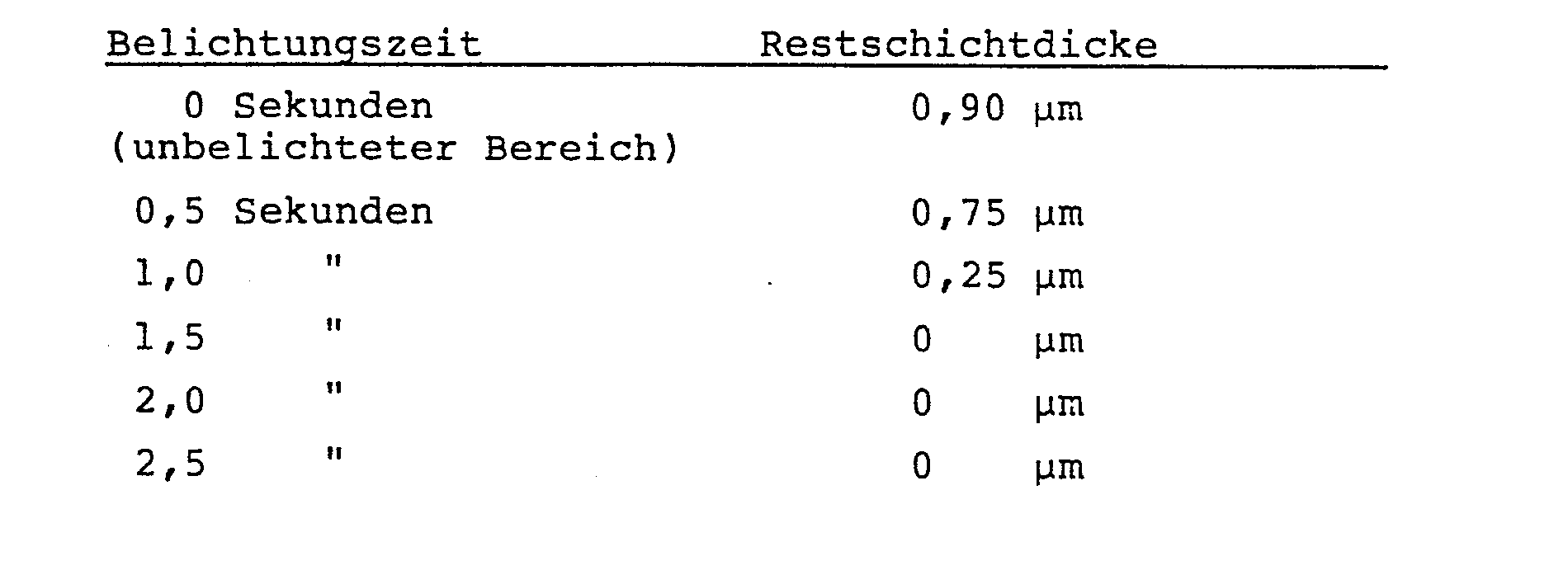
Danach werden die Wafer 60 Sekunden lang in dem Entwickler nach a) bei 22°C entwickelt. Nach der Entwicklung werden die erhaltenen Reliefstrukturen begutachtet und die verbleibende Restschichtdicke vermessen.The wafers are then developed in the developer according to a) at 22 ° C. for 60 seconds. After development, the relief structures obtained are examined and the remaining layer thickness is measured.
Folgende Restschichtdicken wurden in Abhängigkeit von der Belichtungszeit gefunden:

Eine rasterelektronenmikroskopische Auswertung der Strukturen im Fotolack zeigt, daß Muster mit einer Strukturbreite von 1 µm und darunter ab einer Belichtungszeit von 2 Sekunden sauber entwickelt und hoch aufgelöst sind, während bei Belichtungszeiten unter 2 Sekunden bzw. in den unbelichteten Bereichen ein Schichtabtrag von weniger als 5 % festzustellen ist. Die Reliefbilder zeigen glatte, ebene Oberflächen ohne Vertiefungen mit scharfen, steilen Kanten ohne Abrundungen oder Einschrägungen. Weder auf dem Resistbild noch auf dem freigelegten Substrat sind Ablagerungen von Verunreinigungen zu erkennen.A scanning electron microscope evaluation of the structures in the photoresist shows that patterns with a structure width of 1 µm and below are neatly developed and high-resolution from an exposure time of 2 seconds, while a layer removal of less than 5 in exposure times under 2 seconds or in the unexposed areas % can be determined. The relief images show smooth, flat surfaces without depressions with sharp, steep edges without roundings or bevels. Deposits of contaminants cannot be seen on the resist image or on the exposed substrate.

Die Anwendung analog zu Beispiel lb liefert gleichermaßen gute Ergebnisse.The application analogous to example lb gives equally good results.

Die Anwendung analog zu Beispiel lb liefert gleichermaßen gute Ergebnisse.The application analogous to example lb gives equally good results.
Wie in Beispiel la, jedoch mit 0,1 Gew.% (≙ 1000 ppm) des Tensides.As in Example la, but with 0.1% by weight (≙ 1000 ppm) of the surfactant.
Bei einer Entwicklung analog zu Beispiel lb sind selbst bei Belichtungszeiten von 10 Sekunden keine vollständig entwickelten Reliefstrukturen erhältlich.With a development analogous to Example 1b, even with exposure times of 10 seconds, no fully developed relief structures are available.
Wie in Beispiel la, jedoch ohne Tensid.As in example la, but without surfactant.
Die Reliefbilder zeigen ungleichmäßige Oberflächen und stark abgerundete bzw. eingeschrägte Übergänge in den Grenzbereichen zwischen Resist und freigelegtem Substrat.The relief images show uneven surfaces and strongly rounded or beveled transitions in the border areas between the resist and the exposed substrate.
Claims (4)
Applications Claiming Priority (2)
| Application Number | Priority Date | Filing Date | Title |
|---|---|---|---|
| DE3346979 | 1983-12-24 | ||
| DE19833346979 DE3346979A1 (en) | 1983-12-24 | 1983-12-24 | DEVELOPER FOR POSITIVE PHOTO RESISTS |
Publications (2)
| Publication Number | Publication Date |
|---|---|
| EP0146834A2 true EP0146834A2 (en) | 1985-07-03 |
| EP0146834A3 EP0146834A3 (en) | 1986-08-20 |
Family
ID=6218066
Family Applications (1)
| Application Number | Title | Priority Date | Filing Date |
|---|---|---|---|
| EP84114722A Withdrawn EP0146834A3 (en) | 1983-12-24 | 1984-12-04 | Positive photoresist developer |
Country Status (5)
| Country | Link |
|---|---|
| US (1) | US4576903A (en) |
| EP (1) | EP0146834A3 (en) |
| JP (1) | JPS60158442A (en) |
| KR (1) | KR850004661A (en) |
| DE (1) | DE3346979A1 (en) |
Cited By (2)
| Publication number | Priority date | Publication date | Assignee | Title |
|---|---|---|---|---|
| EP0364895A1 (en) * | 1988-10-20 | 1990-04-25 | Mitsubishi Gas Chemical Company, Inc. | Positive type photoresist developer |
| US5175078A (en) * | 1988-10-20 | 1992-12-29 | Mitsubishi Gas Chemical Company, Inc. | Positive type photoresist developer |
Families Citing this family (24)
| Publication number | Priority date | Publication date | Assignee | Title |
|---|---|---|---|---|
| DE3427556C1 (en) * | 1984-07-26 | 1986-01-02 | Merck Patent Gmbh, 6100 Darmstadt | Process for the production of photoresist relief structures with an overhang character |
| DE3580827D1 (en) * | 1984-10-09 | 1991-01-17 | Hoechst Japan K K | METHOD FOR DEVELOPING AND DE-COATING PHOTORESIS LAYERS WITH QUATERIAL AMMOMIUM COMPOUNDS. |
| JPH063549B2 (en) * | 1984-12-25 | 1994-01-12 | 株式会社東芝 | Positive photoresist developer composition |
| JPH0638396B2 (en) * | 1985-02-04 | 1994-05-18 | ソニー株式会社 | Method of developing positive type photoresist |
| JPS62175738A (en) * | 1986-01-30 | 1987-08-01 | Japan Synthetic Rubber Co Ltd | Liquid developer |
| JPH0638159B2 (en) * | 1986-07-18 | 1994-05-18 | 東京応化工業株式会社 | Developer for positive photoresist |
| GB8628613D0 (en) * | 1986-11-29 | 1987-01-07 | Horsell Graphic Ind Ltd | Developing fluid for lithographic plates |
| JP2542903B2 (en) * | 1988-04-22 | 1996-10-09 | 富士写真フイルム株式会社 | Developer composition |
| DE3827567A1 (en) * | 1988-08-13 | 1990-02-22 | Basf Ag | WAITER DEVELOPER SOLUTION FOR POSITIVELY WORKING PHOTORE RESTS |
| US5278030A (en) * | 1988-10-24 | 1994-01-11 | Du Pont-Howson Limited | Developer solution comprising ethyl hexyl sulphate, a surfactant, an alkaline material and having a pH of not less than 12 |
| US5252436A (en) * | 1989-12-15 | 1993-10-12 | Basf Aktiengesellschaft | Process for developing a positive-working photoresist containing poly(p-hydroxystyrene) and sulfonium salt with an aqueous developer containing basic organic compounds |
| US5543268A (en) * | 1992-05-14 | 1996-08-06 | Tokyo Ohka Kogyo Co., Ltd. | Developer solution for actinic ray-sensitive resist |
| US5329655A (en) * | 1993-05-18 | 1994-07-19 | Dean Garner | Slidable hospital sheet for turning patients |
| EP0732628A1 (en) * | 1995-03-07 | 1996-09-18 | Minnesota Mining And Manufacturing Company | Aqueous alkaline solution for developing offset printing plate |
| US5897985A (en) * | 1996-10-11 | 1999-04-27 | Kodak Polychrome Graphics, Llc | Potassium silicate developing composition and method of use to process lithographic printing plates |
| US5766826A (en) * | 1996-10-11 | 1998-06-16 | Eastman Kodak Company | Alkaline developing composition and method of use to process lithographic printing plates |
| US6083662A (en) * | 1997-05-30 | 2000-07-04 | Kodak Polychrome Graphics Llc | Methods of imaging and printing with a positive-working infrared radiation sensitive printing plate |
| US5811221A (en) * | 1997-05-30 | 1998-09-22 | Kodak Polychrome Graphics, Llc | Alkaline developing composition and method of use to process lithographic printing plates |
| GB9723026D0 (en) * | 1997-11-01 | 1998-01-07 | Du Pont Uk | Improvements in or relating to the processing of lithographic printing plate precursors |
| GB9723025D0 (en) * | 1997-11-01 | 1998-01-07 | Du Pont Uk | Improvements in or relating to the processing of lithographic printing plate precursors |
| US6248171B1 (en) * | 1998-09-17 | 2001-06-19 | Silicon Valley Group, Inc. | Yield and line width performance for liquid polymers and other materials |
| JP2002351094A (en) * | 2001-05-22 | 2002-12-04 | Fuji Photo Film Co Ltd | Developer composition and image forming method |
| JP4230130B2 (en) * | 2001-07-04 | 2009-02-25 | 富士フイルム株式会社 | Photosensitive lithographic printing plate developer and lithographic printing plate making method |
| US8247029B2 (en) * | 2008-06-17 | 2012-08-21 | Tdk Corporation | Method for forming micropattern |
Family Cites Families (15)
| Publication number | Priority date | Publication date | Assignee | Title |
|---|---|---|---|---|
| DE1572153B2 (en) * | 1966-06-27 | 1971-07-22 | E I Du Pont de Nemours and Co , Wilmington, Del (V St A ) | PHOTOPOLYMERIZABLE RECORDING MATERIAL |
| US3586504A (en) * | 1969-10-24 | 1971-06-22 | Eastman Kodak Co | Photoresist developers and methods |
| JPS5032643B2 (en) * | 1971-10-04 | 1975-10-23 | ||
| US4147545A (en) * | 1972-11-02 | 1979-04-03 | Polychrome Corporation | Photolithographic developing composition with organic lithium compound |
| DE2530502C2 (en) * | 1974-07-22 | 1985-07-18 | American Hoechst Corp., Bridgewater, N.J. | Process for the simultaneous development and preservation of printing plates as well as a suitable treatment solution therefor |
| JPS5119536A (en) * | 1974-08-09 | 1976-02-16 | Bunshodo Co Ltd | Jiazofukushaniokeru aminkeigenzoeki |
| US4001133A (en) * | 1974-11-04 | 1977-01-04 | Basf Wyandotte Corporation | Method of washing glassware and inhibited cleaning solution and additive composition useful therein |
| PL95558B1 (en) * | 1975-01-16 | 1978-06-20 | DEVICE FOR PROCESSING OFFSET LAYERS OF OQUINONE COPIES | |
| DD123398A1 (en) * | 1975-08-15 | 1976-12-12 | ||
| JPS608494B2 (en) * | 1978-03-01 | 1985-03-04 | 富士通株式会社 | Formation method of positive resist image |
| JPS5595946A (en) * | 1979-01-16 | 1980-07-21 | Mitsubishi Chem Ind Ltd | Developer for o-quinone diazide type photosensitive material |
| US4212902A (en) * | 1979-03-09 | 1980-07-15 | Zenith Radio Corporation | Method for aluminizing image display faceplates |
| US4263392A (en) * | 1979-06-01 | 1981-04-21 | Richardson Graphics Company | Ultra high speed presensitized lithographic plates |
| US4308340A (en) * | 1980-08-08 | 1981-12-29 | American Hoechst Corporation | Aqueous 2-propoxyethanol containing processing composition for lithographic printing plates |
| US4374920A (en) * | 1981-07-27 | 1983-02-22 | American Hoechst Corporation | Positive developer containing non-ionic surfactants |
-
1983
- 1983-12-24 DE DE19833346979 patent/DE3346979A1/en not_active Ceased
-
1984
- 1984-12-04 EP EP84114722A patent/EP0146834A3/en not_active Withdrawn
- 1984-12-14 KR KR1019840008290A patent/KR850004661A/en not_active Withdrawn
- 1984-12-21 US US06/685,085 patent/US4576903A/en not_active Expired - Fee Related
- 1984-12-24 JP JP59271073A patent/JPS60158442A/en active Pending
Cited By (2)
| Publication number | Priority date | Publication date | Assignee | Title |
|---|---|---|---|---|
| EP0364895A1 (en) * | 1988-10-20 | 1990-04-25 | Mitsubishi Gas Chemical Company, Inc. | Positive type photoresist developer |
| US5175078A (en) * | 1988-10-20 | 1992-12-29 | Mitsubishi Gas Chemical Company, Inc. | Positive type photoresist developer |
Also Published As
| Publication number | Publication date |
|---|---|
| EP0146834A3 (en) | 1986-08-20 |
| JPS60158442A (en) | 1985-08-19 |
| KR850004661A (en) | 1985-07-25 |
| US4576903A (en) | 1986-03-18 |
| DE3346979A1 (en) | 1985-07-04 |
Similar Documents
| Publication | Publication Date | Title |
|---|---|---|
| EP0146834A2 (en) | Positive photoresist developer | |
| EP0000702B1 (en) | Process for forming a flow-resistant resist mask of radioation-sensitive material | |
| EP0002795B1 (en) | Process for the fabrication of masks for lithographic processes using a photoresist | |
| EP0164620B1 (en) | Positively acting light-sensitive coating solution | |
| DE69313132T2 (en) | METALION REDUCTION IN ANTI-REFLECTIVE UNDERLAYERS FOR PHOTORESIST | |
| EP0042562B1 (en) | Positive-working radiation-sensitive composition | |
| DE2460988C2 (en) | A method of depositing a pattern from a thin film on an inorganic substrate | |
| EP0164083B1 (en) | Positively acting light-sensitive coating solution | |
| DE2447225C2 (en) | Process for peeling off positive photoresist | |
| DE2655455C2 (en) | Method for producing a mask and lacquer structure for use in the method | |
| DE2754396A1 (en) | METHOD OF MANUFACTURING THIN FILM PATTERNS | |
| DE3239613A1 (en) | LIGHT SENSITIVE COMPOSITIONS | |
| EP0212482B1 (en) | Process for obtaining negative images from positive photoresists | |
| DE2312499A1 (en) | DIAZOCHINON-SILOXANE AND USE OF THE SAME FOR PHOTO LACQUERS AND LIGHT-SENSITIVE OBJECTS | |
| DE3621376A1 (en) | RADIATION-SENSITIVE RECORDING MATERIAL | |
| EP0220645B1 (en) | Photosensitive positive composition and photoresist material prepared therewith | |
| EP0355015B1 (en) | Process for developing positively acting photoresists | |
| EP0008394A1 (en) | Process for developing exposed light-sensitive printing plates containing o-naphthoquinone diazides | |
| DE2521727A1 (en) | METHOD FOR MANUFACTURING A RESIST IMAGE | |
| DE69323200T2 (en) | DIAZONAPHTHOCHINONSULFONIC ACID ESTERS OF HEXAHYDROXYBENZOPHENONE AS SENSITIZERS AND POSITIVE-PHOTORESISTS BASED ON THEM | |
| DE3427556C1 (en) | Process for the production of photoresist relief structures with an overhang character | |
| EP0195315B1 (en) | Process for the production of photoresist patterns | |
| DE3421160A1 (en) | Positive-working radiation-sensitive coating solution | |
| DE3337303C2 (en) | Process for the photolithographic production of fine resist patterns and photosensitive mixtures usable therefor | |
| EP0508267B1 (en) | Radiation-sensitive composition with 1,2-naphthoquinone-2-dazide-sulfonic acid esters and recording material produced therewith |
Legal Events
| Date | Code | Title | Description |
|---|---|---|---|
| PUAI | Public reference made under article 153(3) epc to a published international application that has entered the european phase |
Free format text: ORIGINAL CODE: 0009012 |
|
| AK | Designated contracting states |
Designated state(s): AT CH DE FR GB IT LI NL SE |
|
| PUAL | Search report despatched |
Free format text: ORIGINAL CODE: 0009013 |
|
| AK | Designated contracting states |
Kind code of ref document: A3 Designated state(s): AT CH DE FR GB IT LI NL SE |
|
| 17P | Request for examination filed |
Effective date: 19861223 |
|
| 17Q | First examination report despatched |
Effective date: 19880304 |
|
| STAA | Information on the status of an ep patent application or granted ep patent |
Free format text: STATUS: THE APPLICATION HAS BEEN WITHDRAWN |
|
| 18W | Application withdrawn |
Withdrawal date: 19880728 |
|
| RIN1 | Information on inventor provided before grant (corrected) |
Inventor name: MARQUARD, KURT, DR. Inventor name: MERREM, HANS-JOACHIM, DR. Inventor name: THIEL, KLAUS-PETER Inventor name: SINDLINGER, RAIMUND Inventor name: BARON, WINFRIED |