EP0147073A1 - Circuit de réduction du bruit pour un signal vidéo - Google Patents
Circuit de réduction du bruit pour un signal vidéo Download PDFInfo
- Publication number
- EP0147073A1 EP0147073A1 EP84308247A EP84308247A EP0147073A1 EP 0147073 A1 EP0147073 A1 EP 0147073A1 EP 84308247 A EP84308247 A EP 84308247A EP 84308247 A EP84308247 A EP 84308247A EP 0147073 A1 EP0147073 A1 EP 0147073A1
- Authority
- EP
- European Patent Office
- Prior art keywords
- circuit
- video signal
- output
- signal
- input
- Prior art date
- Legal status (The legal status is an assumption and is not a legal conclusion. Google has not performed a legal analysis and makes no representation as to the accuracy of the status listed.)
- Granted
Links
- 230000009467 reduction Effects 0.000 title claims abstract description 96
- 230000000295 complement effect Effects 0.000 claims abstract description 8
- 230000001934 delay Effects 0.000 claims abstract description 6
- 238000001914 filtration Methods 0.000 claims 7
- 230000006866 deterioration Effects 0.000 description 16
- 239000003990 capacitor Substances 0.000 description 13
- 238000010276 construction Methods 0.000 description 11
- 238000010586 diagram Methods 0.000 description 8
- 230000006872 improvement Effects 0.000 description 7
- 230000009897 systematic effect Effects 0.000 description 7
- 230000003111 delayed effect Effects 0.000 description 5
- 230000004048 modification Effects 0.000 description 5
- 238000012986 modification Methods 0.000 description 5
- 230000008859 change Effects 0.000 description 3
- 230000001603 reducing effect Effects 0.000 description 3
- 230000002238 attenuated effect Effects 0.000 description 2
- 238000001228 spectrum Methods 0.000 description 2
- 230000003321 amplification Effects 0.000 description 1
- 238000013459 approach Methods 0.000 description 1
- 230000008878 coupling Effects 0.000 description 1
- 238000010168 coupling process Methods 0.000 description 1
- 238000005859 coupling reaction Methods 0.000 description 1
- 230000007423 decrease Effects 0.000 description 1
- 230000001419 dependent effect Effects 0.000 description 1
- 230000002542 deteriorative effect Effects 0.000 description 1
- 229910052732 germanium Inorganic materials 0.000 description 1
- GNPVGFCGXDBREM-UHFFFAOYSA-N germanium atom Chemical compound [Ge] GNPVGFCGXDBREM-UHFFFAOYSA-N 0.000 description 1
- 238000003199 nucleic acid amplification method Methods 0.000 description 1
Images



Classifications
-
- H—ELECTRICITY
- H04—ELECTRIC COMMUNICATION TECHNIQUE
- H04N—PICTORIAL COMMUNICATION, e.g. TELEVISION
- H04N5/00—Details of television systems
- H04N5/14—Picture signal circuitry for video frequency region
- H04N5/21—Circuitry for suppressing or minimising disturbance, e.g. moiré or halo
Definitions
- the present invention generally relates to noise reduction circuits for video signals, and more particularly to a noise reduction circuit which comprises a filter circuit within a feedback loop of a feedback type comb filter and effectively reduces noise within an input video signal so as to improve the picture quality, by varying the feedback ratio responsive to the frequency.
- a noise reduction circuit is provided in a luminance signal reproducing system of a helical scan type magnetic recording and/or reproducing apparatus (video tape recorder or VTR), for example, so as to reduce noise within a reproduced luminance signal after a frequency demodulation.
- a first conventional noise reduction circuit the reproduced luminance signal which is reproduced from a magnetic tape and is demodulated in a frequency demodulator, is applied to an input terminal and is passed through a highpass filter so as to obtain only a frequency component of over 1 MHz, for example.
- An output signal of the highpass filter is passed through a limiter and a coefficient multiplier, and is supplied to a -subtracting circuit.
- the subtracting circuit subtracts the output signal of the coefficient multiplier from the video signal (reproduced luminance signal, for example) applied to the input terminal.
- the noise which is visually conspicuous to the human eye is generally concentrated in a low-level part of the high-frequency component. Hence, a video signal in which the visually conspicuous noise is eliminated, is produced from the subtracting circuit and is obtained through an output terminal.
- the video signal (reproduced luminance signal, for example) which is applied to an input terminal, is supplied to a 1H delay circuit wherein the video signal is delayed by a delay time of lH, where H represents one horizontal scanning period.
- An output delayed video signal is supplied to a first subtracting circuit.
- the first subtracting circuit subtracts the output delayed video signal of the 1H delay circuit from the video signal applied to the input terminal.
- information contents which are separated by an interval of lH are extremely similar to each other, and the so-called vertical correlation (line correlation) exists, as is well known. However, the vertical correlation does not exist for the noise.
- a signal made up of the noise and a video signal component having no vertical correlation is obtained from the first subtracting circuit.
- the output signal of the first subtracting circuit is subjected to an amplitude limitation in a limiter which has a limiting level in the range of a peak-to-peak value of the noise.
- An output signal of the limiter is supplied to a second subtracting circuit which subtracts the output signal of the limiter from the video signal applied to the input terminal. Consequently; a video signal in which the noise is greatly reduced, is produced from the second subtracting circuit and is obtained through an output terminal.
- a third conventional noise'reduction circuit comprising a feedback type comb filter.
- This third conventional noise reduction circuit will be described later in detail in conjunction with a drawing.
- a video signal (reproduced luminance signal, for example) is applied to an input terminal, and is supplied to the feedback type comb filter which eliminates the noise and obtains a video signal component having the vertical correlation.
- An output signal of the feedback type comb filter is supplied to a subtracting circuit which subtracts the output signal of the feedback type comb filter from the video signal applied to the input terminal, so as to obtain a signal made up of the noise included within the video signal and a video signal component having no vertical correlation.
- the output signal of the subtracting circuit is passed through a lowpass filter which obtains only a low-frequency component of the output signal of the subtracting circuit.
- the output signal of the feedback type comb filter has a predetermined characteristic after being passed through an equalizer circuit.
- the output signal of the lowpass filter and an output signal of the equalizer circuit are added in an adding circuit. As a result, a signal in which the noise is eliminated, is produced from the adding circuit and is obtained through an output terminal.
- the frequency characteristic of the third conventional noise reduction circuit is flat in a frequency band under a cutoff frequency f of the lowpass filter, but has a comb filter characteristic in a frequency band over the cutoff frequency f so as to pass frequency components which are natural number multiples of a horizontal scanning frequency f H .
- the third conventional noise reduction circuit it is possible to eliminate the noise in the high-frequency band over the cutoff frequency f. Further, it is possible to prevent deterioration in the vertical resolution which is visually conspicuous in the low-frequency band under the cutoff frequency f .
- the video signal applied to the input terminal has an edge of a large amplitude
- a high-frequency component of the edge is obtained from the highpass filter in the first conventional noise reduction circuit described before.
- the video signal and the noise in the vicinity of the edge are eliminated by the amplitude limitation performed in the limiter.
- a video signal in which the edge noise still remains in the vicinity of the edge where the amplitude limitation is performed in the limiter is produced from the subtracting circuit and is obtained through the output terminal.
- the signal-to noise (S/N) ratio of the reproduced video signal is poor because the track width is narrow and the relative linear speed between the magnetic tape and a head is slow.
- the crosstalk from adjacent tracks is large, and the edge noise is visually conspicuous in the reproduced picture. For this reason, the S/N ratio cannot be improved sufficiently according to the first conventional noise reduction circuit.
- the noise is also distributed in the low-frequency band under 1 MHz. Since the first conventional noise reduction circuit is only effective with respect to the noise over the cutoff frequency of the highpass filter, it is also impossible to obtain the noise reducing effect with respect to the noise in the low-frequency band at parts other than the edge of the video signal.
- the second conventional noise reduction circuit is superior compared to the first conventional noise reduction circuit in that the second conventional noise reduction circuit can eliminate the edge noise and improve the S/N ratio.
- the S/N ratio can be improved theoretically by 3 dB, the S/N ratio can only be improved by approximately 1.5 dB to 2.0 dB in actual practice.
- the second conventional noise reduction circuit has a comb filter characteristic which passes frequencies which are natural number multiples of the horizontal scanning frequency f H to the same extent throughout the entire frequency band. As a result, the vertical resolution becomes deteriorated, and there is a problem in that the deterioration in the vertical resolution is visually conspicuous especially in the low-frequency band.
- the third conventional noise reduction circuit is advantageous in that it is possible to reduce the edge noise described before.
- the low-frequency noise in the range of 1 MHz
- the cutoff frequency f of the lowpass filter cannot be reduced in the low-frequency band under the cutoff frequency f of the lowpass filter.
- a coefficient of a coefficient multiplier within the feedback type comb filter must be set to a large value in order to obtain a desired S/N ratio improvement factor which is greater than the S/N ratio improvement factor obtainable in the second conventional noise reduction circuit.
- the comb filter characteristic becomes sharp, and the vertical resolution is greatly deteriorated in the frequency band over the cutoff frequency f of the lowpass filter.
- the deterioration in the vertical resolution is visually conspicuous in a frequency range of 1 MHz to 2 MHz.
- the cutoff frequency f of the lowpass filter must inevitably be set to a frequency in the range of 2 MHz to 3 MHz, and it is virtually impossible to improve the S/N ratio in the low-frequency band by the desired improvement factor so as to reduce the low-frequency noise which are visually conspicuous especially in the reproduced picture obtained in the VTR.
- Another and more specific object of the present invention is to provide a noise reduction circuit for a video signal, which comprises a highpass filter or a bandpass filter within a feedback loop of a feedback type comb filter, and passes an output signal of the feedback type comb filter through an equalizer circuit having a predetermined characteristic, so that an output video signal of the equalizer circuit is obtained through an output terminal.
- the noise reduction circuit of the present invention it is possible to reduce the low-frequency noise which is visually conspicuous especially in the reproduced picture obtained in the VTR and improve the S/N ratio to such an extent that the vertical resolution is hardly deteriorated.
- it is possible to greatly improve the S/N ratio in the high-frequency band that is, by approximately 6 dB to 10 dB.
- Still another object of the present invention is to provide a noise reduction circuit for a video signal, in which the output video signal of the equalizer circuit is supplied to an adding circuit through a subtracting circuit and a clipping circuit, and is also supplied directly to the adding circuit.
- the noise reduction circuit of the present invention it is possible to obtain a variable frequency characteristic which is in accordance with the rate of the vertical correlation in the video signal. With respect to a video signal having a strong vertical correlation, it is possible to obtain from the adding circuit a video signal in which the noise is greatly reduced by the comb filter characteristic.
- the filter characteristic is changed so as to pass the entire frequency band, and it is possible to obtain from the adding circuit a video signal having no deterioration in the vertical resolution.
- a further object of the present invention is to provide a noise reduction circuit for a video signal, in which the output video signal of the equalizer circuit is supplied to a filter circuit which separates the video signal into a signal in a high-frequency band and a signal in a low-frequency band.
- the output signal of the filter circuit in the high-frequency band is passed through a clipping circuit and is added with the output signal of the filter circuit in the low-frequency band.
- a signal which is obtained by this addition is added with the output video signal of the feedback type comb filter, and is obtained through the output terminal.
- the vertical resolution is not deteriorated in a low-frequency band under a cutoff frequency of the filter circuit.
- the vertical correlation exists in the video signal, it is possible to reduce the low-frequency noise which is visually conspicuous especially in the reproduced picture obtained in the VTR and improve the S/N ratio to such an extent that the vertical resolution is hardly deteriorated.
- the operation of improving the S/N ratio is stopped, so as to accurately produce a video signal having virtually no deterioration in the vertical resolution.
- Another object of the present invention is to provide a noise reduction circuit in which an equalizer circuit having an open loop construction and comprising a limiter and a filter circuit in a non-feedback path thereof, is coupled to an output side of a feedback type comb filter having a limiter and a filter circuit in a feedback path thereof.
- the noise reduction circuit of the present invention it is possible to perform an optimum noise reducing operation depending on the amplitude of the input video signal, while preventing deterioration in the vertical resolution. Further, it is possible to reduce the edge noise in which the vertical correlation exists, and improve the input pulse versus output pulse characteristic with respect to an input pulse signal. Moreover, the noise which cannot be reduced, is greatly suppressed in the high-frequency range by the comb filter.
- the phenomenon in which trails are formed in the horizontal direction of the picture can be made less visually conspicuous.
- the S/N ratio can be improved considerably in the feedback type comb filter for the high-frequency range with respect to the input video signal having a small level, the attenuation need not be large in the equalizer circuit in this case. Accordingly, the frequency characteristic with respect to the input video signal having a small level is improved, and it is possible to clearly reproduce the contours of images in the reproduced picture.
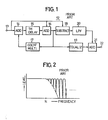
- a noise reduction circuit 12 shown in FIG.1 is the third conventional noise reduction circuit described before.
- an input video signal (a reproduced luminance signal, for example) is applied to an input terminal 13, and is supplied to a 1H delay circuit 15 through an adding circuit 14, where H represents one horizontal scanning period of the input video signal.
- An output signal of the adding circuit 14 which is delayed by a delay time of 1H in the 1H delay circuit 15, is supplied to an adding circuit 16.
- the adding circuit 16 adds the output signal of the lH delay circuit 15 and the input video signal applied to the input terminal 13, and produces a video signal component which has the vertical correlation and is reduced of the noise.
- the output video signal component of the adding circuit 16 is supplied to a coefficient multiplier 17 which multiplies a coefficient to the video signal component, and output signal of the coefficient multiplier 17 is fed back to the adding circuit 14.
- the adding circuit 14, the 1H delay circuit 15, the adding circuit 16, and the coefficient multiplier 17, constitute a feedback type comb filter.
- the feedback type comb filter has a comb filter characteristic in which center frequencies of pass bands are even number multiples of 1/2 the horizontal scanning frequency f H' and center frequencies of attenuation bands are odd number multiples of f H / 2.
- An output signal of the feedback type comb filter that is, the output signal of the adding circuit 16 is subtracted from the input video signal applied to the input terminal 13, in a subtracting circuit 18.
- a signal made up of the noise within the input video signal and a video signal component having no vertical correlation is obtained from the subtracting circuit 18.
- the output signal of the subtracting circuit 18 is supplied to a lowpass filter 20 having a cutoff frequency f. Only a low-frequency component is obtained from the lowpass filter 20, and this low-frequency component is supplied to an adding circuit 21.
- the output video signal of the adding circuit 16 is supplied to an equalizer circuit 19, and a signal having a predetermined characteristic is obtained from the equalizer circuit 19.
- the output signal of the equalizer circuit 19 is supplied to the adding circuit 21 and is added with the output low-frequency component of the lowpass filter 20.
- An output signal of the adding circuit 21 is obtained through an output terminal 22.
- the conventional noise reduction circuit shown in FIG.1 has a frequency characteristic shown in FIG.2.
- the conventional noise reduction circuit has a frequency characteristic which is flat in a frequency band under the cutoff frequency f of the lowpass filter 20, and has a feedback type comb filter characteristic in which center frequencies of pass bands are natural number multiples of the horizontal scanning frequency f H .
- the conventional noise reduction circuit shown in FIG.l it is possible to reduce the noise in the high-frequency band over the cutoff frequency f , and it is possible to prevent deterioration in the vertical resolution which is visually conspicuous in the low-frequency band under the cutoff frequency f .
- the cutoff frequency f c of the lowpass filter 20 is inevitably selected to a frequency in the range of 2 MHz to 3 MHz.
- the frequency characteristic shown in FIG.2 there is a problem in that it is impossible to reduce the low-frequency noise (in the range of 1 MHz) which is visually conspicuous especially in the reproduced picture obtained in the VTR.
- FIG.3 shows a first embodiment of a noise reduction circuit 30 according to the present invention.
- an input video signal including noise is applied to an input terminal 31.
- the input video signal is a reproduced luminance signal which is obtained by reproducing a frequency modulated luminance signal from a recording medium and then passing the reproduced frequency modulated luminance signal through a de-emphasis circuit or the like.
- the input video signal is passed through an adding circuit 32 and a lH delay circuit 33, and is supplied to an adding circuit 34.
- the input video signal is also supplied directly to the adding circuit 34.
- An output video signal of the adding circuit 34 is supplied to a highpass filter 35 which comprises a capacitor C l and a resistor R Z .
- the highpass filter 35 attenuates a low-frequency component under a cutoff frequency f c12 ' and filters a high-frequency component.
- the output high-frequency component of the highpass filter 35 is supplied to a coefficient multiplier 36 which multiplies a coefficient k to the high-frequency component.
- An output signal of the coefficient multiplier 36 is supplied to the adding circuit 32 and is added with the input video signal, and the output signal of the adding circuit 32 is supplied to the 1H delay circuit 33.
- the adding circuits 32 and 34, the 1H delay circuit 33, the highpass filter 35, and the coefficient multiplier 36, constitute a feedback type comb filter 37 in which the output video signal of the 1H delay circuit 33 is fed back to the input thereof.
- a video signal having a frequency characteristic in which the center frequencies of the pass bands are even number multiples of f H /2 and the center frequencies of the attenuation bands are odd number multiples of f H /2, is obtained from the adding circuit 34.
- the feedback ratio of the high-frequency component over the cutoff frequency f cl2 is large, because the highpass filter 35 is provided in the feedback path which includes the coefficient multiplier 36 and extends from the output of the 1H delay circuit 34 to the input of the 1H delay circuit 34.
- the value of the coefficient k with respect to the high-frequency component essentially becomes larger compared to the value of the coefficient k with respect to the low-frequency component.
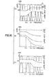
- the frequency characteristic obtained at the output of the adding circuit 34 is a comb filter characteristic in which the levels of the pass bands become larger and the pass bands become sharper (narrower) from the vicinity of the cutoff frequency f cl2 toward the higher frequencies, as may be seen from a feedback type comb filter characteristic shown in FIG.4(A).
- the highpass filter 35 may be provided between the output of the coefficient multiplier 36 and the input of the adding circuit 32.
- the envelope characteristic I is obtained by connecting peak levels of the pass bands in the frequency characteristic of the feedback type comb filter 37.
- the coefficient k of the coefficient multiplier 36 is greater than zero and less than one
- the feedback ratio obtained by the highpass filter 35 is represented by ⁇
- the input signal voltage applied to the input terminal 31 is represented by e i
- the output signal voltage of the adding circuit 34 is represented by e o
- the transfer function of the feedback type comb filter 37 can be described by the following equation (1), when it is assumed that a perfect vertical correlation exists in the signal.
- C 1 ⁇ R 1 T because the highpass filter 35 comprises the capacitor C I and the resistor R 1
- equation (2) can be obtained, where w represents the angular frequency of the input signal.
- the equation (3) describes the envelope characteristic I in the frequency characteristic of the feedback type comb filter 37.
- the level difference between the frequencies f c11 and f c12 can be described by 201og[1/(1 - k)] dB.
- the feedback type comb filter 37 has the frequency characteristic in which the center frequencies of the pass bands are even number multiples of 1/2 the horizontal scanning frequency f H , and the pass bands are sharper (narrower) in the higher frequencies compared to the lower frequencies.
- a video signal which is obtained from the feedback type comb filter 37 is supplied to an equalizer circuit 38 which comprises resistors R 2 and R 3 and a capacitor C 2 , and a signal having a predetermined characteristic is obtained from the equalizer circuit 38.
- the output signal of the equalizer circuit 38 is obtained through an output terminal 39.
- the equalizer circuit 38 has a frequency characteristic complementary to the envelope characteristic I in the frequency characteristic of the feedback type comb filter 37.
- the circuit construction of the equalizer circuit 38 becomes as shown in FIG.3.
- the frequency characteristic of the equalizer circuit 38 is flat in the frequency band under a first cutoff frequency f c12 ' flat in the frequency band over a second cutoff frequency f cll' and slopes at a rate of -6 dB/oct as the frequency increases from the first cutoff frequency f c12 to the second cutoff frequency f cll .
- the first cutoff frequency f c12 is determined by a product of the capacitance of the capacitor C 2 and a sum of the resistances of the resistors R 2 and R 3 .
- the second cutoff frequency f cll is determined by a product of the capacitance of the capacitor C 2 and the resistance of the resistor R 3 .
- the constants of the circuit elements in the highpass filter 35 and the equalizer circuit 38 are thus selected as follows.
- the frequency characteristic of the noise reduction circuit 30 which exists between the input terminal 31 and the output terminal 39, is a sum of the frequency characteristic of the feedback type comb filter 37 shown in FIG.4(A) and the frequency characteristic of the equalizer circuit 38 shown in FIG.4(B). As a result, the frequency characteristic of the noise reduction circuit 30 becomes as shown in FIG.4(C).
- the noise reduction circuit 30 has a frequency characteristic in which the pass bands and the attenuation bands are the same as the pass bands and the attenuation bands in the frequency characteristic of the feedback type comb filter 37 throughout the entire frequency band, the pass bands gradually become sharper (narrower) toward the higher frequencies in the frequency band between the frequencies f cl2 and f c11 , and the pass bands are sharpest (narrowest) in the high-frequency band over the frequency f cll .
- the envelope characteristic in the frequency characteristic of the noise reduction circuit 30, that is, a peak frequency characteristic in the comb filter characteristic, is substantially flat throughout the entire frequency band as indicated by a phantom line II in FIG.4(C).
- coefficients l, m, and n are natural numbers, and satisfy a relation Q ⁇ m ⁇ n.
- the same coefficients are used in FIGS.6(A) through 6(E) which will be described later on.
- the noise reduction circuit 30 blocks the frequency components having frequencies which are odd number multiples of 1/2 the horizontal scanning frequency f H . As a result, it is possible to reduce the noise which is mixed in the input signal (reproduced luminance signal) approximately throughout the entire frequency band. Because the noise reduction circuit 30 shows a narrow comb filter characteristic especially toward the high-frequency band, it is possible to greatly reduce the noise in the high-frequency band.
- the cutoff frequency f cl2 of the highpass filter 35 is in the range of 800 kHz, for example, and is sufficiently low compared to the cutoff frequency f of the lowpass filter 20 within the conventional noise reduction circuit 12 shown in FIG.l.
- the pass bands are wider in the low-frequency band under the frequency f c12 , and the pass bands are narrower in the high-frequency band over the frequency f c11 .
- S/N ratio improvement factor which is approximately in the same range as the S/N ratio improvement factor obtainable in the conventional noise reduction circuit 12 shown in FIG.l.
- FIG.5 a noise reduction circuit 40 shown in F IG.5
- the output video signal of the equalizer circuit 38 is supplied to a subtracting circuit 41 which subtracts the output video signal of the equalizer circuit 38 from the input video signal obtained through the input terminal 31.
- a frequency characteristic shown in FIG.6(C) is obtained at the output of the subtracting circuit 41.
- This frequency characteristic is obtained by subtracting the frequency characteristic shown in FIG.6(B) (identical to the frequency characteristic shown in FIG.4(C)) which is obtained at the output of the equalizer circuit 38, from a frequency characteristic which is flat throughout the entire frequency band.
- the center frequencies of the pass bands are odd number multiples of f H /2
- the center frequencies of the attenuation bands are even number multiples of f H /2
- the pass band characteristic in the high-frequency band over the frequency f cll is flat compared to the pass band characteristic in the low-frequency band under the frequency fc12.
- the center frequencies of the pass bands and the center frequencies of the attenuation bands in the frequency characteristic shown in FIG.6(C) which is obtained at the output of the subtracting circuit 41 respectively correspond to the center frequencies of the attenuation bands and the center frequencies of the pass bands in the frequency characteristic shown in FIG.6(A) which is obtained at the output of the comb filter 37 and in the frequency characteristic shown in FIG.6(B) which is obtained at the output of the equalizer circuit 38.
- the output signal of the subtracting circuit 41 having the frequency characteristic shown in FIG.6(C), is made up of the noise included within the input video signal (reproduced luminance signal) and the video signal component having no vertical correlation.
- This output signal of the subtracting circuit 41 is supplied to a clipping circuit 42.
- the clipping level of the clipping circuit 42 is selected in the range of a peak-to-peak level of the noise within the output signal of the subtracting circuit 41.
- the clipping circuit 42 has a known construction, and is designed to block a signal having a level which is smaller than the clipping level and to pass a signal having a level which is larger than the clipping level.
- An output signal of the clipping circuit 42 is supplied to an adding circuit 43, and is added with the output video signal of the equalizer circuit 38.
- An output signal of the adding circuit 43 is obtained through an output terminal 44.
- the level of the output signal of the subtracting circuit 41 is smaller than the clipping level of the clipping circuit 42, and no output is obtained from the clipping circuit 42. Accordingly, a video signal having a frequency characteristic shown in FIG.6(D) (identical to the frequency characteristic shown in FIG.6(B) which is obtained at the output of the equalizer circuit 6(B)), is obtained through the output terminal 44.
- the video signal component having no vertical correlation is included within the input video signal to a large extent.
- the level of the video signal component which has no vertical correlation and is obtained from the subtracting circuit 41 is larger than the clipping level of the clipping circuit 42.
- the adding circuit 43 adds the output signal of the clipping circuit 42 and the output signal of the equalizer circuit 38, a video signal having a frequency characteristic shown in FIG.6(E) is obtained from the adding circuit 43.
- This frequency characteristic shown in FIG.6(E) is obtained by adding the frequency characteristics shown in FIGS.6(B) and 6(C), and is substantially flat throughout the entire frequency band.
- the video signal having the frequency characteristic shown in FIG.6(D) is obtained through the output terminal 44 of the noise reduction circuit 40, as in the case of the noise reduction circuit 30 described before as the first embodiment. According to the present embodiment, it is possible to obtain a satisfactory S/N ratio improvement factor approximately throughout the entire frequency band, without deteriorating the vertical resolution to a large extent in the low-frequency band. On the other hand, in the case where the video signal component having no vertical correlation is included within the input video signal to a large extent, it is undesirable to improve the S/N ratio by use of the frequency characteristic shown in FIG.6(D).
- the noise reduction circuit 40 uses the frequency characteristic shown in FIG.6(E) in such a case. Since the frequency characteristic shown in FIG.6(E) is substantially flat throughout the entire frequency band, it is possible to minimize the error introduced in the waveform of the video signal due to the operation of improving the S/N ratio. In other words, it is possible to obtain a video signal having no deterioration in the vertical resolution.
- one of the operation of improving the S/N ratio and the operation of compensating for the deterioration in the vertical resolution has priority over the other, so as to perform an optimum signal processing depending on the extent to which the video signal component having no vertical correlation is included within the input video signal.
- the frequency characteristic of the noise reduction circuit 40 becomes as shown in FIG.6(E) in a case where the video signal component having no vertical correlation is included within the input video signal to an extremely large extent.
- the frequency characteristic of the noise reduction circuit 40 becomes as shown in FIG.6(D) in a case where the video signal component having no vertical correlation is only included within the input video signal to an extremely small extent. But in an inbetween case where the video signal component having no vertical correlation is included within the input video signal to a certain extent, a signal having a level which is dependent on the extent to which the video signal component having no vertical correlation is included within the input video signal, is obtained from the clipping circuit 42.
- the pass bands in the frequency characteristic of the noise reduction circuit 40 gradually become wider in the frequency band over the frequency f c12 , in accordance with the level of the signal component having no vertical correlation.
- the pass bands in the frequency band over the frequency f c12 in the frequency characteristic of the noise reduction circuit 40 become approximately equal to the pass bands in the frequency band under the frequency fcl2, and the frequency characteristic of the noise reduction circuit 40 becomes as shown in FIG.6(E).
- FIG.7 those parts which are the same as those corresponding parts in FIG.5 are designated by the same reference numerals, and their description will be omitted.
- the output signal of the subtracting circuit 41 within a noise reduction circuit 50 is supplied to a highpass filter 51 having a cutoff frequency f c2 , and to a lowpass filter 52 having a cutoff frequency f c3 .
- the cutoff frequencies f c2 and fC3 are equal to each other, and are selected to approximately 300 kHz, for example. Accordingly, the output signal of the subtracting circuit 41 is band-divided into two about the frequencies f c2 and f c3 by the highpass filter 51 and the lowpass filter 52.
- a high-frequency component which is obtained from the highpass filter 51 is supplied to a clipping circuit 53.
- a low-frequency component which is obtained from the lowpass filter 52 is supplied to an adding circuit 54.
- the clipping circuit 53 has a construction similar to the construction of the clipping circuit 42 described before, and supplies to the adding circuit 54 a signal having a level which is larger than the clipping level.
- the output video signal of the equalizer circuit 38 is supplied to an adding circuit 55, and is added with an output signal of the adding circuit 54.
- An output signal of the adding circuit 55 is obtained through an output terminal 56.
- a frequency characteristic obtained at the output terminal 56 is constantly flat in the low-frequency band under the cutoff frequency f 3 regardless of the extent to which the video signal having no vertical correlation is included within the input video signal, and changes in the high-frequency band over the cutoff frequency f c2 depending on the extent to which the video signal component having no vertical correlation is included within the input video signal, as in the case of the noise reduction circuit 40 described before.
- the level of the signal component within the output signal of the subtracting circuit 41 is small compared to the level of the noise component.
- the frequency characteristic of the noise reduction circuit 50 at the output terminal 56 becomes as shown in FIG.8.
- the level of the signal component within the output signal of the subtracting circuit 41 is large compared to the level of the noise component.
- the input video signal is produced through the output terminal 56 as it is, without introducing deterioration in the vertical resolution.
- FIG.9 those parts which are the same as those corresponding parts in FIG.5 are designated by the same reference numerals, and their description will be omitted.
- the input video signal applied to the input terminal 31, is attenuated in an attenuator 60, and is supplied to a delay circuit which is provided for the purpose of matching the timing of signals.
- This delay circuit comprises resistors R 10 and R 11 and a capacitor C 10 .
- An output signal of this delay circuit is passed through the adding circuit 32 and a coupling capacitor C 11 , and is supplied to a charge coupled device (CCD) 61.
- the CCD 61 delays the video signal supplied thereto by a delay time of lH, responsive to a clock pulse from a clock pulse generator 62.
- An output delayed video signal of the CCD 61 is passed through a lowpass filter which comprises resistors R 12 and R 13 and a capacitor C12, and is eliminated of the clock pulse component.
- An output signal of this lowpass filter is supplied to the adding circuit 34, and is added with an output signal of an attenuator 63.
- the attenuator 63 attenuates the output video signal of the attenuator 60 by approximately
- the highpass filter comprises a resistor R 14 , a capacitor C 13 , and a variable resistor VR l .
- the coefficient multiplier 36 comprises the variable resistor VR 1 .
- the output signal of the adding circuit 34 is supplied to the highpass filter 35.
- the output signal of the adding circuit 34 is passed through the equalizer circuit 38 and a buffer amplifier 64, and is supplied to one input terminal of a differential amplifier 65.
- the output video signal of the attenuator 60 is passed through a delay circuit which comprises resistors R 15 and R 16 and a capacitor C 14 , and is supplied to the other input terminal of the differential amplifier 65.
- This delay circuit is provided for the purpose of matching the timing of signals, and has a delay time of 10 nsec, for example.
- the differential amplifier 65 constitutes the subtracting circuit 41, and an output signal of the differential amplifier 65 is supplied to an inverting amplifier 66 and is amplified by approximately 12 dB. An output signal of the inverting amplifier 66 is supplied to the clipping circuit 42.
- the clipping circuit 42 comprises four germanium diodes D l through D 4 , a capacitor C 15 , and a variable resistor VR 2 . Cathodes of the diodes D1 and D 2 , and anodes of the diodes D 3 and D 4 , are commonly connected to a non-grounded terminal of the capacitor C 15 and to a non-grounded terminal of the variable resistor VR 2 .
- a differential amplifier 67 constitutes the adding circuit 43.
- An output video signal of the buffer amplifier 64 is passed through a delay circuit which comprises resistors R 17 and R 18 , a coil L, and capacitors C 16 and C 17 , and is supplied to a non-inverting input terminal of the differential amplifier 67.
- This delay circuit is provided for the purpose of matching the timing of signals, and has a delay time of several tens of nsec, for example.
- a signal which is obtained through a slider of the variable resistor VR 2 is supplied to an inverting input terminal of the differential amplifier 67.
- constants of the circuit elements shown in FIG.9 are selected as follows.
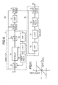
- FIG.10 a noise reduction circuit 70 shown in FIG.10, the input video signal such as the reproduced luminance signal, is applied to the input terminal 31 and is supplied to a feedback type comb filter 71.
- a feedback path of the feedback type comb filter 71 is constituted by the highpass filter 35, a limiter 72, and the coefficient multiplier 36 which are coupled in series.
- the video signal obtained from the adding circuit 34 within the feedback type comb filter 71 has a frequency characteristic in which the center frequencies of the pass bands are even number multiples of f H /2 and the center frequencies of the attenuation bands are odd number multiples of f H /2.
- the feedback type comb filter 71 is different from the feedback type comb filter 37 described before, in that the limiter 72 is provided in the feedback path of the feedback type comb filter 71.
- the comb filter characteristic of the feedback type comb filter 71 changes depending on the extent to which the vertical correlation exists in the input video signal and the amplitude of the input video signal.
- the limiter 72 has a frequency characteristic shown in FIG.11.
- the output high-frequency component of the highpass filter 35, having an amplitude between limiting levels L 1 and L 2 , is passed as it is through the limiter 72.
- the output high-frequency component of the highpass filter 35 having an amplitude which exceeds the limiting level L 1 or L 2 , is amplitude-limited to the limiting level L1 or L 2 by the limiter 72.
- the video signal which is obtained from the adding circuit 34 is the video signal component which is within the input video signal and has the vertical correlation. Hence, the high-frequency component of the output video signal of the adding circuit 34, is supplied to the limiter 72.
- the signal level at the input side of the limiter 72 will lie between the limiting levels L1 and L 2 , and the video signal applied to the limiter 72 will pass as it is and will be supplied to the coefficient multiplier 36.
- the feedback ratio of the high-frequency component becomes large in the feedback type comb filter 71, with respect to the above input video signal.
- the value of the coefficient k with respect to the high-frequency component becomes large compared to the value of the coefficient k with respect to the low-frequency component.
- the frequency characteristic of the feedback type comb filter 71 indicated by a solid line in FIG.12(A) and having an envelope characteristic la indicated by a phantom line becomes essentially the same as the frequency characteristic of the feedback type comb filter 37 described before.
- the signal level (amplitude) becomes large at the input side of the limiter 72.
- the signal level at the input side of the limiter 72 will finally exceed the limiting level L 1 or L 2 .
- the video signal applied to the limiter 72 has a large vertical correlation and a large amplitude and the signal level at the input side of the limiter 72 exceeds the limiting level L 1 or L 21 the level of the input video signal applied to the input terminal 31 becomes relatively larger than the output signal level of the coefficient multiplier 36. This means that the the feedback ratio of the feedback type comb filter 71 in the high-frequency band becomes smaller.
- an envelope characteristic Ib in the frequency characteristic of the feedback type comb filter 71 becomes as indicated by a one-dot chain line in FIG.12(A).
- the frequency characteristic of the feedback type comb filter 71 becomes essentially the same as a frequency characteristic of a comb filter having no feedback path, and an envelope characteristic Ic of the frequency characteristic in this case becomes as indicated by a phantom line in FIG.12(A). Therefore, compared to the feedback type comb filter 37 which has the same feedback ratio and no limiter, it is possible to improve the input pulse versus output pulse characteristic with respect to a video signal having an extremely large level part which is related to the vertical direction of the picture, and improve the vertical resolution of the picture.
- the output video signal of the adding circuit 34 has one of the frequency characteristics shown in FIG.12(A) depending on the level of the input video signal applied to the input terminal 31 and depending on the extent to which the vertical correlation exists in the input video signal applied to the input terminal 31.
- the output video signal is supplied to the subtracting circuit 41 and is subjected to a subtraction with the input video signal which is obtained from the input terminal 31.
- the output video signal of the adding circuit 34 is made up of the signal component which is within the input video signal (luminance signal) and has the vertical correlation.
- luminance signal luminance signal
- the output signal of the subtracting circuit 41 includes a part of the signal having the vertical correlation, because the output video signal of the adding circuit 34 has a frequency characteristic which is different from the frequency characteristic of the input video signal as may be seen from FIG.12(A).
- the output signal of the subtracting circuit 41 is supplied to a limiter 73 wherein a large amplitude part in the range of the peak-to-peak value of the noise is amplitude-limited.
- An output signal of the limiter 73 is supplied to a subtracting circuit 74.
- the subtracting circuit 74 subtracts the output signal of the limiter 73 from the input video signal which is obtained from the input terminal 31. Hence, a video signal which is reduced of the noise which appears in the vertical direction of the picture and is within the input video signal, is obtained from the subtracting circuit 74.
- the level of the signal component which is within the input video signal and has no vertical correlation is normally larger than the level of the noise.
- a circuit part which is constituted by the subtracting circuits 41 and 74 and the limiter 73, is designed to minimize the deterioration in the vertical resolution by not subtracting from the input video signal the signal component which has no vertical correlation and has a level larger than the level of the noise.
- the noise reduction circuit according to the present invention will work in principle even without this circuit part.
- the output video signal of the subtracting circuit 74 which is reduced of the noise which appears in the vertical direction of the picture, is supplied to a highpass filter 76 and to a subtracting circuit 79 within an equalizer circuit 75.
- the equalizer circuit 75 comprises the highpass filter 76, a limiter 77, a coefficient multiplier 78, and the subtracting circuit 79.
- the highpass filter 76 has a construction similar to the construction of the highpass filter 35, and has a cutoff frequency f cl2 .
- the limiter 77 and the coefficient multiplier 78 have constructions similar to the respective constructions of the limiter 72 and the coefficient multiplier 36.
- the frequency characteristic of the equalizer circuit 75 becomes as indicated by a phantom line IIa in FIG.12(B) with respect to the input video signal having a small amplitude (level) such that the signal applied to the limiter 77 will be passed through the limiter 77 as it is without being subjected to the amplitude limitation.
- the frequency characteristic of the equalizer circuit 75 is flat in the high-frequency band over the frequency fCll, flat in the low-frequency range under the frequency fcl2, and slopes at a rate of -6 d B/ oct in the frequency band between the frequencies f c11 and fcl2.
- the frequency characteristic of the equalizer circuit 75 is complementary to the envelope characteristic Ia in the frequency characteristic of the feedback type comb filter 71 shown in FIG.12(A).
- the frequency characteristic of the equalizer circuit 75 gradually changes as shown in FIG.12(B), in the sequence of the characteristics IIa, IIb, IIc, and IId.
- the frequency characteristic of the equalizer circuit 75 is variable depending on the level of the high-frequency component of the input video signal, and is complementary to the frequency characteristic of the feedback type comb filter 71 shown in FIG.12(A).
- the equalizer circuit 75 performs the operation of reducing the noise in the video signal having a small level, but also reduces the high-frequency noise regardless of the existence of the vertical correlation in the video signal.
- An output video signal of the subtracting circuit 79, is obtained through an output terminal 80.
- the frequency characteristic of the noise reduction circuit 70 shown in FIG. 10, is a sum of the frequency characteristics shown in FIGS.12(A) and 12(B).
- the frequency characteristic of the noise reduction circuit 70 assumes a comb-shaped characteristic as indicated by a solid line in FIG.12(C).
- An envelope characteristic IIIa of this frequency characteristic is a sum of the characteristics Ia and IIa shown in FIGS.12(A) and 12(B).
- the center frequencies of the pass bands are even number multiples of f H /2, and the center frequencies of the attenuation bands are odd number multiples of f H /2.
- the pass bands in the high-frequency band over the frequency f cl2 is sharper (narrower) compared to the pass bands in the low-frequency band under the frequency f c12 .
- the envelope characteristic IIIa indicated by a phantom line in FIG.12(C) which is obtained by connecting the peak levels of the pass bands, is substantially flat throughout the entire frequency band.
- the envelope characteristic in the frequency characteristic of the noise reduction circuit 70 gradually changes as shown in FIG.12(C), in the sequence of the characteristics IIIa, IIIb, and IIIc.
- the widths of the pass bands in the high-frequency band over the frequency f c12 gradually becomes wider, and finally become the same as the widths of the pass bands in the low-frequency band under the frequency fc12.
- the frequency characteristic of the noise reduction circuit 70 shown in FIG.12(C) changes depending on the level of the input video signal and the extent to which the vertical correlation exists in the input video signal.
- the center frequencies of the pass bands are always even number multiples of f H /2 and the center frequencies of the attenuation bands are always odd number multiples of f H /2.
- the frequency characteristic of the equalizer circuit 75 becomes as shown in FIG.16(B).
- the frequency characteristic of the feedback type comb filter 71 becomes as shown in FIG.16(A) which is the same as the frequency characteristic shown in FIG.12(A). 'As a result, the frequency characteristic of the noise reduction circuit 70 obtained in this case, becomes as shown in FIG.16(C).
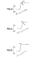
- the output signal waveform of the adding circuit 34 becomes as indicated by a solid line in FIG.13(A) when the input video signal applied to the input terminal 31 has a waveform which is in the form of a sharp pulse.
- a part of the waveform which should originally be as indicated by a phantom line a l becomes as indicated by a solid line a 2 .
- the output signal waveform of the subtracting circuit 79 becomes as indicated by a solid line in FIG.14(A).
- FIG.14(A) a part of the waveform which should originally be as indicated by a phantom line a3, becomes as indicated by a solid line a4.
- the feedback type comb filter 71 and the equalizer circuit 75 are coupled in series, and thus, the waveform shown in FIG.15(A) is obtained through the output terminal 80.
- the waveform is flat at a part a 5 , and is approximately the same as the waveform of the input video signal applied to the input terminal 31. Therefore, according to the present embodiment, it is possible to improve the input pulse versus output pulse characteristic with respect to an input video signal having the form of a pulse.
- the output signal waveform of the feedback type comb filter 71 becomes as shown in FIG.13(B).
- the waveform has parts where an overshoot occurs.
- the output signal waveform of the equalizer circuit 75 becomes as shown in FIG.14(B). Accordingly, when the staircase waveform is applied to the input terminal 31 of the noise reduction circuit 70, the waveform shown in FIG.15(B) is obtained through the output terminal 80.
- the waveform shown in FIG.15(B) is approximately the same as the waveform of the original signal which is applied to the input terminal 31.
- the feedback path of the feedback type comb filter 71 is essentially closed by the limiter 72 at least with respect to the input video signal having a large level, and the widths of the pass bands in the frequency characteristic of the feedback type comb filter 71 are widened.
- the equalizer circuit 75 has a flat frequency characteristic which is similar to a frequency characteristic obtained when there is no signal path from the highpass filter 76 to the input side of the subtracting circuit 79.
- the noise (residual noise) which cannot be reduced by a noise reduction circuit only comprising the equalizer 75, can be suppressed greatly in the high-frequency range.
- the phenomenon in which trails are formed in the horizontal direction of the picture can be made less visually conspicuous.
- the equalizer circuit 75 it is possible to couple the equalizer circuit 75 in series at the input side of the feedback type comb filter 71.
- the 1H delay circuit 33 generally comprises a charge coupled device (CCD) and a clock signal generator, and noise introduced from the clock signal generator may mix into the output signal of the lH delay circuit 33.
- the feedback type comb filter 71 introduces deterioration in the picture quality with respect to the signal component having no vertical correlation, the equalizer circuit 75 cannot compensate for this deterioration when the equalizer circuit 75 is coupled in series at the input side of the feedback type comb filter 71. Therefore, it is desirable to couple the equalizer circuit 75 as shown in the embodiment described before.
- the present invention is not limited to the embodiments described heretofore.
- a bandpass filter having a cutoff frequency which is in the range of a maximum frequency of the input video signal.
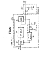
- FIG.17 shows a modification in which the output signal of the 1H delay circuit 33 is supplied to an equalizer circuit 38a.
- those parts which are the same as those corresponding parts in FIG.3 are designated by the same reference numerals, and their description will be omitted.
- the input signal voltage applied to the input terminal 31 is represented by e .
- the envelope characteristic in the frequency characteristic of the feedback type comb filter 37a is similar to the envelope characteristic I shown in FIG.4(A), but in this case, a frequency corresponding to the frequency fcll is determined by (1 - k)T and a frequency corresponding to the frequency f c12 is determined by (1 + k)T.
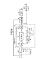
- the equalizer circuit 38 may be provided on the input side of the feedback type comb filter 37 shown in FIG.5.
- FIG.18 shows a modification in which an equalizer circuit 38b is provided on the input side of the feedback type comb filter 37.
- those parts which are the same as those corresponding parts in FIG.5 are designated by the same reference numerals, and their description will be omitted.
- the subtracting circuit 41 must be designed to perform a subtraction between the output video signal of the feedback type comb filter 37 and the input video signal applied to the input terminal 31.
- the circuit which constitutes the feedback path of the feedback type comb filter 71 comprises the highpass filter 35, the limiter 72, and the coefficient multiplier 36 which are coupled in series.
- the sequence in which the highpass filter 35, the limiter 72, and the coefficient multiplier 36 are coupled in series is not limited to the embodiment described before.
- the limiter 72 must be coupled to the output side of the highpass filter 35, however, the coefficient multiplier 36 may be coupled to the input side of the limiter 72 or to the input side of the highpass filter 35. This holds true for the highpass filter 76, the limiter 77, and the coefficient multiplier 78 of the equalizer circuit 75.
- the input video signal which is applied to the input terminal 31, is not limited to the luminance signal, and for example, color difference signals or a carrier chrominance signal may be applied to the input terminal 31.
- the carrier chrominance signal is applied to the input terminal 31, it is necessary to use an equalizer circuit having a frequency characteristic which is symmetrical about the chrominance subcarrier frequency, within a frequency range of ⁇ Af from a center frequency which is equal to the chrominance subcarrier frequency, instead of the highpass filter 35. This is because the output carrier chrominance signal will become non-symmetrical about the chrominance subcarrier frequency when the highpass filter 35 is used.
- the noise reduction circuit according to the present invention is used with respect to the carrier chrominance signal, it is necessary to use a subtracting circuit instead of the adding circuit 34.
- the present invention can be applied to the noise reduction of a luminance signal within a PAL system or SECAM system color video signal, and also to a carrier chrominance signal within the PAL system color video signal.
- the frequency of the curving point in the frequency characteristic of the equalizer circuit 75 need not coincide with that of the feedback type comb filter 71, and may be selected to other frequencies.
Landscapes
- Engineering & Computer Science (AREA)
- Multimedia (AREA)
- Signal Processing (AREA)
- Picture Signal Circuits (AREA)
- Television Signal Processing For Recording (AREA)
Applications Claiming Priority (4)
| Application Number | Priority Date | Filing Date | Title |
|---|---|---|---|
| JP223753/83 | 1983-11-28 | ||
| JP58223753A JPS60116290A (ja) | 1983-11-28 | 1983-11-28 | 映像信号の雑音低減回路 |
| JP58229348A JPS60121885A (ja) | 1983-12-05 | 1983-12-05 | 映像信号の雑音低減回路 |
| JP229348/83 | 1983-12-05 |
Publications (2)
| Publication Number | Publication Date |
|---|---|
| EP0147073A1 true EP0147073A1 (fr) | 1985-07-03 |
| EP0147073B1 EP0147073B1 (fr) | 1989-03-29 |
Family
ID=26525662
Family Applications (1)
| Application Number | Title | Priority Date | Filing Date |
|---|---|---|---|
| EP19840308247 Expired EP0147073B1 (fr) | 1983-11-28 | 1984-11-28 | Circuit de réduction du bruit pour un signal vidéo |
Country Status (2)
| Country | Link |
|---|---|
| EP (1) | EP0147073B1 (fr) |
| DE (1) | DE3477536D1 (fr) |
Cited By (3)
| Publication number | Priority date | Publication date | Assignee | Title |
|---|---|---|---|---|
| EP0175367A3 (fr) * | 1984-09-21 | 1987-03-18 | Hitachi, Ltd. | Circuit de réduction du bruit |
| EP0232597A3 (en) * | 1985-12-06 | 1989-05-31 | Matsushita Electric Industrial Co., Ltd. | Luminance signal processing circuit |
| WO2004008741A3 (fr) * | 2002-07-12 | 2004-06-24 | Snell & Wilcox Ltd | Traitement de signaux video ameliore |
Citations (2)
| Publication number | Priority date | Publication date | Assignee | Title |
|---|---|---|---|---|
| FR2437130A1 (fr) * | 1978-09-21 | 1980-04-18 | Sony Corp | Dispositif de reduction des parasites |
| US4249210A (en) * | 1978-04-03 | 1981-02-03 | British Broadcasting Corporation | Video noise reduction system |
-
1984
- 1984-11-28 DE DE8484308247T patent/DE3477536D1/de not_active Expired
- 1984-11-28 EP EP19840308247 patent/EP0147073B1/fr not_active Expired
Patent Citations (2)
| Publication number | Priority date | Publication date | Assignee | Title |
|---|---|---|---|---|
| US4249210A (en) * | 1978-04-03 | 1981-02-03 | British Broadcasting Corporation | Video noise reduction system |
| FR2437130A1 (fr) * | 1978-09-21 | 1980-04-18 | Sony Corp | Dispositif de reduction des parasites |
Non-Patent Citations (1)
| Title |
|---|
| THE BKSTS JOURNAL, vol. 60, no. 10, October 1978, pages 286,287,302, London, GB; J.O. DREWERY et al.: "An adaptive noise reducer for PAL and NTSC signals" * |
Cited By (4)
| Publication number | Priority date | Publication date | Assignee | Title |
|---|---|---|---|---|
| EP0175367A3 (fr) * | 1984-09-21 | 1987-03-18 | Hitachi, Ltd. | Circuit de réduction du bruit |
| EP0232597A3 (en) * | 1985-12-06 | 1989-05-31 | Matsushita Electric Industrial Co., Ltd. | Luminance signal processing circuit |
| WO2004008741A3 (fr) * | 2002-07-12 | 2004-06-24 | Snell & Wilcox Ltd | Traitement de signaux video ameliore |
| US7969510B2 (en) | 2002-07-12 | 2011-06-28 | Snell Limited | Video processing system and method with recursive and non-recursive filtering in separate high frequency bands |
Also Published As
| Publication number | Publication date |
|---|---|
| EP0147073B1 (fr) | 1989-03-29 |
| DE3477536D1 (en) | 1989-05-03 |
Similar Documents
| Publication | Publication Date | Title |
|---|---|---|
| US4571613A (en) | Noise reduction circuit for a video signal using a feedback type comb filter and an equalizer circuit | |
| EP0354734B1 (fr) | Amplificateur non linéaire et circuit non linéaire de préaccentuation et de désaccentuation utilisant un tel amplificateur | |
| EP0133049B1 (fr) | Appareil d'enregistrement et de reproduction de signaux vidéo | |
| US4646153A (en) | Noise reduction circuit for a video signal | |
| GB2112246A (en) | Carrier colour signal processing circuits | |
| EP0133048B1 (fr) | Système de réduction de bruit pour un signal vidéo | |
| EP0133047B1 (fr) | Dispositif d'enregistrement et de reproduction pour l'enregistrement et la reproduction d'un signal porteur de chrominance | |
| US4570193A (en) | Video signal processing device including emphasis and/or de-emphasis circuit | |
| EP0147073B1 (fr) | Circuit de réduction du bruit pour un signal vidéo | |
| EP0086496B1 (fr) | Appareil magnétique d'enregistrement et de reproduction | |
| US4348692A (en) | VTR With equalizer | |
| US5144434A (en) | Video signal processing device using look-up table | |
| EP0466442B1 (fr) | Circuits non linéaires de pré-accentuation/dé-accentuation | |
| US5276562A (en) | Emphasis apparatus disposed in either a record or playback system having triple weight coefficient generating devices | |
| JPH0810533B2 (ja) | 磁気再生装置 | |
| EP0073468A1 (fr) | Système compensateur pour manque de signal | |
| DE3201451A1 (de) | "informationswiedergabevorrichtung" | |
| EP0463885B1 (fr) | Circuit de déaccentuation non linéaire | |
| JPH0533874B2 (fr) | ||
| US5461339A (en) | Apparatus for processing frequency modulated signals | |
| DE4008937C2 (fr) | ||
| KR900003066B1 (ko) | 영상 신호의 잡음 저감회로 및 빗살형 필터 | |
| JP3139050B2 (ja) | Fm等化回路及びこれを用いた記録再生装置 | |
| JPH0575313B2 (fr) | ||
| DE3809394A1 (de) | Videogeraet mit einer entzerrerschaltung im signalweg fuer die frequenzmodulierten signale |
Legal Events
| Date | Code | Title | Description |
|---|---|---|---|
| PUAI | Public reference made under article 153(3) epc to a published international application that has entered the european phase |
Free format text: ORIGINAL CODE: 0009012 |
|
| AK | Designated contracting states |
Designated state(s): DE FR GB |
|
| EL | Fr: translation of claims filed | ||
| DET | De: translation of patent claims | ||
| 17P | Request for examination filed |
Effective date: 19851028 |
|
| 17Q | First examination report despatched |
Effective date: 19870813 |
|
| GRAA | (expected) grant |
Free format text: ORIGINAL CODE: 0009210 |
|
| AK | Designated contracting states |
Kind code of ref document: B1 Designated state(s): DE FR GB |
|
| REF | Corresponds to: |
Ref document number: 3477536 Country of ref document: DE Date of ref document: 19890503 |
|
| ET | Fr: translation filed | ||
| PLBE | No opposition filed within time limit |
Free format text: ORIGINAL CODE: 0009261 |
|
| STAA | Information on the status of an ep patent application or granted ep patent |
Free format text: STATUS: NO OPPOSITION FILED WITHIN TIME LIMIT |
|
| 26N | No opposition filed | ||
| REG | Reference to a national code |
Ref country code: GB Ref legal event code: IF02 |
|
| PGFP | Annual fee paid to national office [announced via postgrant information from national office to epo] |
Ref country code: FR Payment date: 20031110 Year of fee payment: 20 |
|
| PGFP | Annual fee paid to national office [announced via postgrant information from national office to epo] |
Ref country code: GB Payment date: 20031126 Year of fee payment: 20 |
|
| PGFP | Annual fee paid to national office [announced via postgrant information from national office to epo] |
Ref country code: DE Payment date: 20031211 Year of fee payment: 20 |
|
| PG25 | Lapsed in a contracting state [announced via postgrant information from national office to epo] |
Ref country code: GB Free format text: LAPSE BECAUSE OF EXPIRATION OF PROTECTION Effective date: 20041127 |
|
| REG | Reference to a national code |
Ref country code: GB Ref legal event code: PE20 |