EP0147810A2 - Spannungsgesteuerter Pulsoszillator mit variabler Frequenz - Google Patents
Spannungsgesteuerter Pulsoszillator mit variabler Frequenz Download PDFInfo
- Publication number
- EP0147810A2 EP0147810A2 EP84115996A EP84115996A EP0147810A2 EP 0147810 A2 EP0147810 A2 EP 0147810A2 EP 84115996 A EP84115996 A EP 84115996A EP 84115996 A EP84115996 A EP 84115996A EP 0147810 A2 EP0147810 A2 EP 0147810A2
- Authority
- EP
- European Patent Office
- Prior art keywords
- voltage
- capacitor
- gate
- controlled variable
- side gate
- Prior art date
- Legal status (The legal status is an assumption and is not a legal conclusion. Google has not performed a legal analysis and makes no representation as to the accuracy of the status listed.)
- Granted
Links
- 239000003990 capacitor Substances 0.000 claims abstract description 63
- 230000010355 oscillation Effects 0.000 claims abstract description 41
- 238000007599 discharging Methods 0.000 claims abstract description 10
- 230000003111 delayed effect Effects 0.000 claims abstract 3
- 230000007423 decrease Effects 0.000 abstract description 2
- 238000010276 construction Methods 0.000 description 12
- 238000010586 diagram Methods 0.000 description 6
- 230000005611 electricity Effects 0.000 description 2
- 238000000034 method Methods 0.000 description 2
- 230000002159 abnormal effect Effects 0.000 description 1
- 230000001934 delay Effects 0.000 description 1
- 230000000694 effects Effects 0.000 description 1
- 238000004519 manufacturing process Methods 0.000 description 1
- 238000012986 modification Methods 0.000 description 1
- 230000004048 modification Effects 0.000 description 1
- 230000002040 relaxant effect Effects 0.000 description 1
- 239000000725 suspension Substances 0.000 description 1
Images



Classifications
-
- H—ELECTRICITY
- H03—ELECTRONIC CIRCUITRY
- H03K—PULSE TECHNIQUE
- H03K3/00—Circuits for generating electric pulses; Monostable, bistable or multistable circuits
- H03K3/01—Details
- H03K3/014—Modifications of generator to ensure starting of oscillations
-
- H—ELECTRICITY
- H03—ELECTRONIC CIRCUITRY
- H03K—PULSE TECHNIQUE
- H03K3/00—Circuits for generating electric pulses; Monostable, bistable or multistable circuits
- H03K3/02—Generators characterised by the type of circuit or by the means used for producing pulses
- H03K3/023—Generators characterised by the type of circuit or by the means used for producing pulses by the use of differential amplifiers or comparators, with internal or external positive feedback
- H03K3/0231—Astable circuits
-
- H—ELECTRICITY
- H03—ELECTRONIC CIRCUITRY
- H03K—PULSE TECHNIQUE
- H03K3/00—Circuits for generating electric pulses; Monostable, bistable or multistable circuits
- H03K3/02—Generators characterised by the type of circuit or by the means used for producing pulses
- H03K3/027—Generators characterised by the type of circuit or by the means used for producing pulses by the use of logic circuits, with internal or external positive feedback
- H03K3/03—Astable circuits
-
- H—ELECTRICITY
- H03—ELECTRONIC CIRCUITRY
- H03K—PULSE TECHNIQUE
- H03K3/00—Circuits for generating electric pulses; Monostable, bistable or multistable circuits
- H03K3/02—Generators characterised by the type of circuit or by the means used for producing pulses
- H03K3/027—Generators characterised by the type of circuit or by the means used for producing pulses by the use of logic circuits, with internal or external positive feedback
- H03K3/03—Astable circuits
- H03K3/0315—Ring oscillators
- H03K3/0322—Ring oscillators with differential cells
Definitions
- the present invention relates to a voltage-controlled variable-frequency pulse oscillator, and more particularly, to a pulse oscillator which starts oscillation on its own when oscillation is interrupted due to turn on of the power supply or the like condition.
- voltage-controlled variable-frequency pulse oscillator of pulse feedback type is being utilized widely for various purposes.
- voltage of triangular wave form is generated by charging an integrating capacitors with a standard constant-current source and a voltage controllable current source, and then discharging the charged electricity through operation of a switching circuit which is connected to the capacitor.
- oscillators of the kind in which the voltage thus generated is compared with a reference voltage by a comparator, and pulse signal with prescribed frequency is outputted by means of a monostable multivibrator.
- the monostable multivibrator mentioned above is composed, for example, of an R-S flip-flop circuit obtained by connecting two OR-NOR gates in crisscross fashion.
- the OR output on the set side and the input on the reset side of the R-S flip-flop are connected via a delay circuit, and a voltage pulse is generated over the delay time of the delay circuit.
- the output terminals of the R-S flip-flop are connected to the switching circuit which is kept turned on for the duraticn of the pulse width of the voltage pulse.
- Discharge of the capacitor is carried out by the difference between the electric current of the standard constant-current source for discharge and the electric current of the current source for charging. Since the charging time of the capacitor varies according to the voltage control of the current source, the oscillator is constructed to have varying pulse frequency for the output of the R-S flip-flop in response to the controlling voltage of the voltage controllable current source.
- This oscillator includes an R-S flip-flop in which a pair of OR-NOR gates are connected in the crisscross fashion where the output Q of the gate on the set input side is fed back, via delay circuit with prescribed delay time, to the reset input of the gate on the reset side.
- this oscillator is disclosed in Japanese Patent-Publication No. 57-109416 which has already been filed by the applicant.
- the width of the pulse from the comparator has to be smaller than the discharge time of the switching circuit in order to realize an ordinary oscillation. It is noted here, for making the oscillation frequency fs large, that it is necessary to choose the discharge time of the switching circuit to be smaller than the value determined by the general condition for sustaining oscillation. As explained in the foregoing, however, the pulse width of the comparator has to be smaller than the discharge time of the switching circuit so that there is a problem that the upper limit of the oscillation frequency need be restricted.
- a pulse oscillator like the one described in the above requires an additional forced discharge circuit comprising a comparator and a switching circuit such that it was to lead to new problem like a complicated circuit construction, .large size of the oscillator itself, increased cost for manufacturing the oscillator, and so forth.
- An object of the present invention is to provide a small-sized voltage-controlled variable-frequency pulse oscillator which is capable of markedly relaxing the upper limit of the oscillation frequency as well as preventing the discontinuation of the oscillation due to turn-on of the power supply or an excessive noise current.
- Another object of the present invention is to provide a voltage-controlled variable-frequency pulse oscillator which is capable of reducing the jitter of the oscillation pulse.
- Still another object of the present invention is to provide a small-sized voltage-controlled variable-frequancy pulse oscillator capable of resuming the operation or. its own when oscillation was discontinued due to turn-on of the power supply or an excessive noise current.
- a voltage-controlled variable-frequency pulse oscillator of general type uses a reference constant current source 10 and a voltage controllable current source 12 for charging an integrating capacitor 14, and a voltage of triangular wave form is generated by discharging the charge on the capacitor 14 by the operation of a switching circuit 16 which is connected to the capacitor 14.
- the voltage thus generated is compared by a comparator 18 with the reference voltage 20 to transmit a pulse signal with prescribed frequency by means of a monostable multi-vibrator 22.
- Fig. 2 the concrete circuit construction of the monostable multivibrator 22 is illustrated. It is constructed to form an R-S flip-flop circuit by connecting a couple of OR-NOR gates 24 and 26 in the so-called crisscross fashion.
- the reset input 34 becomes [1] which causes the outputs Q 36 and Q 38 to become [1] and [0], respectively, and generates a voltage pulse for the duration of delay time of the delay circuit 32.
- the switching circuit 16 is maintained in the on state by the voltage pulse for the duration of the width of the pulse, and the discharge of the capacitor 14 is carried out by the difference between the electric current of the reference constant-current source 10 for discharge and the electric current of the current source 12 for charging.
- the . charging time of the capacitor 14 varies with the voltage control of the current source 12. Accordingly, the pulse frequency of the outputs Q 36 and Q 38 varies corresponding to the variations in the cointrolling voltage of the current source 12.
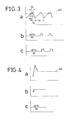
- the variaiton of the voltage between the two plates of the capacitor 14 is represented by charging and discharging over prescribed times ⁇ 1 and - ⁇ 2 , respectively, with the threshold value 40 of the comparator as the reference. This voltage is outputted from the comparator 18 in the form as shown in Fig.
- the output 36 of the R-S flip-flop circuit is given, as shown in Fig. 3C, a pulse width t d corresponding to the delay time of the delay circuit 32.
- the capacitor 14 discharges for a period of t d as shown in Fig. 3a.
- the electric current of the reference constant-current source 10 for discharge by id the capacity of the capacitor 14 by C
- shwon in Fig. 3 the discharge time of the capacitor 14 by td
- the period of the charge an discharge cycle by ts since the electricity charged in the period of t s -t d is discharged in the period of t d , as is clear from Fig. 3a, the following relation holds.
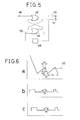
- an oscillator of the construction as shown by Fig. 1 in which the R-S flip-flop circuit is replaced by the one as shown in Fig. 5. It is equivalent to the oscillator which has been disclosed in Japanese Patent Publication No. 57-109416 filed by the present applicant. Namely, an R-S flip-flop circuit is constructed by connecting a pair of OR-NOR gates 42 and 44 in crisscross fashion, and the output Q 47 of the gate 42 on the side of the reset input 46 is fed back to the reset input 50 of the gate 44 via the delay circuit 48 with prescribed delay time.
- the time t s -t b at which the voltage of the capacitor 14 becomes less than the threshold value 40 of the comparator 18 is given by the following equation.
- t d has to remain constant as mentioned earlier and tg is the time when the voltage of the capacitor 14 exceeds the threshold 40 of the comparator until the switching circuit 16 is closed so that when fs is made large by increasing the input voltage to the current source 12, it is not possilbe, as is clear from Eq. (5), to sustain oscillation unless t d is made small. Accordingly, in a circuit construction shown in Fig. 5 which is subject to a restrictior. like Eq. (3), there exists a disadvantage that the upper limit of the oscillation frequency fs will have to be lowered to a large extent.
- a voltage-controlled variable-frequency pulse oscillator according to the present invention is provided for resolving these problems in the prior art system, and the embodiments of the invention will be described by referring to Figs. 7 to 12.
- the voltage-controlled variable-frequency pulse oscillator in accordance with the present invention includes an integrating capacitor 50, a variable current source 52 for variably setting the charging current to the capacitor 50 in response to the controlling voltage, a fixed current source 54 for discharging the capacitor 50, a switching circuit 56 for controlling the discharge, a comparator 58 for outputting a discrimination signal by comparing the voltage of the capacitor 50 and the reference voltage 57, and a monostatic multi-vibrator 60 for oscillating a pulsed signal with prescribed frequency by receiving the discrimination signal.
- the above monostatic multivibrator 60 includes an R-S flip-flop which excutes the inversion operation by inputting the discrimination signal from the comparator 58 to the set terminal, and inputting its Q output to the reset terminal via a delay circuit with prescribed delay time.
- the R-S flip flop circuit 60 includes the OR-NOR gates 64 on the set side and the OR-NOR gates 66 on the reset side, with a construction which permits to take out the output 67 of the R-S flip-flop circuit from the NOR terminal 68 of the reset-side gates 66. Furthermore, it is so constructed as to have the electric current of the fixed current source 54 to be larger than twice the maximum electric current of the variable current source 52.
- the electric current of the variable current source 52 changes with the voltage at the input 70 so that the charging current to the capacitor 50 can be varied.
- the output of the comparator 58 becomes [1] which is then inputted to the monostable multivibrator 60 comprising the OR-NOR gates 64 and 66 and a delay circuit 62.
- the switch of the differential switching circuit 56 is kept in the on state for a period of d 3 +d 2 , allowing a discharge of the capacitor 50 with constant current.
- the discharge current of the capacitor 50 is determined by the difference between the collector current of the transistor 56a and the current of the variable current source 52.
- the capacitor 50 discharges for the duration corresponding to the pulse width of the output. Then, charging starts with the [0] value of the output of Q. in this way, in the ordinary operation of the oscillator, the pulse frequency of the output can be varied by the voltage of the input 70.
- the pulse width of the output is determined by d 3 + d 2 in terms of the delay time d 3 of the delay circuit and the propagation delay d 2 of the OR-NOR gates 66 on the reset side. It should be noted that the temperature variations of the width d 3 + d 2 of the output pulse are small since the propagation delay d 2 of the OR-NOR gates is small and its temperature variations are small also. Moreover, the temperature variations of the threshold value cancel each other, and hence are small, due to the differential nature of the switch for discharge control of the capacitor 50. Therefore, the temperature variations of the time required for the comparator 50 to become [11 are small. This has an effect for suppressing the jitter of the pulse oscillator.
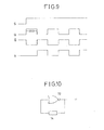
- the charging current is represented by i cmax while the discharging current is represented by ic2 - i cmax . If the charging current is chosen to satisfy i c2 - i cmax > i cemax , or i c2 > 2i cmax' the potential of the capacitor decreases gradually with ups and downs, the comparator inverts at a certain time to output [0], as shown in Fig. 11, and the self oscillation stops and an ordinary operation begins. In the figure, there is shown the output Q of the monostatic multivibrator 60 where [1] for Q represents discharge.
- the multivibrator self-oscillates and resumes the ordinary oscillation.
- the switching circuit may also be constructed ultilizing J-FETs, MOS-FETs, and the like.
- the switch for discharge control in the present embodiment has been constructed by the use of differential bipolar transistor, the operation of this section can also accomplished with a system other than the differential system.
- the monostatic multivibrator section may be constructed by the use of two NOR gates as shown in Fig. 12.
- the monostable multivibrator may be ocnstructed either by using two AND-NAND gates with inverters on the input side, as shown in Fig. 13, or by using OR-NOR gates as the set side gates and AND-NAND gates with inverters on the input side as the reset side gates, as shown in Fig. 14, or still otherwise,by using AND-NAND gates with inverters on the input side as the set side gates and OR-NOR gates as the reset side gates, as shown in Fig. 15.
- the AND-NAND gates on the set side in Fig. 13 may be replaced by AND gates
- the set side gates in Figs. 14 and 15 may be replaced by NOR gates and AND gates, respectively.
Landscapes
- Pulse Circuits (AREA)
- Inverter Devices (AREA)
- Stabilization Of Oscillater, Synchronisation, Frequency Synthesizers (AREA)
Applications Claiming Priority (2)
| Application Number | Priority Date | Filing Date | Title |
|---|---|---|---|
| JP243724/83 | 1983-12-26 | ||
| JP58243724A JPS60136412A (ja) | 1983-12-26 | 1983-12-26 | 電圧制御型可変周波数パルス発振器 |
Publications (3)
| Publication Number | Publication Date |
|---|---|
| EP0147810A2 true EP0147810A2 (de) | 1985-07-10 |
| EP0147810A3 EP0147810A3 (en) | 1985-08-07 |
| EP0147810B1 EP0147810B1 (de) | 1988-07-20 |
Family
ID=17108045
Family Applications (1)
| Application Number | Title | Priority Date | Filing Date |
|---|---|---|---|
| EP84115996A Expired EP0147810B1 (de) | 1983-12-26 | 1984-12-20 | Spannungsgesteuerter Pulsoszillator mit variabler Frequenz |
Country Status (4)
| Country | Link |
|---|---|
| US (1) | US4644300A (de) |
| EP (1) | EP0147810B1 (de) |
| JP (1) | JPS60136412A (de) |
| DE (1) | DE3472872D1 (de) |
Cited By (3)
| Publication number | Priority date | Publication date | Assignee | Title |
|---|---|---|---|---|
| EP0368398A1 (de) * | 1988-11-07 | 1990-05-16 | Koninklijke Philips Electronics N.V. | Relaxationsoszillator mit Laufzeitsteuerung und verringerter Leistungsaufnahme |
| EP0542400A1 (de) * | 1991-10-10 | 1993-05-19 | Samsung Semiconductor, Inc. | Spannungsgesteuerte Hochfrequenzoszillatorschaltung |
| EP0540661A4 (en) * | 1990-07-25 | 1993-08-11 | Power Trends, Inc | Miniaturized switching power supply having unidirectional spike filter |
Families Citing this family (18)
| Publication number | Priority date | Publication date | Assignee | Title |
|---|---|---|---|---|
| EP0675425B1 (de) * | 1989-06-30 | 1997-12-10 | Fujitsu Personal Systems, Inc. | Methode zur Reduzierung der Leistungsaufnahme eines Rechners |
| NL9201053A (nl) * | 1992-06-15 | 1994-01-03 | Koninkl Philips Electronics Nv | Switched capacitor ladingspomp, alsmede zaagtandoscillator voorzien van een dergelijke switched capacitor ladingspomp. |
| KR940011020B1 (ko) * | 1992-10-07 | 1994-11-22 | 삼성전자 주식회사 | 저주파 발진기 |
| JPH09331236A (ja) * | 1996-06-12 | 1997-12-22 | Mitsubishi Electric Corp | 電圧制御発振器および電圧制御発振器を有する非接触icカード |
| JP3567747B2 (ja) * | 1998-07-31 | 2004-09-22 | 富士通株式会社 | 電圧制御発振器及び周波数−電圧変換器 |
| KR100380158B1 (ko) * | 2000-12-29 | 2003-04-11 | 주식회사 하이닉스반도체 | 지연 회로 |
| US7145758B2 (en) * | 2002-05-17 | 2006-12-05 | International Rectifier Corporation | Arc suppression circuit for electrical contacts |
| KR101147250B1 (ko) * | 2006-01-27 | 2012-05-18 | 삼성전자주식회사 | 적응적으로 펄스 폭 변조 신호를 복조하는 복조기 및 복조방법 |
| JP5735792B2 (ja) * | 2010-12-13 | 2015-06-17 | ローム株式会社 | コンパレータ、それを利用したスイッチングレギュレータの制御回路、スイッチングレギュレータ、電子機器 |
| US8823267B2 (en) | 2011-06-10 | 2014-09-02 | Cypress Semiconductor Corporation | Bandgap ready circuit |
| US8584959B2 (en) | 2011-06-10 | 2013-11-19 | Cypress Semiconductor Corp. | Power-on sequencing for an RFID tag |
| US8665007B2 (en) | 2011-06-10 | 2014-03-04 | Cypress Semiconductor Corporation | Dynamic power clamp for RFID power control |
| US8669801B2 (en) | 2011-06-10 | 2014-03-11 | Cypress Semiconductor Corporation | Analog delay cells for the power supply of an RFID tag |
| US8729960B2 (en) | 2011-06-10 | 2014-05-20 | Cypress Semiconductor Corporation | Dynamic adjusting RFID demodulation circuit |
| US8841890B2 (en) | 2011-06-10 | 2014-09-23 | Cypress Semiconductor Corporation | Shunt regulator circuit having a split output |
| US8729874B2 (en) | 2011-06-10 | 2014-05-20 | Cypress Semiconductor Corporation | Generation of voltage supply for low power digital circuit operation |
| CN110266290B (zh) * | 2019-07-02 | 2023-02-03 | 南京中感微电子有限公司 | 一种振荡器 |
| CN111049504A (zh) * | 2019-11-22 | 2020-04-21 | 深圳市德赛微电子技术有限公司 | 一种脉冲产生电路 |
Family Cites Families (5)
| Publication number | Priority date | Publication date | Assignee | Title |
|---|---|---|---|---|
| US3364441A (en) * | 1966-03-07 | 1968-01-16 | Elastic Stop Nut Corp | Low frequency transistor relaxation oscillator |
| US3843938A (en) * | 1973-03-09 | 1974-10-22 | Us Navy | Gated clock multivibrator |
| US3924202A (en) * | 1974-08-21 | 1975-12-02 | Rca Corp | Electronic oscillator |
| JPS57109416A (en) * | 1980-12-26 | 1982-07-07 | Toshiba Corp | Voltage control variable frequency oscillator |
| US4380746A (en) * | 1981-03-03 | 1983-04-19 | Westinghouse Electric Corp. | Pulse modulator using capacitor charging and discharging circuits |
-
1983
- 1983-12-26 JP JP58243724A patent/JPS60136412A/ja active Granted
-
1984
- 1984-12-20 DE DE8484115996T patent/DE3472872D1/de not_active Expired
- 1984-12-20 EP EP84115996A patent/EP0147810B1/de not_active Expired
- 1984-12-21 US US06/685,165 patent/US4644300A/en not_active Expired - Fee Related
Cited By (3)
| Publication number | Priority date | Publication date | Assignee | Title |
|---|---|---|---|---|
| EP0368398A1 (de) * | 1988-11-07 | 1990-05-16 | Koninklijke Philips Electronics N.V. | Relaxationsoszillator mit Laufzeitsteuerung und verringerter Leistungsaufnahme |
| EP0540661A4 (en) * | 1990-07-25 | 1993-08-11 | Power Trends, Inc | Miniaturized switching power supply having unidirectional spike filter |
| EP0542400A1 (de) * | 1991-10-10 | 1993-05-19 | Samsung Semiconductor, Inc. | Spannungsgesteuerte Hochfrequenzoszillatorschaltung |
Also Published As
| Publication number | Publication date |
|---|---|
| US4644300A (en) | 1987-02-17 |
| DE3472872D1 (en) | 1988-08-25 |
| EP0147810B1 (de) | 1988-07-20 |
| JPS60136412A (ja) | 1985-07-19 |
| EP0147810A3 (en) | 1985-08-07 |
| JPH0416963B2 (de) | 1992-03-25 |
Similar Documents
| Publication | Publication Date | Title |
|---|---|---|
| EP0147810A2 (de) | Spannungsgesteuerter Pulsoszillator mit variabler Frequenz | |
| JP2531742B2 (ja) | 電圧制御発振回路 | |
| EP0613246B1 (de) | In einem grossen Bereich arbeitende veränderbare Verzögerungsleitung und Ringoszillator | |
| US4387350A (en) | Watch circuit with oscillator gain control | |
| US5565817A (en) | Ring oscillator having accelerated charging and discharging of capacitors | |
| US5532653A (en) | Supply voltage compensated charge pump oscillator | |
| JPH0799807B2 (ja) | 位相同期回路 | |
| WO2024120173A1 (zh) | Rc振荡电路 | |
| US7492231B2 (en) | Oscillator starting control circuit | |
| CN113746427B (zh) | 一种rc振荡电路 | |
| US5341113A (en) | Voltage controlled oscillator having a 50% duty cycle | |
| US4370628A (en) | Relaxation oscillator including constant current source and latch circuit | |
| CN108055021A (zh) | 振荡器 | |
| EP0328339A2 (de) | Frequenzteilerschaltung | |
| JP3087683B2 (ja) | 電圧制御発振回路 | |
| WO2007037884A2 (en) | Reducing the settling time of a crystal oscillator | |
| US6473316B2 (en) | Phase control circuit and switching regulator | |
| JPH0254698B2 (de) | ||
| US4225856A (en) | Circuit means for providing multiple audible signals from an audible tone generator means | |
| US5801566A (en) | System clock generating circuit for a semiconductor device | |
| JPH08288811A (ja) | プッシュプル駆動回路 | |
| JP3622018B2 (ja) | Dc−dcコンバータ | |
| US10601407B2 (en) | RC oscillator with comparator offset compensation | |
| US6771138B1 (en) | Method of forming a bi-directional synchronization controller | |
| JP3093140B2 (ja) | 無安定マルチバイブレータ |
Legal Events
| Date | Code | Title | Description |
|---|---|---|---|
| PUAI | Public reference made under article 153(3) epc to a published international application that has entered the european phase |
Free format text: ORIGINAL CODE: 0009012 |
|
| PUAL | Search report despatched |
Free format text: ORIGINAL CODE: 0009013 |
|
| 17P | Request for examination filed |
Effective date: 19841220 |
|
| AK | Designated contracting states |
Designated state(s): DE FR GB NL |
|
| AK | Designated contracting states |
Designated state(s): DE FR GB NL |
|
| 17Q | First examination report despatched |
Effective date: 19870127 |
|
| GRAA | (expected) grant |
Free format text: ORIGINAL CODE: 0009210 |
|
| AK | Designated contracting states |
Kind code of ref document: B1 Designated state(s): DE FR GB |
|
| REF | Corresponds to: |
Ref document number: 3472872 Country of ref document: DE Date of ref document: 19880825 |
|
| ET | Fr: translation filed | ||
| PLBE | No opposition filed within time limit |
Free format text: ORIGINAL CODE: 0009261 |
|
| STAA | Information on the status of an ep patent application or granted ep patent |
Free format text: STATUS: NO OPPOSITION FILED WITHIN TIME LIMIT |
|
| 26N | No opposition filed | ||
| PGFP | Annual fee paid to national office [announced via postgrant information from national office to epo] |
Ref country code: FR Payment date: 19981209 Year of fee payment: 15 |
|
| PGFP | Annual fee paid to national office [announced via postgrant information from national office to epo] |
Ref country code: GB Payment date: 19981224 Year of fee payment: 15 |
|
| PGFP | Annual fee paid to national office [announced via postgrant information from national office to epo] |
Ref country code: DE Payment date: 19981229 Year of fee payment: 15 |
|
| PG25 | Lapsed in a contracting state [announced via postgrant information from national office to epo] |
Ref country code: GB Free format text: LAPSE BECAUSE OF NON-PAYMENT OF DUE FEES Effective date: 19991220 |
|
| GBPC | Gb: european patent ceased through non-payment of renewal fee |
Effective date: 19991220 |
|
| PG25 | Lapsed in a contracting state [announced via postgrant information from national office to epo] |
Ref country code: FR Free format text: LAPSE BECAUSE OF NON-PAYMENT OF DUE FEES Effective date: 20000831 |
|
| PG25 | Lapsed in a contracting state [announced via postgrant information from national office to epo] |
Ref country code: DE Free format text: LAPSE BECAUSE OF NON-PAYMENT OF DUE FEES Effective date: 20001003 |
|
| REG | Reference to a national code |
Ref country code: FR Ref legal event code: ST |