EP0148157A2 - Plaquettes à circuits imprimés - Google Patents
Plaquettes à circuits imprimés Download PDFInfo
- Publication number
- EP0148157A2 EP0148157A2 EP85100063A EP85100063A EP0148157A2 EP 0148157 A2 EP0148157 A2 EP 0148157A2 EP 85100063 A EP85100063 A EP 85100063A EP 85100063 A EP85100063 A EP 85100063A EP 0148157 A2 EP0148157 A2 EP 0148157A2
- Authority
- EP
- European Patent Office
- Prior art keywords
- printed circuit
- circuit board
- thin
- mixture
- copolymer
- Prior art date
- Legal status (The legal status is an assumption and is not a legal conclusion. Google has not performed a legal analysis and makes no representation as to the accuracy of the status listed.)
- Withdrawn
Links
Images


Classifications
-
- C—CHEMISTRY; METALLURGY
- C08—ORGANIC MACROMOLECULAR COMPOUNDS; THEIR PREPARATION OR CHEMICAL WORKING-UP; COMPOSITIONS BASED THEREON
- C08L—COMPOSITIONS OF MACROMOLECULAR COMPOUNDS
- C08L23/00—Compositions of homopolymers or copolymers of unsaturated aliphatic hydrocarbons having only one carbon-to-carbon double bond; Compositions of derivatives of such polymers
- C08L23/02—Compositions of homopolymers or copolymers of unsaturated aliphatic hydrocarbons having only one carbon-to-carbon double bond; Compositions of derivatives of such polymers not modified by chemical after-treatment
- C08L23/04—Homopolymers or copolymers of ethene
- C08L23/08—Copolymers of ethene
-
- C—CHEMISTRY; METALLURGY
- C08—ORGANIC MACROMOLECULAR COMPOUNDS; THEIR PREPARATION OR CHEMICAL WORKING-UP; COMPOSITIONS BASED THEREON
- C08L—COMPOSITIONS OF MACROMOLECULAR COMPOUNDS
- C08L23/00—Compositions of homopolymers or copolymers of unsaturated aliphatic hydrocarbons having only one carbon-to-carbon double bond; Compositions of derivatives of such polymers
- C08L23/02—Compositions of homopolymers or copolymers of unsaturated aliphatic hydrocarbons having only one carbon-to-carbon double bond; Compositions of derivatives of such polymers not modified by chemical after-treatment
- C08L23/04—Homopolymers or copolymers of ethene
- C08L23/08—Copolymers of ethene
- C08L23/0846—Copolymers of ethene with unsaturated hydrocarbons containing atoms other than carbon or hydrogen
- C08L23/0853—Ethylene vinyl acetate copolymers
- C08L23/0861—Saponified copolymers, e.g. ethylene vinyl alcohol copolymers
-
- C—CHEMISTRY; METALLURGY
- C08—ORGANIC MACROMOLECULAR COMPOUNDS; THEIR PREPARATION OR CHEMICAL WORKING-UP; COMPOSITIONS BASED THEREON
- C08L—COMPOSITIONS OF MACROMOLECULAR COMPOUNDS
- C08L23/00—Compositions of homopolymers or copolymers of unsaturated aliphatic hydrocarbons having only one carbon-to-carbon double bond; Compositions of derivatives of such polymers
- C08L23/02—Compositions of homopolymers or copolymers of unsaturated aliphatic hydrocarbons having only one carbon-to-carbon double bond; Compositions of derivatives of such polymers not modified by chemical after-treatment
- C08L23/04—Homopolymers or copolymers of ethene
- C08L23/08—Copolymers of ethene
- C08L23/0846—Copolymers of ethene with unsaturated hydrocarbons containing atoms other than carbon or hydrogen
- C08L23/0869—Copolymers of ethene with unsaturated hydrocarbons containing atoms other than carbon or hydrogen with unsaturated acids, e.g. [meth]acrylic acid; with unsaturated esters, e.g. [meth]acrylic acid esters
-
- H—ELECTRICITY
- H05—ELECTRIC TECHNIQUES NOT OTHERWISE PROVIDED FOR
- H05K—PRINTED CIRCUITS; CASINGS OR CONSTRUCTIONAL DETAILS OF ELECTRIC APPARATUS; MANUFACTURE OF ASSEMBLAGES OF ELECTRICAL COMPONENTS
- H05K1/00—Printed circuits
- H05K1/02—Details
- H05K1/03—Use of materials for the substrate
- H05K1/0313—Organic insulating material
- H05K1/032—Organic insulating material consisting of one material
- H05K1/0326—Organic insulating material consisting of one material containing O
-
- H—ELECTRICITY
- H05—ELECTRIC TECHNIQUES NOT OTHERWISE PROVIDED FOR
- H05K—PRINTED CIRCUITS; CASINGS OR CONSTRUCTIONAL DETAILS OF ELECTRIC APPARATUS; MANUFACTURE OF ASSEMBLAGES OF ELECTRICAL COMPONENTS
- H05K1/00—Printed circuits
- H05K1/02—Details
- H05K1/03—Use of materials for the substrate
- H05K1/0313—Organic insulating material
- H05K1/0353—Organic insulating material consisting of two or more materials, e.g. two or more polymers, polymer + filler, + reinforcement
-
- H—ELECTRICITY
- H05—ELECTRIC TECHNIQUES NOT OTHERWISE PROVIDED FOR
- H05K—PRINTED CIRCUITS; CASINGS OR CONSTRUCTIONAL DETAILS OF ELECTRIC APPARATUS; MANUFACTURE OF ASSEMBLAGES OF ELECTRICAL COMPONENTS
- H05K1/00—Printed circuits
- H05K1/02—Details
- H05K1/03—Use of materials for the substrate
- H05K1/0313—Organic insulating material
- H05K1/0353—Organic insulating material consisting of two or more materials, e.g. two or more polymers, polymer + filler, + reinforcement
- H05K1/036—Multilayers with layers of different types
-
- H—ELECTRICITY
- H05—ELECTRIC TECHNIQUES NOT OTHERWISE PROVIDED FOR
- H05K—PRINTED CIRCUITS; CASINGS OR CONSTRUCTIONAL DETAILS OF ELECTRIC APPARATUS; MANUFACTURE OF ASSEMBLAGES OF ELECTRICAL COMPONENTS
- H05K1/00—Printed circuits
- H05K1/02—Details
- H05K1/03—Use of materials for the substrate
- H05K1/0313—Organic insulating material
- H05K1/0353—Organic insulating material consisting of two or more materials, e.g. two or more polymers, polymer + filler, + reinforcement
- H05K1/0373—Organic insulating material consisting of two or more materials, e.g. two or more polymers, polymer + filler, + reinforcement containing additives, e.g. fillers
-
- H—ELECTRICITY
- H05—ELECTRIC TECHNIQUES NOT OTHERWISE PROVIDED FOR
- H05K—PRINTED CIRCUITS; CASINGS OR CONSTRUCTIONAL DETAILS OF ELECTRIC APPARATUS; MANUFACTURE OF ASSEMBLAGES OF ELECTRICAL COMPONENTS
- H05K2201/00—Indexing scheme relating to printed circuits covered by H05K1/00
- H05K2201/09—Shape and layout
- H05K2201/09009—Substrate related
- H05K2201/09118—Moulded substrate
-
- H—ELECTRICITY
- H05—ELECTRIC TECHNIQUES NOT OTHERWISE PROVIDED FOR
- H05K—PRINTED CIRCUITS; CASINGS OR CONSTRUCTIONAL DETAILS OF ELECTRIC APPARATUS; MANUFACTURE OF ASSEMBLAGES OF ELECTRICAL COMPONENTS
- H05K3/00—Apparatus or processes for manufacturing printed circuits
- H05K3/10—Apparatus or processes for manufacturing printed circuits in which conductive material is applied to the insulating support in such a manner as to form the desired conductive pattern
- H05K3/18—Apparatus or processes for manufacturing printed circuits in which conductive material is applied to the insulating support in such a manner as to form the desired conductive pattern using precipitation techniques to apply the conductive material
- H05K3/181—Apparatus or processes for manufacturing printed circuits in which conductive material is applied to the insulating support in such a manner as to form the desired conductive pattern using precipitation techniques to apply the conductive material by electroless plating
-
- H—ELECTRICITY
- H05—ELECTRIC TECHNIQUES NOT OTHERWISE PROVIDED FOR
- H05K—PRINTED CIRCUITS; CASINGS OR CONSTRUCTIONAL DETAILS OF ELECTRIC APPARATUS; MANUFACTURE OF ASSEMBLAGES OF ELECTRICAL COMPONENTS
- H05K3/00—Apparatus or processes for manufacturing printed circuits
- H05K3/38—Improvement of the adhesion between the insulating substrate and the metal
- H05K3/388—Improvement of the adhesion between the insulating substrate and the metal by the use of a metallic or inorganic thin film adhesion layer
-
- Y—GENERAL TAGGING OF NEW TECHNOLOGICAL DEVELOPMENTS; GENERAL TAGGING OF CROSS-SECTIONAL TECHNOLOGIES SPANNING OVER SEVERAL SECTIONS OF THE IPC; TECHNICAL SUBJECTS COVERED BY FORMER USPC CROSS-REFERENCE ART COLLECTIONS [XRACs] AND DIGESTS
- Y10—TECHNICAL SUBJECTS COVERED BY FORMER USPC
- Y10S—TECHNICAL SUBJECTS COVERED BY FORMER USPC CROSS-REFERENCE ART COLLECTIONS [XRACs] AND DIGESTS
- Y10S428/00—Stock material or miscellaneous articles
- Y10S428/901—Printed circuit
-
- Y—GENERAL TAGGING OF NEW TECHNOLOGICAL DEVELOPMENTS; GENERAL TAGGING OF CROSS-SECTIONAL TECHNOLOGIES SPANNING OVER SEVERAL SECTIONS OF THE IPC; TECHNICAL SUBJECTS COVERED BY FORMER USPC CROSS-REFERENCE ART COLLECTIONS [XRACs] AND DIGESTS
- Y10—TECHNICAL SUBJECTS COVERED BY FORMER USPC
- Y10T—TECHNICAL SUBJECTS COVERED BY FORMER US CLASSIFICATION
- Y10T428/00—Stock material or miscellaneous articles
- Y10T428/24—Structurally defined web or sheet [e.g., overall dimension, etc.]
- Y10T428/24802—Discontinuous or differential coating, impregnation or bond [e.g., artwork, printing, retouched photograph, etc.]
- Y10T428/24917—Discontinuous or differential coating, impregnation or bond [e.g., artwork, printing, retouched photograph, etc.] including metal layer
-
- Y—GENERAL TAGGING OF NEW TECHNOLOGICAL DEVELOPMENTS; GENERAL TAGGING OF CROSS-SECTIONAL TECHNOLOGIES SPANNING OVER SEVERAL SECTIONS OF THE IPC; TECHNICAL SUBJECTS COVERED BY FORMER USPC CROSS-REFERENCE ART COLLECTIONS [XRACs] AND DIGESTS
- Y10—TECHNICAL SUBJECTS COVERED BY FORMER USPC
- Y10T—TECHNICAL SUBJECTS COVERED BY FORMER US CLASSIFICATION
- Y10T428/00—Stock material or miscellaneous articles
- Y10T428/31504—Composite [nonstructural laminate]
- Y10T428/31678—Of metal
- Y10T428/31692—Next to addition polymer from unsaturated monomers
Definitions
- This invention relates to printed circuit boards exhibiting excellent adhesion of a metal layer forming a circuit to a substrate at temperatures of from normal room temp$erature (about 20°C) to relatively high temperatures (e.g., 360°C) and also excellent flexibility.
- those used as three-dimensional circuit materials in equipment such as cameras, electronic calculators, telephones, printers, etc.
- a flexible copper-lined board composed of a polyimide or polyester film of about 25 ⁇ m in thickness and an electrolytic copper foil or foils of about 35 ⁇ m thickness deposited on either or both surfaces thereof and having a circuit pattern formed thereon.
- these obtained by providing this circuit pattern with through-hole plating and further providing a coaling of non-metallic substances (so called "cover-lav coating") on botn surfaces or the outer layer are also used.
- films of a polyimide or polyester resin are generally used as a base material, as described in, for example, U.S. Patents 4,377,652 and 3,322,881, Japanese Patent Publication Nos. 29793/72 and 40339/77, and Japanese Patent Application (OPI) Nos. 1123/80 and 73034/76.
- the polyester resin has a high degree of water absorption, and its coefficient of thermal expansion at 20 - 250°C is high, and thus it lacks through-hole connection reliability. Further, since curing is sometimes effected by a steam press at 170°C during production, there is a tendency, when laminated, that not only the adhesion between the resin layers, but also the flexibility thereof, are lowered.
- the polyimide film has an advantage that it can be easily soldered at an ordinary soldering temperature (260°C or higher), but has a disadvantage that since the surface activity is low, bonding with the metal foil is very difficult.
- a method is practiced of bonding using an adhesive after treating the film surface by chemical treatment using sodium hydroxide, a chromic acid mixture, aluminum hydroxide, etc.
- the board obtained generally does not have satisfactory adhesion as a printed circuit board and is poor in chemical resistance, heat resistance, etc. and thus it has various drawbacks, for example, the copper foil is loosened and comes off by etching treatment, solder flow, etc.
- thermosetting adhesive having good heat resistance e.g., an epoxy resin
- copper-lined laminates are mainly used as printed circuit boards, and demand therefor has recently been increasing.
- a phenol resin-impregnated base material and an epoxy resin-impregnated base material have been used for the copper-lined laminates.
- printed circuit boards employing base materials impregnated with these resins are not always satisfactory in various characteristics; for example, the adhesive power between the copper foil and the base material, the dimensional stability, and the electrical characteristics (especially electrical characteristics after moisture absorption treatment) are greatly lowered, and so on. Therefore, they cannot fully satisfy the demands for densification and higher reliability accompanying recent developments in the electronics fields, and thus printed circuit boards having improved capabilities are anxiously desired.
- thermoplastic resins are used as base materials
- the dimensional stability of the boards obtained is remarkably influenced by the bonding conditions using either heat fusion or the adhesive.
- residual stress of the adhesive layer acts to generate shrinkage at high temperatures, bending, twisting, etc., may be brought about.
- those having a glass cloth or mat, an inorganic fiber cloth, etc. incorporated in a base material resin are employed.
- adhesion and compatibility between the thermoplastic resin and the glass fiber are extremely poor, it is often observed that when repeatedly bent, peel-off occurs between the resin and the glass fiber, thus causing rupture, or break-down of the circuit.
- through-holes are utilized in order to connect different electrically conductive layers.
- a plated through-hole process, an additive process, a multi-wire process., etc-, axe conducted, and the through-holes are utilized also in mounting electronic parts, for example, in a clearance process, a pin inserting process, etc.
- thermosetting resin laminates generally used as printed circuit boards have not only electrical characteristics but also heat stability, and also, by making the best use of the feature of having only a small dimensional change in the thickness direction, they are used as double-faced through-hole printed circuit boards.
- thermosetting laminates that have been used include laminates obtained by impregnating a base material such as paper, cloth, glass fiber, etc., with a thermosetting resin such as a phenolic resin, an epoxy resin, an unsaturated polyester resin, etc., then drying and thereafter laminating the desired number thereof and finally heating and pressure-treating them to mold them together using a thermal press machine. Further, a disadvantage of poor heat dissipating properties is ameliorated by incorporating a good heat conductive poder filler.
- thermosetting laminates When using these thermosetting laminates as insulators for printed circuit boards, it is necessary to laminate an electrically conductive metal foil via an adhesive layer on the laminate.
- an electrically conductive metal foil As the electrically conductive metal foil, an electrolytic copper foil or a milled copper foil is used.
- finding an appropriate adhesive for bonding the copper foil and the thermosetting resin is a problem. That is, in general, an epoxy resin is used as the adhesive, but since volatile substances are contained in the adhesive, not only are blisters generated and the conductive layer comes off on heating, but also the dielectric strength is decreased, and so forth.
- the greatest disadvantages are heat resistance and moisture resistance, and since such properties in the adhesive layers are poorer than those in the thermosetting laminates, it is the present situation that the desirable characteristics of the laminates cannot be fully utilized.
- the present inventors have conducted extensive investigations in order to overcome the above-described problems and provide printed circuit boards having good heat resistance and also excellent electrical insulating properties, and, as a result, have discovered a printed circuit board having excellent electrical insulating properties as well as excellent flexibility and good durability, and thereby having accomplished this invention, viz., a printed circuit board comprising a laminate of:
- the printed board according to this invention can be composed of two layers, i.e., layer A and layer B, in order to further improve the electrical insulating properties, dimensional stability, heat resistance, chemical resistance, flexibility, and moisture resistance of the printed circuit board obtained
- layer A and layer B with a thermosetting resin layer (hereinafter referred to as "layer C"), a heat-resistant thermoplastic resin layer (hereinafter referred to as “layer D”), and a metal layer (hereinafter referred to as "layer E”), via layer A, or it is also possible to laminate layer A and layer B with layer C, layer D and layer E via the layer A and a glass cloth or mat (hereinafter referred to as "layer F").
- layer B and layer E may be laminated via .layer A, or layer A and layer F, using the layer C or the layer D as an intermediate layer.
- the printed circuit boards obtained by this invention have the following features:
- the printed circuit boards thus obtained may be subjected to bend processing and draw processing.
- the thus processed printed circuit boards have the following features:
- the printed circuit boards of this invention possess good dimensional stability, heat resistance, chemical resistance, moisture resistance, etc., as well as the electrical characteristics such as insulation resistance, dielectric constant, etc., required of the printed circuit boards of this invention, and also the folding endurance of the flexible boards exhibits flexibility which has not hitherto been obtained with the conventional boards. Further, good adhesion with the metal foil is obtained by heat contact bonding at up to relatively high temperatures (about 360°C).
- the printed circuit boards and products incorporating such obtained according to this invention manifest the above-described features, they may be used as hybrid IC (integrated circuit) boards, electrically insulating heat-conductive boards for semiconductors, boards for switching regulators, boards for chip carriers, boards for thyristors, boards for transistor arrays, etc.
- hybrid IC integrated circuit
- the crosslinked thin-wall body according to this invention is, as described hereinafter, obtained by cross- linking a thin-wall body composed of a mixture of (1) at least one of an ethylene-acrylic acid copolymer and an ethylene-methacrylic acid copolymer and (2) a saponified product of an ethylene-vinyl acetate copolymer, optionally further mixed with a heat-conductive inorganic filler, glass fiber, or a glass cloth or mat.
- the ethylene-acrylic acid copolymer and/or ethylene-methacrylic acid copolymer used in this invention may be obtained by copolymerizing ethylene and acrylic acid or ethylene and methacrylic acid at a high pressure (generally 50 kg/cm 2 or higher, and preferably 100 kg/cm 2 or higher) in the presence of a free radical generator (generally an organic peroxide).
- the copolymerization proportion of the acrylic acid or methacrylic acid in the copolymer is generally from 1 to 50% by weight, and preferably from 5 to 50% by weight. If the proportion is less than 1% by weight, a uniform thin-wall body cannot be obtained. On the other hand if it exceeds 50% by weight, the softening point is too low, and handling and transfer are inconvenient.
- the saponified product of an ethylene-vinyl acetate copolymer used in this invention is obtained by saponifying (hydrolyzing) an ethylene-vinyl acetate copolymer.
- the hydrclysis is generally conducted using sodium hydroxide in methyl alcohol.
- the ethylene-vinyl acetate copolymer starting material is obtained by copolymerizing ethylene and vinyl acetate in a manner similar to that for the aforesaid ethylene-acylic acid copolymer and ethylene-methacrylic acid copolymer.
- the copolymerization proportion of the vinyl acetate in the ethylene - vinyl acetate copolymer is generally from 1 to 60% by weight, and preferably from 5 to 50% by weight. If the proportion is less than 1% by weight, a uniform thin-wall body cannot be obtained. On the other hand, if it exceeds 60% by weight, the softening pcint is reduced, and handling at room temperature is difficult.
- the mixing proportion of copolymer (1) in the mixture according to this invention is from 20 to 80% by weight (that is, the mixing proportion of the saponified product of the ethylene-vinyl acetate copolymer is accordingly from 80 to 20% by weight), preferably from 25 to 75% by weight, and especially preferably from 30 to 70% by weight. If the mixing proportion of copolymer (1) in the mixture is less than 20% by weight, since the number of carboxyl groups (-COOH) is small as compared with the number of hydroxyl groups (-OH), the hydroxyl groups not participating in the condensation reaction would remain and thus deteriorate the heat resistance.
- such may be carried out by uniformly mixing copolymer (1) and copolymer (2).
- the mixing may be carried out, for example, by dry blending using a conventional mixer such as a Henschel mixer, or by melt kneading using a mixer such as a Banbur-y mixer, kneader, roll mill, screw type extruder, etc. It is also possible to dry blend beforehand and melt knead the resulting mixture to produce a uniform mixture.
- the carboxyl groups (-COOH) contained in copolymer (1) used in the melt kneading and the hydroxyl groups (-OH) contained in chopolymer (2) used therein undergo substantially no crosslinking reaction (condensation reaction), and no small particles of gelled product, a so-called "fish-eye", are generated in the mixture (slight cross-linking is permissible). From this point, the melting temperature is such that copolymers (1) and (2) melt, but that the cross-linking reaction does not take place (fish-eye is not generated).
- the melting temperature varies depending on whether a crosslinking accelerator as described hereinafter is present or not, and on its kind and the amount added, if no crosslinking accelerator is added, the melting temperature is generally up to 180°C, and particularly preferably from 100 to 150°C. If it is lower than 100°C, these copolymers do not completely melt, and thus a temperature lower than 100°C is not desired. On the other hand, where a crosslinking accelerator is incorporated, the melting temperature is generally from 100 to 140°C.
- the thus obtained mixture is substantially not crosslinked such that when subjected to extraction in a boiled toluene for three hours, the amount of residue (corresponding to fish-eye) is generally not more than 15% by weight, preferably not more than 10% by weight, more preferably not more than 5% by weight, based on the weight of the mixture. If it is more than 15% by weight, the mixture is difficult to torn into a thin-wall body (e.g., film and sheet) as described below.
- a thin-wall body e.g., film and sheet
- additives usually employed in the field of olefinic polymers for example, stabilizers against oxygen, light (UV) and heat, metal deterioration inhibitors, flame retardants, electrical characteristics improvers, antistatic agents, lubricants, processability improvers, tackiness improvers, etc., in amounts which do not adversely influence the characteristics of the thin-wall body of this invention.
- a crosslinking accelerator such as epoxy compounds, p-toluenesulfonic acid, aluminum-isopropoxide, etc.
- the amount thereof is generally at most 0.1 part by weight, preferably from 0.01 to 0.05 part by weight; per 100 parts by weight of these copolymers.
- a thin-wall body of this invention may be obtained by an extruder widely employed when producing films by the T-die film inflation process generally used in the field of thermoplastic resins. Further, that made into a laminate may also be used.
- the extrusion temperature is not higher than 250°C. If the extrusion is effected at a temperature higher than 250°C the copolymer (1) and copolymer (2) partially crosslink, generate fish-eye; thus a uniform extruded product cannot be obtained. Therefore, the extrusion temperature, whether a crosslinking accelerator is incorporated or not, the temperature range similar to that for the above-described melt kneading is employed.
- a thin-wall body having good transparency may be obtained.
- the thickness of the thus obtained thin-wall body is from 3 ⁇ m to less than 5 mm, and preferably from 10 ⁇ m to 1 mm taking into consideration the flexibility and the insulating properties, and particularly preferably from 10 to 400 ⁇ m.
- the thin-wall body obtained as above is substantially not crosslinked, it exhibits the same behavior as the ordinary thin-wall body.
- the thin-wall body is subjected to heating and pressure-treating at a temperature in the range of from 100 to 400°C and a pressure of at least 5 kg/cm 2 , preferably from 10 to 500 kg/cm 2 and more preferably from 15 to 200 kg/cm 2 .
- the crosslinking reaction (condensation reaction) takes place within the thin-wall body and the heat resistance is remarkably improved.
- the mixture of copolymer (1) and copolymer (2) exhibits thermoplasticity at a temperature of not higher than 250°C, but it undergoes crosslinking by heating and pressure-treating the mixture at 160°C or higher, whereby a laminate having excellent heat resistance may be obtained.
- the thin-wall body is crosslinked such that after the extraction of the crosslinked product with a boiled toluene for three hours the amount of the resulting residue having a size of 0.1 pm or more is at least 80% by weight, preferably not less than 85% by weight, more preferably 90% by weight or more, based on the weight of the crosslinked product.
- the heating and pressure-treating be carried out when laminating the uncrosslinked thin-wall body with the other constituent components (e.g., a metal foil or plate, a heat resistant polymer, a thermosetting resin, etc.), as described hereinafter.
- the other constituent components e.g., a metal foil or plate, a heat resistant polymer, a thermosetting resin, etc.
- the inorganic filler which can be incorporated in the mixture of copolymer (1) and copolymer (2) generally has a thermal conductivity of 1 x 10 -3 cal/°C ⁇ cm ⁇ sec or more and an electrical resistance value of 10 10 ⁇ cm or more, and occupied from 5 to 70% of the total volume and preferably from 20 to 60% of the total volume. If the amount filled is less than 5% of the volume, improvement in the thermal conductivity is not manifested, whereas if it exceeds 70% by volume, although the thermal conductivity is improved, the bonding ability is lowered, and thus it is not preferred.
- any inorganic filler -3 can be used which has a thermal conductivity of 1 x 10 cal/°C ⁇ cm ⁇ sec or more and an electrical resistance value of 10 10 ⁇ cm or more, representative examples thereof include beryllium oxide, boron nitride, magnesium oxide (magnesia), aluminum oxide (alumina), silicon carbide, and glass beads.
- the particle diameter of the powder of the inorganic filler is desirably not greater than 100 ⁇ m, and preferably is from 0.1 to 2 0 ⁇ m. If the particle diameter is less than 0.1 ⁇ m, it is difficult to uniformly disperse in the aforesaid mixture. On the other hand, if it exceeds 100 ⁇ m, the resulting layer A becomes too thick, and the bond strength is lowered, and thus such thickness is not desirable.
- the glass fiber which can be incorporated in the mixture of copolymer (1) and copolymer (2) generally have a fiber length of at least 0.5 mm, preferably from 1.0 to 50 mm, more preferably from 5 to 30 mm, and particularly preferably from 5 to 20 mm. If glass fibers having a fiber length of less than 0.5 mm are used, even if the amount of the glass fiber added is increased, the dimensional stability of the treated product obtained is poor, and moreover a printed circuit board having appropriate flexibility cannot be obtained. On the other hand, if a glass fiber having a fiber length of greater than 50 mm is used, it is difficult to uniformly disperse it, and thus processability is lowered. Further, a glass fiber treated with a silane compound, etc., may be preferably used.
- the proportion cf the glass fiber per 100 parts by weight of the total weight of copolymers (1) and (2) is at most 200 parts by weight, desirably from 5 to 150 parts by weight, and particularly preferably from 10 to 100 parts by weight. If the proportion of the glass is less than 5 parts by weight, the improvement in the dimensional stability is not sufficient. On the other hand, if it is incorporated in an amount of more than 200 parts by weight, the flexibility of the printed circuit board is lost, and when bent, it tends to remains bent and does not return to the original form.
- a first method is to mix copolymer (1) and copolymer (2) beforehand, and then mix glass fiber into the obtained mixture.
- a second method is to mix either copolymer (1) or copolymer (2) with glass fiber, and then mix the obtained mixture and the remaining mixing components.
- a third method is to simultaneously mix all of the mixing components.
- the glass cloth and mat which can be used in this invention include those typically employed in the glass fiber industry, i.e., roving cloth, chopped strand mat, glass cloth, etc.
- the glass cloth includes plain weave, twill weave, satin weave, designed weave, gauze weave, etc., of which the plain weave is preferred, and the density of the warp and weft is desirably from 10 to 20 lines/25 mm, preferably from 12 to 20 lines/25 mm, and more preferably from 15 to 18 lines/25 mm.$
- mats of 100 g/m 2 or less are used in 3- to 10-layered laminates, and in this invention, those obtained by laminating to a value of 300 g/m 2 or more are preferably used.
- the weight per square meter of the glass cloth or mat used in this invention is generally 300 g or more, preferably from 300 to 700 g, and particularly preferably from 350 to 700 g. If a glass cloth or mat of less than 300 g per square meter is used, flexibility of the thin-wall body obtained is lost, and hence peel-off from the conductive material, cracking, etc. are generated upon bending, and thus a weight per square meter of less than 300 g is not preferred.
- Electrically conductive metal layers that can constitute the printed circuit board of this invention are roughly classified into a metal foil and a metal layer obtained by metal plating or metal deposition.
- the thickness varies depending on whether it is either of the above-mentioned, it is generally from 100 A (10 nm) to 400 ⁇ m, preferably from 10 ⁇ m to 350 ⁇ mand particularly preferably from 15 to 350 ⁇ m.
- the electrical conductivity is generally from 10 -7 to 2 x 10 ⁇ , preferably from 10 -7 to 1 x 10 -1 ⁇ , and particularly preferably from 2 x 10 -7 to 1 x 10 -1 ⁇ .
- the thickness of the metal foil used in this invention is generally from 5 to 400 ⁇ m, preferably from 15 to 100 ⁇ m, and particularly preferably from 15 to 50 ⁇ m.
- electrically conductive metals such as copper, nickel and aluminum, and alloys mainly comprising these metals are preferred, and in particular, an electrolytic copper foil of from 15 to 40 ⁇ m in thickness is particularly preferably used.
- non-electrolytic plaing i.e., chemical plating, nickel plating, highly corrosion-resistant zinc-nickel alloy plating, copper plating, etc.
- copper sulfate plating is usually practiced, because it can provide a uniformly thick and dense plating on the entire surface contacted with the treating solution and it gives particularly excellent adherence and ductility between the material (board) and the plating.
- the crystals are minute, and leveling (uniform thickness) is imparted, and at the same time stabilized processability and excellent physical characteristics may be obtained.
- the copper sulfate plating is effected by supplying metal copper to the solution and using copper sulfate and sulfuric acid in order to enhance the electrical conductivity and uniform electrodepositing properties of the solution. Further, chlorine ions (as a catalyst) and an appropriate amount of a brightener are used. Furthermore, in order to promote leveling, a polyoxyethylene or polyoxypropylene derivative is sometimes used.
- a representative composition contains from 5 to 40 g of copper sulfate (CuSO 4 -5H 2 O) in one liter of an aqueous solution, using sodium hydroxide (NaOH), ammonium chloride (NH 4 Cl), etc., as a pH adjusting agent (buffer), disodium ethylenediaminetetraacetate (EDTA-2Na) for preventing abnormal deposition of the copper in the aqueous solution, and formaldehyde (HCHO) as a reducing agent.
- NaOH sodium hydroxide
- NH 4 Cl ammonium chloride
- EDTA-2Na disodium ethylenediaminetetraacetate
- HCHO formaldehyde
- the method of depositing a metal generally employed vacuum heating deposition such as resistance heading, electronic radiation heating, induction heating, heat radiation heating, etc., or sputtering may be used.
- the metal depositing material such metals as aluminum, gold, copper, nickel, platinum, etc., and alloys (e.g., stainless steel) mainly comprising these (50% by weight or more) may be used.
- platinum and gold are often used, and where a circuit is formed by etching after forming a thin film, copper and aluminum and an alloy mainly comprising these are preferably used.
- the thickness of the conductor thin film deposited may be freely selected depending on the conditions of the device used, it is generally from 100 A to 100 pm, and particularly desirably is from 1000 A to 20 pm.
- thermosetting resin layer and heat-resistant thermoplastic resin layer constituting the printed circuit board of this invention are those obtained from the following Thermosetting resins, polyimides polyesters, and other heat$ resistant polymers.
- the thickness thereof is generally from 0.005 to 4 mm, and particularly preferably from 0.01 to 2 mm.
- the thermosetting resin layer according to this invention may be a laminate of a thermosetting resin or a laminate impregnated with a thermosetting resin.
- a thermosetting resin a phenolic resin, an epoxy resin, and an unsaturated polyester resin may be used.
- These thermosetting resins are well known, as described in, for example, Encyclopedia of Polymer Science and Technology, Vol. 10 pp. 1-72, Vol. 6 pp. 209-270 and Vol. 11 pp. 129-168.
- the thickness of the layer is generally 0.6 to 4.0 mm, and preferably from 0.8 to 3.2 mm.
- thermosetting resin such as acrylic resin, polystyrene resin, polystyrene resin, etc., or polystyrene resin.
- these fibrous materials may be used together with pulp by making into paper by a wet paper making process similar to the ordinary paper making process.
- Representative examples include glass cloth-based epoxy resin laminates for copper Lining, etc., specifically those expressed as GE2, GE2F, GE4, and GE4F by JIS designation, paper-based phenolic resin laminates for copper lining, paper-based epoxy resin laminates for copper lining, etc.
- Polyimide film may be used as the heat-resistant thermoplastic resin layer.
- the thickness of the polyimide film used in this invention is generally from 20 ⁇ m to 2.0 mm, preferably from 50 ⁇ m to 1.6 mm, and particularly preferably from 100 ⁇ m to 1.6 mm.
- the polyimide film is generally obtained by casting a polyimide acid solution prepared by a low temperature solution polymerization process, drying and further subjecting to a dehydration ring-formation reaction.
- a polyamideimide having an amide group in the polymer backbone of the aforesaid polyimide may also be preferably employed.
- the general formula of the polyimide is shown by the following formula (I), and that of the polyamideimide by formula (II). These polymers are described in detail in Encyclopedia of Polymer Science and Technology, Vol. 11 pp. 247-272 and U.S. Patent 4,377,652. wherein n is 5 to 200.
- Polyester film may also be used as the heat-resistant thermoplastic resin layer.
- the thickness of the polyester film used in this invention is generally from 20 ⁇ m to 2.0 mm,. preferably from 50 ⁇ m to 1.6 mm, and particularly preferably from 100 ⁇ m to 1.6 mm.
- the polyester is a polymer compound containing an ester bond in the constituent molecular chain and having an aromatic ring in the chain unit of the polymer.
- This is a polymer or copolymer obtained by the condensation reaction of an aromatic dicarboxylic acid or an ester-forming derivative thereof (which may be replaced by up to 40 molar %of an aliphatic dicarboxylic acid c an alicyclic dicarboxylic acid) and an aliphatic diol having from 2 to 20 carbon atoms cr an ester-forming derivative thereof (which may be remplaced by up to 50 molar % of a long-chain glycol having a molecular weight of from 400 to 6,000).
- This pclyester has an intrinsic viscosity in the range of from 0.4 to 1.5, and preferably from 0.4 to 1.3, as measured at 30°C in a 1/1 (ratio by weight) mixed solvent of phenol and tetrachloroethane.
- Representative polyesters are polyalkylene terephthalate resins, which are widely used, such as polyethylene terephthalate, polypropylene terephthalate, and polybutylene terephthalate. These polyesters are described in Encyclopedia of Polymer Science and Technology, Vol. 11, pp. 42-120.
- polyester film Mylar by E.I. Du Pont (U.S.A.), Lumilar by Toray (Japan), Q Film by Teijin (Japan), etc., are well known.
- Heat resistant polymers having a glass transition temperature (hereinafter referred to as Tg) of from 200 to 400°C may also be used in the invention and they include those having the following polymer backbones:
- Tg glass transition temperature
- Examples of those having an amide bond as the skelton structure include: poly-m-xyleneadipoamide which is a polycondensate of xylenediamine and adipic acid poly-p-benzamide (Tg 230°C or higher) poly-p-phenylene terephthalamide (Tg 345°C) poly-m-phenylene isophthalamide (Tg 230°C or higher) etc.
- Examples of those having an ester bond as the skelton structure include polyacrylate obtained by the polycondensation of bisphenol A and isoterephthalic acid chloride , polyoxybenzoate copolymer of a condensate of p-hydroxybenzoic acid aromatic polyester carbonate which is a condensate of bisphenol
- Examples of those Having an ether bond as the skelton structure include polyoxymethylene [ CH 2 -O 1 n , polyphenylene oxide polyther sulfone . polysulfone polyether ether ketone- polyphenylene sulfide etc.
- Other examples include polytriazines (Tg 240 - 330°C), polyparabanic acid polyhydantoin, polyazomethine, polydistyryl- pyradine, etc.
- the following metal plate or foil, glass cloth and mat may be used for layer E or F.
- the metal plate used in this invention is that which may be bend and draw processed and also has a function of dissipating heat, and that having a thickness of from 0.1 to 3 mm is preferred; more preferably the thickness is from 0.1 to 2.5 mm.
- the metal material metals such as aluminum, copper, iron, etc., and alloys mainly comprising these metals (e.g., stainless steel) may be used.
- a metal plate such as an iron plate, a copper plate, etc., and also utilizing the magnetic effect, the products are apparently useful for motor magnetic circuits, communication circuit switches, electronic switching systems, heat dis- switching sipation plates, etc.
- the metal foil, glass cloth and mat used for layer E or F are the same as those described in the earlier portion of the specification, except that the thickness of the metal foil layer is generally 5 to 200 ⁇ m, preferably 5 to 100 ⁇ m and more preferably 10 to 70 ⁇ m and that the weight of the glass cloth or mat is generally not more than 2 2 2 300 g/m , preferably 50 to 250 g/m 2 and more preferably 50 to 20 0 g/m 2 .
- the thickness of the metal foil layer is generally 5 to 200 ⁇ m, preferably 5 to 100 ⁇ m and more preferably 10 to 70 ⁇ m and that the weight of the glass cloth or mat is generally not more than 2 2 2 300 g/m , preferably 50 to 250 g/m 2 and more preferably 50 to 20 0 g/m 2 .
- the process for the production of printed circuit boards by this invention may be roughly classified into the following processes if an electrically conductive metal foil or plate is used as the electrically conductive metal layer (layer B) (i.e. the production is effected without metal plating or metal deposition).
- a first process comprises inserting the thin-wall body of the substantially uncrosslinked mixture produced as described above between the aforesaid electrically conductive metal foils or plates per se or between the electrically conductive metal foil or plate and the auxiliary layer C, D, E or F (which may be used singly or as two or more layers) and subsequently heating and press-treating at a temperature and a pressure in the ranges described hereinabove.
- the auxiliary layer sometimes not used
- a second process comprises applying a process generally employed for the production of multi-layered laminates.
- the thin-wall body of the mixture obtained above is provisionally bonded uniformly to the electrically conductive metal foil with or without the auxiliary layer(s) at a temperature of 120 to 250°C and subsequently heated and pressure-treated at a temperature of 250°C or higher.
- a multi-layer formation is possible by provisionally bonding one layer upon another to laminate all the layers, and finally heating and pressure-treating the laminate.
- layer E i.e., the electrically conductive metal layer
- layer A or a laminate composed of layer A and the auxiliary layers C, D, E and F is prepared, and an electrically conductive metal is chemically plated or deposited thereon as described above.
- layer E i.e., the metal layer
- procedures similar to those described above may be conducted.
- V bending for example, generally practiced V bending, U bending, end bending, corrugation, elongation bending, etc. may be practiced, and the board laid on a die is processed using a punch. On this occasion, it is necessary to use a soft material as the punch because the punch slides on the board surface and otherwise sometimes leaves scratches.
- the so-called full additive method which involves forming a circuit by non-electrolytic copper plating or deposition on the surface or the inner surface of the through-holes of the thin-wall body may be employed or an etching step may be employed as with the copper-lined laminate.
- the insulating material used in the full additive method that coated with an adhesive on the surface is generally used, the thin-wall body obtained from copolymer (1) and copolymer (2) of this invention has excellent adhesion with non-electrolytic copper plating or deposit even without the use of an adhesive. Further, it is possible to form a conductor circuit by the convention circuit forming method.
- the mask printing agent or the photosensitive agent must have excellent alkali resistance since they are dipped in the non-electrolytic plating or the mask printing for a prolonged time.
- printed circuit beards of this invention may be subjected to any of the adhesive printing method, adhesive photographic method and direct printing method conducted by the full additive method, they are featured by that the direct printing method is also possible.
- a panel plating method which comprises making holes on a plate-formed material laminated with a copper foil, forming a copper thin film within the through-holes by non-electrolytic copper plating, then plating the entire surface by electro- lytic copper plating so as to make the hole innerwall have the predetermined copper plating thickness, then providing resist plating an organic resist corresponding to a desired circuit, and finally etching the unnecessary copper by etching;
- a pattern plating method which comprises making holes, forming a copper thin film in the through-holes by non-electrolytic copper plating or electric copper plating, then covering the part other than the pattern part with an organic resist, forming a circuit part to the predetermined copper plating thickness by electric copper plating, providing the surface with an electric plating which can stand etching, then
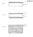
- Fig. 1 is an enlarged cross-sectional view of a part of a printed circuit board which comprises an electrically conductive metal layer 1 (corresponding to layer B) and a crosslinked thin-wall body of copolymer (1) and copolymer (2) (hereinafter referred to as an E-E resin).
- Fig. 2 is an enlarged cross-sectional view of a part of a representative example of a double-faced metal-lined printed circuit board of a structure of the printed circuit board of Fig. 1 further provided with an electrically conductive metal foil 1 on the other surface cf the cross- linked thin-wall body 2.
- Fig. 3 is an enlarged cross-sectional view cf a part of a representative example of a multi-layered printed circuit board of the structure of a laminate of single-faced and double faced metal-lined printed circuit boards as illustrated in Fig. 1, and Fig. 2.
- Fig. 4 is an enlarged cross-sectional view of a part of a representative example of a printed circuit board which comprises an electrically conductive metal layer 1 (i.e., a layer B) and an E-E resin 2 containing an inorganic filler 3.
- an electrically conductive metal layer 1 i.e., a layer B
- an E-E resin 2 containing an inorganic filler 3.
- Fig. 5 is an enlarged cross-sectional view of a part of a representative example of a printed circuit board of the structure of the printed board of Fig. 4 further provided with an electrically conductive metal foil 1 on the other surface.
- Fig. 6 is an enlarged cross-sectional view of a part of a representative example of a printed circuit board which comprises an electrically conductive metal layer 1 and an E - E resin 2 containing glass fibers 4.
- Fig. 7 is an enlarged cross-sectional view of a part of a representative example of a double-faced metal-lined printed circuit board of the structure of the printed circuit board of Fig. 6, further provided with an electrically conductive metal foil 1 on the other surface.
- Fig. 8 is an enlarged cross-sectional view of a part of a representative example of a printed circuit board which comprises an electrically conductive metal foil 1 (i.e., a layer B) and an E-E resin 2 containing glass cloth 5.
- Fig. 9 is an enlarged cross-sectional view of a part of a representative example of a double-faced metal-lined printed circuit board of the structure of the printed circuit board of F ig. 3 further provided with an electrically conductive metal foil 1 on the other surface.
- Fig. 10 is an enlarged cross-sectional view of a part of a representative example of a printed circuit board of a structure obtained by bonding an E-E resin 2 between an electrically conductive metal foil 1 and a thermosetting resin plate 6 by heating and contact bonding.
- Fig. 11 is an enlarged cross-sectional view of a part of a representative example of a double-faced metal-lined printed board of a structure of the printed circuit board of Fig. 10 further provided with a second electrically conductive metal foil 1.
- Fig. 12 is an enlarged cross-sectional view of a part of a representative example of a multi-layered of a multi-layered printed circuit board of a structure of a laminate of the single-faced and double-faced metal-lined printed circuit boards of Fig. 10 and 11.
- Fig. 13 is an enlarged cross-sectional view of a part of a representative example of a printed circuit board of a structure obtained by bonding an E-E resin 2 between an electrically conductive metal foil 1 and a heat-resistant thermoplastic resin plate 7 by heating and contact bonding.
- Fig. 14 is an enlarged cross-sectional view of a part of a representative example of a printed circuit board of a structure obtained by bonding an E-E resin 2 between an electrically conductive metal foil 1 and a metal foil or metal plate 8 by heating and contact bonding.
- Fig. 15 is an enlarged cross-sectional view of a part of a representative example of a printed circuit board obtained by bending the printed circuit board of Fig. 14.
- Fig. 16 is an enlarged cross-sectional view of a part of a representative example of a printed circuit board obtained by drawing the printed circuit board of Fig. 14.
- Fig. 17 is an enlarged cross-sectional view of a part of a representative example of a printed circuit board of a structure obtained by bonding an E-E resin 2 containing an inorganic filler 3 between an electrically conductive metal foil 1 and a thermosetting resin plate 6 bv heating and contact bondinc.
- Fig. 18 is an enlarged cross-sectional view of a part of a representative example of a printed circuit board of a structure obtained by bonding an E-E resin 2 containing a glass cloth 5 between an electrically conductive metal foil 1 and a thermosetting resin plate 6 by heating and contact bonding.
- Fig. 19 is an enlarged cross-sectional view of a part of a representative example of a modification of the printed circuit board of Fig. 17, wherein the thermosetting resin plate is replaced by a heat resistant-thermoplastic resin plate 7.
- Fig. 20 is an enlarged cross-sectional view of a part of a representative example of a modification of the printed circuit board of Fig. 18, wherein the thermosetting resin plate is replaced by a heat-resistant thermoplastic resin plate 7.
- Fig. 21 is an enlarged cross-sectional view of a part of a representative example of a modification of the printed circuit board of Fig. 17, wherein the thermosetting resin plate is replaced by a metal foil or metal plate 8.
- Fig. 22 is an enlarged cross-sectional view of a part of a representative example of a modification of the printed circuit beard of Fig. 18, wherein the thermosetting resin plate is replaced by a metal foil or metal plate 8.
- Fi g. 23 is an enlarged cross-sectional view of a part of a representative example of the double-faced copper-lined printed circuit board of Fig. 2 , particularly illustrating etching to form a circuit such as by conventional copper etching treatment.
- Fig. 24 (a), (b) and (c) are schematic cross-sectional views, illustrating steps in a procedure for forming a circuit on a double-faced through-hole board, wherein (a) shows the state wherein the parts other than that intended for the circuit formation have been masked with a masking agent 9, (b) shows the state where both surfaces have been covered with an electrically conductive metal, e.g., by non-electrolytic copper plating, deposition sputtering, etc., and (c) shows the state where the mask has been removed, whereby the circuit is formed.
- an electrically conductive metal e.g., by non-electrolytic copper plating, deposition sputtering, etc.
- the bend strength of the non-electrolytic copper by the through-hole plating is excellent, a precise pattern may be obtained as compared with conventional copper-lined boards of, e.g., glass - epoxy resin type, paper - phenolic resin type, polyimide film, polyester film, etc., and even when mass-production is conducted, produces of stabilized quality may be obtained.
- the E-E resin is flexible, no whiskers are generated and the thickness and precision of the plating may be uniformly established.
- a method for improving the hardness and the dimensional change may also be applied. These methods do not substantially lower the adherence of the non-electrolytic plating of this invention.
- the printed circuit boards obtained according to this invention not only have good heat resistance, but also have remarkably improved reliability of electrically insulating properties, and moreover have crosslinking ability and adhesion on pressure-treating at high temperatures, which have been invented based on an idea completely different from the concept in the conventional heat resistant polymer industry.
- the evaluation is expressed as follows:
- ESA ethylene-acrylic acid copolymer
- M.I. melt flow index
- Matture (B) Another mixture (hereinafter referred to as "Mixture (B)”) was prepared by procedures analogous to those above, except that the ethylene-acrylic acid copolymer used on producing the Mixture (A) was replaced by an ethylene methacrylic acid copolymer (density 0.950 g/cm 3 , methacrylic acid copolymerication proportion 25% by weight) having an M.I. of 200 g/10 min.
- Sheets of 1 mm in thickness were formed using Mixture (A), Mixture (B), EEA or the saponified product with an extruder equipped with a T-die (diameter 40 mm, die width 30 cm, rotation 85 rpm) under the temperature conditions set forth in Table 1 and taken by a water-cooled roll at 20°C.
- the obtained respective sheets were laminated with electrolytic copper foils (35 ⁇ m in thickness) using a hot press at 34°C for 10 minutes at 20 kg/cm 2 (gauge pressure) as shown in Fig. 1, and printed circuit boards were produced using the laminates, respectively.
- the properties of the obtained respective sheets and the results of the heat resistance test are set forth in Table 1.
- cross- linking degrees of the sheet (thin-wall body) before and after the lamination were measured in terms of amounts of residue having a size of 0.1 ⁇ m or more when extracted in a boiled toluene for three hours, and the results are also set forth in Table 1.
- the inorganic powders (inorganic fillers) set forth in Table 2 were mixed into the aforesaid Mixture (A), Mixture (B), EAA and the saponified product by dry blending using a Henschel mixer for 5 minutes and thereafter extruded using conditions similar to those in Example 3 to produce sheets (1.0 mm in thickness).
- the inorganic fillers used herein were boron nitride (thermal conductivity 35 Kcal/m ⁇ hr ⁇ °C, volume resistivity 10 14 ⁇ cm, hereinafter referred to as "BN") having an average particle diameter of 1.5 ⁇ m, calcium carbonate (thermal conductivity 1.0 Kcal/m ⁇ hr ⁇ °C, volume resistivity 10 14 ⁇ cm, hereinafter referred to as "CaCO 3 ”) having an average particle diameter of 5.0 ⁇ m and alumina (volume resistivity 10 16 ⁇ cm, hereinafter referred to as "Al 2 O 3 ”) having an average particle diameter of 3.0 ⁇ m.
- the resin or mixture and glass fiber set forth in Table 3 were dry blended using the amount added set forth in Table 3 in a Henschel mixer for 5 minutes.
- the obtained respective mixtures were extruded using an extruder equipped with a T-die (diameter 40 mm, die width 30 mm, rotation 85 rpm) at the same cylinder temperature and die temperature as those in Example to form sheets (500 ⁇ m in thickness).
- the thus obtained respective sheets were cross-linked by using a hot press at 340°C at 20 kg/cm 2 (gauge pressure) for 10 minutes to produce sheets.
- the obtained sheets were tested for the heat resistance. The results are given in Table 3.
- Example 12 The sheet obtained in Example 12 was measured for the volume resistivity, dielectric constant (1 MHz), dielectric loss tangent and withstand voltage according to ASTM D-257.
- the volume resistivity was 10 15 ⁇ cm, the dielectric constant was 2.9, the dielectric loss tangent was 0.02 and the withstand voltage was 25 kV/mm.
- the thin-wall body of this invention has not only excellent heat resistance but also good electrical insulating properties and thus is very useful for printed circuit boards.
- Films (200 ⁇ m in thickness) obtained analogously to that of Examples 1 to 4 and Comparative Examples 1 to 5 were overlaid with a copper foil of 35 ⁇ m in thickness on top and a glass fabric of 400 g/m 2 (hereinafter referred to as "Mat"), a cloth of 400 g/m 2 (hereinafter referred to as "Cloth (1)”) as a plain weave glass cloth or a 6-layered cloth (hereinafter referred to as "Cloth (2)”) obtained by overlaying 6 cloth to 600 g/m 2 , each being of 100 g/m 2 , on bottom, and cross-linked at 250°C or 320°C using a hot press at 20 kg/cm 2 (gauge pressure) for 10 minutes tc laminate the aforesaid film to a thickness of 1.6 mm, and thereby printed circuit boards were produced. The obtained respective boards were tested for the heat resistance under the aforesaid conditions.
- the film of 200 ⁇ m in thickness obtained in Example 22 was measured for the volume resistivity, dielectric constant (1 MHz), dielectric loss tangent and withstand voltage.
- the volume resistivity was 10 14 ⁇ cm, the dielectric constant was 3.6, the dielectric loss tangent was 0.08 and the withstand voltage was 15 HV/mm.
- Example 25 The film obtained in Example 25 was measured for the volume resistivity, dielectric constant (1 MHz), dielectric loss tangent and withstand voltage according to ASTM D-257.
- the cross-linked product (thin-wall body obtained by heating and pressure-treating the mixture) of this invention has not only good adhesion between the copper foil and the thermosetting resin base, but also excellent heat resistance and good electrical insulating properties, and therefore can be used as an adhesive for thermosetting resin-based circuit boards.
- Copper foil-laminated film obtained by laminating each film with an electrolytic copper foil (35 ⁇ m in thickness) using a laminate extruder equipped with a T-die under the conditions set forth in Table 6 was laminated with a polyimide film (trademark "Kapton” produced by du Pont, 25 ⁇ m in thickness) at 250°C or 300°C by a hot press at 20 kg/cm 2 (gauge pressure) as shown in Fig. 13, to produce each printed circuit board.
- the properties of the copper foil-laminated films obtained above are set forth in Table 6. Further, the results cf the heat resistance test of the printed circuit boards bonded (laminated) are set forth in Table 7.
- Example 33 The film obtained in Example 33 was measured for the volume resistivity, dielectric constant (1 MHz), dielectric loss tangent and withstand voltage, according to ASTM D-257.
- the volume resistivity was 10 14 ⁇ cm, the dielectric constant was 3.3, the dielectric loss tangent was 0.08, and the withstand voltage was 10 KV/mm.
- the thin-wall body cf this invention has not only excellent adhesion to the copper foil and the polyimide film but also excellent heat resistance and good electrical insulating properties, and therefore can be used as an adhesive for polyimide film-based flexible printed circuit boards.
- Films (50 ⁇ m in thickness) obtained analogously to those of Examples 1 to 4 and Comparative Examples 1 to 5 were laminated with an electrolytic copper foil (17 ⁇ m in thickness) and a polyester film (trademark "Mylar", produced by du Pont, 50 ⁇ m in thickness) at 250°C by a hot press at 20 kg/cm 2 (gauge pressure) for 10 minutes as shown in Fig. 13 to produce each printed circuit board.
- the properties of the thus obtained films are given in Table 8.
- Example 37 The film obtained in Example 37 was measured for the volume resistivity, dielectric constant (1 MHz), dielectric loss tangent and withstand voltage according to ASTM D-257.
- the volume resistivity was 10 ⁇ cm
- the dielectric constant was 3.8
- the dielectric loss tangent was 0.02
- the withstand voltage was
- the thin-wall body of this invention not only has excellent adhesion to the copper foil and the polyester film, but also excellent heat resistance and good electrical insulating properties, and therefore can be used as an adhesive for polyester film-based flexible printed circuit boards.
- Films obtained analogously to those of Examples 1 to 4 and Comparative Examples 1 to 5 were overlaid with a copper foil of 35 ⁇ m in thickness and further with a metal foil as set forth in Table 9, and cross-linked at 320°C using a hot press under a pressure of 20 kg/cm 2 (gauge pressure) for 10 minutes to produce metal foil-reinforced flexible printed circuit boards.
- a heat resistance test was conducted on each of the films obtained. The results are set forth in Table 9.
- the printed circuit boards obtained in Examples 39 to 45 could be wound round a rod of 2 cm in diameter, and no abnormality was observed even after repeating this operaticn several times. However, the printed circuit boards obtained in Comparative Examples 32 and 33 could not be wound round the aforesaid rod. Further, when the printed circuit boards obtained in Comparative. Examples 34 and 35 were wound round the aforesaid rod, peel-off was observed between the metal foil and the thin-wall body.
- Example 41 The film obtained in Example 41 was measured for the volume resistivity, dielectric constant (1 MHz), dielectric loss tangent and withstand voltage according to ASTM D-257.
- Sheets obtained analogously to those of Examples 1 to 4 and Comparative Examples 1 to 5 were provided with masking on the part other than where a circuit was to be formed using a photoresist (trademark "Ristan”, produced by du Pont) according to a photoresist masking method.
- a photoresist trademark "Ristan”, produced by du Pont
- Each sheet obtained was plated using a chemical plating solution having the following composition in one liter cf an aqueous solution at 72°C, to obtain a copper plating of about 35 ⁇ m on both surfaces of each sheet.
- each sheet was washed to remove the aforesaid masking, then washed with water, and dried.
- the printed circuit boards obtained by this invention not only have a very high circuit density, but also have excellent heat resistance and are soft, high quality printed circuit boards.
- Films obtained analogously to those of Examples 1 to 4 and Comparative Examples 1 to 5 were cross-linked at 320°C using a hot press under a pressure of 20 kg/cm 2 (gauge pressure) for 10 minutes to prepare sheets (of the thickness set forth in Table 11).
- the sheets obtained were plated using a chemical plating solution having the following composition in one liter of an aqueous solution at 72°C to obtain a copper plating of about 30 ⁇ m on both surfaces of each sheet.
- printed circuit boards obtained according to this invention not only have a very high circuit density, but also have excellent heat resistance and are soft and of a high quality.
- Platinum was deposited on the obtained sheets using a vacuum depositing device (trademark "Model JEE-4X", produced by Japan Electron Optics Lab. Co.) in 2 x 10 -6 Torr to obtain a platinum coat of about 1,000 A in thickness.
- a vacuum depositing device (trademark "Model JEE-4X", produced by Japan Electron Optics Lab. Co.) in 2 x 10 -6 Torr to obtain a platinum coat of about 1,000 A in thickness.
- the printed circuit boards obtained according to this invention not only have a very high circuit density, but also have excellent heat resistance and are soft, high-quality printed circuit boards.
- Films obtained analogously to those of Examples 1 to 4 and Comparative Examples 1 to 5 were bond laminated with electrolytic copper foils (17 ⁇ m in thickness) on both surfaces as shown in Fig. 2 and cross-linked at 320°C using a hot press under a pressure of 20 kg/cm 2 (gauge pressure) for 10 minutes to produce double-faced copper foil-lined laminates (of thicknesses as set forth in Table 13).
- Each laminate obtained was provided with through-holes of 0.5 mm of 1.0 mm in diameter and plating was effected on the through-hole part using a non-electrolytic copper plating solution having the following composition to produce each copper plating of about 20 ⁇ m in film thickness.
- a circuit was formed by firstly masking the circuit part by a screen printing machine in a conventional manner and removing the part other than the circuit by etching.
- the printed circuit boards obtained by this invention not only have a very high circuit density, but also have excellent heat resistance and are soft, high-quality printed circuit boards.
- Films obtained analogously to those of Examples 1 to 4 and Comparative Examples 1 to 5 were overlaid with an electrolytic copper foil of 35 ⁇ m in thickness on top and an aluminum plate of the thickness set forth in Table 14 on botton and cross-linked at 320°C using a hot press at 20 kg/cm 2 (gauge pressure) for 10 minutes to produce each copper-lined board for the production of hybrid integrated circuit boards.
- the boards obtained were provided with etching (amnonium persulfate etching) to give a test pattern shown in UL 796 (Printed Circuit Boards) Fig. 7.1.
- the boards obtained were subjected to a heat resistance test, a bending test by a V-die (groove width 70 mm, angle 90°, sample width 50 mm) and a square cylinder single-drawing test (no flange) (drawing depth 2 mm, corner radius 5 mm).
- the results of the heat resistance test are given in Table 14.
- the boards for printing obtained by Examples 62 to 64 did not show any disconnection of the copper circuit and were able to be processed by V-bending and drawing. Further, no peel-off was observed at the corner. On the contrary, the board obtained in Comparative Example 44 showed peel-off at the corner part on V-bending, and when drawing, the copper foil and the aluminum separated. Further, the board obtained in Comparative Example 45 showed peel-off at the corner part on V-bending, and its cut was cut on drawing.
- Films obtained analogously to those of Examples 1 to 4 and Comparative Examples 1 to 5 were laminated with an electrolytic copper foil (17 ⁇ m in thickness) and a polyether ether ketone film (50 ⁇ m in thickness) at 250°C using a hot press under a pressure of 20 kg/cm 2 (gauge pressure) for 10 minutes as shown in Fig. 13 to produce each printed board.
- the properties of the films are given in Table 15.
- Printed boards were produced in a manner similar to that in Example 65 except that the polyether ether ketone filn used in Example 65 was replaced by films of polytriazine, poly-p-phenylene phthalamide, polyoxymethylene, and polyether sulfone of 50 ⁇ m thickness, respectively.
- Example 71 The film obtained in Example 71 was measured for the volume resistivity, dielectric constant (1 MHz), dielectric loss tangent and withstand voltage according to ASTM D-257.
- the volume resistivity was 10 16 ⁇ cm, the dielectric constant was 3.8, the dielectric loss tangent was 0.02, and the withstand voltage was 10 KV/mm.
- the thin-wall bodies of this invention not only have excellent adhesion to the copper foil and the heat resistant polymer films, but also have excellent heat resistance and good electrical insulating properties, and therefore can be used as an adhesive for heat resistant polymer- based flexible printed circuit boards.
Landscapes
- Chemical & Material Sciences (AREA)
- Health & Medical Sciences (AREA)
- Chemical Kinetics & Catalysis (AREA)
- Medicinal Chemistry (AREA)
- Polymers & Plastics (AREA)
- Organic Chemistry (AREA)
- Engineering & Computer Science (AREA)
- Microelectronics & Electronic Packaging (AREA)
- Laminated Bodies (AREA)
- Insulated Metal Substrates For Printed Circuits (AREA)
Applications Claiming Priority (2)
| Application Number | Priority Date | Filing Date | Title |
|---|---|---|---|
| JP1984000029U JPS60113665U (ja) | 1984-01-05 | 1984-01-05 | 混成集積回路用基板 |
| JP29/84U | 1984-01-05 |
Publications (2)
| Publication Number | Publication Date |
|---|---|
| EP0148157A2 true EP0148157A2 (fr) | 1985-07-10 |
| EP0148157A3 EP0148157A3 (fr) | 1988-01-13 |
Family
ID=11462936
Family Applications (1)
| Application Number | Title | Priority Date | Filing Date |
|---|---|---|---|
| EP19850100063 Withdrawn EP0148157A3 (fr) | 1984-01-05 | 1985-01-03 | Plaquettes à circuits imprimés |
Country Status (3)
| Country | Link |
|---|---|
| US (1) | US4671984A (fr) |
| EP (1) | EP0148157A3 (fr) |
| JP (1) | JPS60113665U (fr) |
Cited By (6)
| Publication number | Priority date | Publication date | Assignee | Title |
|---|---|---|---|---|
| EP0206179A3 (en) * | 1985-06-15 | 1988-01-13 | Showa Denko K.K. | Molded product having printed circuit board |
| US4772496A (en) * | 1985-06-15 | 1988-09-20 | Showa Denko Kabushiki Kaisha | Molded product having printed circuit board |
| US4815981A (en) * | 1986-12-22 | 1989-03-28 | Teikoku Tsushin Kogyo Co., Ltd. | Flexible printed circuit board terminal structure |
| EP0370361A3 (fr) * | 1988-11-25 | 1991-01-09 | Bayer Ag | Mélanges polymériques, flexibles et doux d'éthylène-acétate de vinyle et de caoutchoucs acryliques |
| EP0832928A3 (fr) * | 1996-09-30 | 1998-12-09 | Kuraray Co., Ltd. | Feuille multicouche thermoformable et récipient thermoformé |
| RU2146686C1 (ru) * | 1995-09-18 | 2000-03-20 | Интернэшнл Бизнес Машинз Корпорейшн | Структура материала, содержащего поперечно-сшитый полимер биологического происхождения |
Families Citing this family (28)
| Publication number | Priority date | Publication date | Assignee | Title |
|---|---|---|---|---|
| JPH0614579B2 (ja) * | 1985-08-27 | 1994-02-23 | 三菱電線工業株式会社 | 金属芯基板及びその製造方法 |
| US5006397A (en) * | 1987-02-06 | 1991-04-09 | Key-Tech, Inc. | Printed circuit board |
| US4863757A (en) * | 1987-02-06 | 1989-09-05 | Key-Tech, Inc. | Printed circuit board |
| US4839227A (en) * | 1987-03-12 | 1989-06-13 | Minnesota Mining And Manufacturing Company | Resilient electrically and thermally conductive flexible composite |
| US4774127A (en) * | 1987-06-15 | 1988-09-27 | Tektronix, Inc. | Fabrication of a multilayer conductive pattern on a dielectric substrate |
| JP2993065B2 (ja) * | 1990-07-27 | 1999-12-20 | 三菱瓦斯化学株式会社 | 表面平滑金属箔張積層板 |
| US6124220A (en) * | 1995-03-28 | 2000-09-26 | Sumitomo Bakelite Company Limited | Laminated board and process for production thereof |
| US5928767A (en) * | 1995-06-07 | 1999-07-27 | Dexter Corporation | Conductive film composite |
| JP3579740B2 (ja) * | 1998-04-18 | 2004-10-20 | Tdk株式会社 | 電子部品の製造方法 |
| US6258203B1 (en) * | 1999-09-21 | 2001-07-10 | Ahlstrom Glassfibre Oy | Base webs for printed circuit board production using the foam process and acrylic fibers |
| US6527162B2 (en) * | 2000-08-04 | 2003-03-04 | Denso Corporation | Connecting method and connecting structure of printed circuit boards |
| US7226806B2 (en) * | 2001-02-16 | 2007-06-05 | Dai Nippon Printing Co., Ltd. | Wet etched insulator and electronic circuit component |
| JP3768908B2 (ja) * | 2001-03-27 | 2006-04-19 | キヤノン株式会社 | 電子放出素子、電子源、画像形成装置 |
| DE10145749A1 (de) * | 2001-09-17 | 2003-04-24 | Infineon Technologies Ag | Verfahren zur Herstellung einer strukturierten Metallschicht auf einem Trägerkörper und Trägerkörper mit einer strukturierten Metallschicht |
| US7258819B2 (en) * | 2001-10-11 | 2007-08-21 | Littelfuse, Inc. | Voltage variable substrate material |
| US6609915B2 (en) * | 2001-11-30 | 2003-08-26 | Fci Americas Technology | Interconnect for electrically connecting a multichip module to a circuit substrate and processes for making and using same |
| US7183891B2 (en) * | 2002-04-08 | 2007-02-27 | Littelfuse, Inc. | Direct application voltage variable material, devices employing same and methods of manufacturing such devices |
| US20070211398A1 (en) * | 2006-03-10 | 2007-09-13 | Littelfuse, Inc. | Suppressing electrostatic discharge associated with radio frequency identification tags |
| US7595112B1 (en) * | 2006-07-31 | 2009-09-29 | The United States Of America As Represented By The Administrator Of The National Aeronautics And Space Administration | Resin infusion of layered metal/composite hybrid and resulting metal/composite hybrid laminate |
| US8349143B2 (en) * | 2008-12-30 | 2013-01-08 | Intermolecular, Inc. | Shadow masks for patterned deposition on substrates |
| US8421204B2 (en) * | 2011-05-18 | 2013-04-16 | Fairchild Semiconductor Corporation | Embedded semiconductor power modules and packages |
| KR101330770B1 (ko) * | 2011-11-16 | 2013-11-18 | 엘지이노텍 주식회사 | 백라이트 유닛용 절곡 인쇄회로기판 |
| KR102070207B1 (ko) * | 2013-03-05 | 2020-01-28 | 엘지전자 주식회사 | 전도성 필름 및 이의 제조 방법, 그리고 이를 포함하는 전자 장치 |
| JP2016002669A (ja) * | 2014-06-13 | 2016-01-12 | 住友ベークライト株式会社 | 金属箔張基板、回路基板および電子部品搭載基板 |
| JP2016004841A (ja) * | 2014-06-13 | 2016-01-12 | 住友ベークライト株式会社 | 金属箔張基板、回路基板および発熱体搭載基板 |
| US10384431B2 (en) * | 2017-03-31 | 2019-08-20 | Intel Corporation | Methods for forming a substrate structure for an electrical component and an apparatus for applying pressure to an electrically insulating laminate located on a core substrate |
| US11277909B2 (en) * | 2019-08-30 | 2022-03-15 | Ttm Technologies Inc. | Three-dimensional circuit assembly with composite bonded encapsulation |
| CN111484615A (zh) * | 2020-05-11 | 2020-08-04 | 浙江中科玖源新材料有限公司 | 低热膨胀系数和吸水率的透明聚酰亚胺薄膜及制备方法 |
Family Cites Families (4)
| Publication number | Priority date | Publication date | Assignee | Title |
|---|---|---|---|---|
| DE1937548A1 (de) * | 1969-07-24 | 1971-02-11 | Licentia Gmbh | Verfahren zum Verbinden einer Metallfolie mit einem Film aus einem Homo- oder Copolymerisat des AEthylens |
| DE2411154A1 (de) * | 1974-03-08 | 1975-09-25 | Kabel Metallwerke Ghh | Basismaterial fuer gedruckte schaltungen |
| US4410612A (en) * | 1980-09-03 | 1983-10-18 | E. I. Du Pont De Nemours And Company | Electrical device formed from polymeric heat resistant photopolymerizable composition |
| US4413037A (en) * | 1981-06-17 | 1983-11-01 | Mobil Oil Corporation | Acrylic modified anionic water dispersible styrene hydroxyethyl (meth)acrylate copolymers |
-
1984
- 1984-01-05 JP JP1984000029U patent/JPS60113665U/ja active Pending
-
1985
- 1985-01-03 EP EP19850100063 patent/EP0148157A3/fr not_active Withdrawn
- 1985-01-04 US US06/688,924 patent/US4671984A/en not_active Expired - Fee Related
Cited By (7)
| Publication number | Priority date | Publication date | Assignee | Title |
|---|---|---|---|---|
| EP0206179A3 (en) * | 1985-06-15 | 1988-01-13 | Showa Denko K.K. | Molded product having printed circuit board |
| US4772496A (en) * | 1985-06-15 | 1988-09-20 | Showa Denko Kabushiki Kaisha | Molded product having printed circuit board |
| US4815981A (en) * | 1986-12-22 | 1989-03-28 | Teikoku Tsushin Kogyo Co., Ltd. | Flexible printed circuit board terminal structure |
| EP0370361A3 (fr) * | 1988-11-25 | 1991-01-09 | Bayer Ag | Mélanges polymériques, flexibles et doux d'éthylène-acétate de vinyle et de caoutchoucs acryliques |
| RU2146686C1 (ru) * | 1995-09-18 | 2000-03-20 | Интернэшнл Бизнес Машинз Корпорейшн | Структура материала, содержащего поперечно-сшитый полимер биологического происхождения |
| EP0832928A3 (fr) * | 1996-09-30 | 1998-12-09 | Kuraray Co., Ltd. | Feuille multicouche thermoformable et récipient thermoformé |
| US5972447A (en) * | 1996-09-30 | 1999-10-26 | Kuraray Co., Ltd. | Thermoformable multilayer film and thermoformed container |
Also Published As
| Publication number | Publication date |
|---|---|
| US4671984A (en) | 1987-06-09 |
| EP0148157A3 (fr) | 1988-01-13 |
| JPS60113665U (ja) | 1985-08-01 |
Similar Documents
| Publication | Publication Date | Title |
|---|---|---|
| US4671984A (en) | Printed circuit boards | |
| US4751146A (en) | Printed circuit boards | |
| US4772496A (en) | Molded product having printed circuit board | |
| CA1284089C (fr) | Stratifies electriques armes de fibres de verre, et methode de production continue pertinente | |
| CN101652401B (zh) | 环氧树脂组合物、预浸料坯、层叠板、多层印刷线路板、半导体器件、绝缘树脂片、和制造多层印刷线路板的方法 | |
| CN1131883C (zh) | 环氧树脂组合物、粘性薄膜和预浸料坯及多层印刷电路板 | |
| KR101148225B1 (ko) | 적층체의 제조 방법 | |
| EP0763562B1 (fr) | Préimpregné pour plaquettes de circuits imprimés | |
| WO2020121734A1 (fr) | Composition de résine, pré-imprégné, film fixé à une résine, feuille métallique fixée à une résine, stratifié à revêtement métallique, et carte imprimée | |
| US5674611A (en) | Adhesive for copper foils and an adhesive-applied copper foil | |
| JP7352799B2 (ja) | 樹脂組成物、プリプレグ、樹脂付きフィルム、樹脂付き金属箔、金属張積層板、及びプリント配線板 | |
| CN116376230A (zh) | 一种树脂胶液、预浸料、覆金属箔层压板与印制电路板 | |
| US4499145A (en) | Metal-clad laminate and process for producing the same | |
| TWI410187B (zh) | 用於高速及高頻印刷電路板之層壓板 | |
| JP2006124434A (ja) | エポキシ樹脂無機複合シート及び成形品 | |
| KR20220108030A (ko) | 저유전 적층체 | |
| WO2024195732A1 (fr) | Composition de résine, préimprégné, film équipé de résine, feuille métallique équipée de résine, feuille stratifiée plaquée de métal et carte de circuit imprimé | |
| EP0206179B1 (fr) | Produit moulé comportant un circuit imprimé | |
| JP2001102758A (ja) | プリント配線板とそのプリント配線板に用いる絶縁樹脂シート並びにその絶縁樹脂シートの製造方法 | |
| EP0797378A2 (fr) | Laminé revêtu de cuivre, laminé revêtu de cuivre multicouche et procédé de fabrication | |
| JPS62238742A (ja) | 耐熱性フイルム又はシ−ト | |
| JPS61110546A (ja) | フレキシブルプリント基板 | |
| JP4880841B2 (ja) | 粗化面形成用樹脂組成物を用いた多層プリント配線板 | |
| JPS62160787A (ja) | 回路基板 | |
| JPH0370917B2 (fr) |
Legal Events
| Date | Code | Title | Description |
|---|---|---|---|
| PUAI | Public reference made under article 153(3) epc to a published international application that has entered the european phase |
Free format text: ORIGINAL CODE: 0009012 |
|
| AK | Designated contracting states |
Designated state(s): BE DE FR GB IT NL |
|
| PUAL | Search report despatched |
Free format text: ORIGINAL CODE: 0009013 |
|
| AK | Designated contracting states |
Kind code of ref document: A3 Designated state(s): BE DE FR GB IT NL |
|
| 17P | Request for examination filed |
Effective date: 19880209 |
|
| 17Q | First examination report despatched |
Effective date: 19900518 |
|
| RBV | Designated contracting states (corrected) |
Designated state(s): DE FR GB NL |
|
| STAA | Information on the status of an ep patent application or granted ep patent |
Free format text: STATUS: THE APPLICATION IS DEEMED TO BE WITHDRAWN |
|
| 18D | Application deemed to be withdrawn |
Effective date: 19910103 |
|
| RIN1 | Information on inventor provided before grant (corrected) |
Inventor name: MAEDA, MASAHIKO Inventor name: SAITO, YASUTOKI Inventor name: OTANI, TAKETSUGU Inventor name: NAGATA, KAZUYASHOWA DENKO SHATAKU 235 |