EP0148396A2 - Vorrichtung zur Herstellung von einkristallinem Galliumarsenid und einkristallines Galliumarsenid hergestellt durch diese Vorrichtung - Google Patents
Vorrichtung zur Herstellung von einkristallinem Galliumarsenid und einkristallines Galliumarsenid hergestellt durch diese Vorrichtung Download PDFInfo
- Publication number
- EP0148396A2 EP0148396A2 EP84114480A EP84114480A EP0148396A2 EP 0148396 A2 EP0148396 A2 EP 0148396A2 EP 84114480 A EP84114480 A EP 84114480A EP 84114480 A EP84114480 A EP 84114480A EP 0148396 A2 EP0148396 A2 EP 0148396A2
- Authority
- EP
- European Patent Office
- Prior art keywords
- crystal
- radiation
- melt
- impurity
- single crystal
- Prior art date
- Legal status (The legal status is an assumption and is not a legal conclusion. Google has not performed a legal analysis and makes no representation as to the accuracy of the status listed.)
- Granted
Links
Images


Classifications
-
- C—CHEMISTRY; METALLURGY
- C30—CRYSTAL GROWTH
- C30B—SINGLE-CRYSTAL GROWTH; UNIDIRECTIONAL SOLIDIFICATION OF EUTECTIC MATERIAL OR UNIDIRECTIONAL DEMIXING OF EUTECTOID MATERIAL; REFINING BY ZONE-MELTING OF MATERIAL; PRODUCTION OF A HOMOGENEOUS POLYCRYSTALLINE MATERIAL WITH DEFINED STRUCTURE; SINGLE CRYSTALS OR HOMOGENEOUS POLYCRYSTALLINE MATERIAL WITH DEFINED STRUCTURE; AFTER-TREATMENT OF SINGLE CRYSTALS OR A HOMOGENEOUS POLYCRYSTALLINE MATERIAL WITH DEFINED STRUCTURE; APPARATUS THEREFOR
- C30B15/00—Single-crystal growth by pulling from a melt, e.g. Czochralski method
- C30B15/14—Heating of the melt or the crystallised materials
Definitions
- the present invention relates to an apparatus for producing a large-diameter single crystal of gallium arsenide that is doped with boron, antimony or indium as an impurity and which is substantially free of lattice defects.
- the present invention also relates to a large-diameter single crystal of gallium arsenide produced by such apparatus.
- GaAs Single-crystal gallium arsenide
- electronic devices such as field-effect transistors, light-emitting diodes and laser diodes.
- GaAs crystals are typically grown by the horizontal Bridgman method or the Czochralski method.
- HB method horizontal Bridgman method
- An advantage of the HB method is that it is capable of producing a relatively defect-free single crystal by reducing the temperature gradient.
- this method provides only an ingot of a semi-circular cross section since the growth of a single crystal occurs within the boat. When a circular wafer is sliced from the ingot by oblique cutting, a significant proportion of the crystal is wasted. Because of this materials loss, the HB method is not highly cost-effective.
- the CZ method In the Liquid Encapsulated Czochralski method (LEC method), a melt of the semiconductor is contained in a crucible and a seed crystal is dipped in the free surface of the melt. The seed is slowly pulled up out of the melt. Since the crystal growth takes place in the vertical direction, the CZ method has the advantage that a single-crystal ingot with a circular cross section can be obtained fairly easily. As a further advantage, the CZ method is sufficiently protected from the entrance of impurites to ensure the growth of a highly insulating single crystal with a high specific resistivity.
- FETs field-effect transistors
- the fabrication of field-effect transistors (FETs) requires a substrate of high specific resistivity.
- the substrate prepared by the HB method has a relatively low specific resistance since silicon atoms in the quartz boat enter the growing crystal and act as electron donors. This defect is free from the single crystals of GaAs grown by the CZ method.
- lattice defects easily occur in the single crystal grown by the CZ method since it creates a large temperature gradient at the solid-liquid interface.
- the amount of lattice defects can be estimated by counting the density of dislocations, which is equivalent to the number of etch pits in a unit area, or the etch pit density (EPD).
- EPD etch pit density
- the measurement of EPD requires the preparation of a thin wafer sliced from a grown single-crystal ingot, polishing the wafer to a mirror surface and etching the polished surface. Areas with dislocations emerge on the etched surface as small pits. The number of the small pits is counted under a microscope and is divided by the area of the wafer to obtain the etch pit density (EPD).
- etch pit density (EPD) of an ingot varies in a complex manner which can be summarized as follows:
- a single crystal of a small diameter can be easily grown by the CZ method.
- single crystals with diameters of 10 - 20 mm having EPDs in the range of 1 - 5 x 10 4 /cm 2 can be produced with relative ease.
- 2-inch (ca. 50 mm) or 3-inch (ca. 75 mm) single crystals of low EPD are difficult to prepare.
- the pinch-off voltage is an important design parameter and must be the same for all unit devices in order to assemble them into an integrated circuit. In other words, the fabrication of an integrated GaAs FET circuit is impossible without a wafer of low EPD.
- GaAs single crystals are grown by a modified Czochralski method. Having a high vapor pressure, arsenic atoms easily slip out of the melt of the compound. Even if polycrystalline GaAs is melted, its high temperature (the melting point of GaAs is 1238°C) causes the escape of arsenic in a gaseous form. The resulting deviation from stoichiometry simply produces an ingot having many As vacancies in lattices.
- the top of the melt in a crucible is covered with a melt of B 2 0 3 .
- B 2 0 3 becomes liquid, and because of its lower specific gravity than that of the molten GaAs, the latter can be completely covered with B 2 0 3 .
- the covering with B 2 O 3 is combined with filling the heating furnace with an inert gas at a pressure at least 10 atmospheres.
- B 2 O 3 provides a nearly perfect seal against the escape of As atoms from the molten GaAs.
- This technique generally referred to as the liquid encapsulated Czochralski (LEC) method, is used almost exclusively in pulling a GaAs crystal. Today, the single crystals of GaAs are seldom grown with the surface of the GaAs melt left uncovered.
- the freezing of the molten compound is desirably lowered by at least 100°C.
- the impurity must be dissolved in a large quantity in the melt.
- an impurity present in a large quantity in a single crystal provides the center for electron scattering and decreases the mobility of electrons in the crystal.
- This introduction of new lattice defects by the presence of impurities must be avoided.
- Willardson thought that good results would be obtained by using impurities which are contained in the melt in high concentrations but which do not enter the solid and are excluded from the single crystal.
- Willardson introduced the concept of "distribution coefficient".
- a substance in thermal equilibrium which has both liquid and solid phases. Add an impurity to this substance.
- the distribution of the added impurity is defined by the ratio of the amount dissolved in one unit volume of the liquid to the amount incorporated into one unit volume of the solid.
- the distribution coefficient is a phenomenalistic factor that can only be defined in the equilibrium state.
- An impurity having a distribution coefficient, k, greater than 1 is not easily dissolved in the liquid and is easily incorporated in the solid.
- An impurity with a distribution coefficient smaller than 1 is not easily incorporated in the solid and is easily dissolved in the liquid.
- Willardson et al. selected impurities that had small distribution coefficients with respect to III-V compounds.
- the present inventors evaluate this idea as a good approach.
- An impurity having a small distribution coefficient (k) can be added in a large quantity to the melt of a III-V compound, thereby lowering its freezing point (or melting point) by, for example, at least 100°C.
- this impurity will be little incorporated in the solid portion of the crystal being withdrawn upward, and the concentration of the impurity in the crystal will remain low. This would greatly alleviate the problem of lattice defects due to impurities.
- the impurity concentration would not be held constant if the single crystal is pulled by the .Czochralski method.
- the melt in the crucible is gradually exhausted.
- An impurity having a distribution coefficient, k, of less than 1 will not be incorporated in the crystal and will remain in the melt. This causes a gradual increase in the concentration of that impurity in the melt, hence in the single crystal being pulled upward. Therefore, the crystal ingot following the seed has a low impurity concentration in the top and a high impurity concentration in the bottom that is formed in the final stage of the crystal growth.
- C 0 an initial impurity concentration in the compound melt
- g a ratio of solidified part to the initial compound melt by weight and is of course smaller than unity.
- Fig. 1 reproduces the graph incorporated in Willardson's patent for showing the change in solute, or impurity, concentration with solidified fraction with parameter k varying from 0.01 to 5.
- Co is 1 for all curves.
- Willardson does not show how he derived formula (1), but his reasoning may be as follows.
- the melt in a crucible has an initial weight L a . If the solidified fraction is g, the weight of the crystal that has solidified is Log. The weight of the melt is L O (1 - g).
- the melt contains an impurity whose weight is m. In the process of single crystal growth, the melt solidifies by a small amount d (L 0 g) and this causes a decrease of the impurity content in the melt by dm.
- Distribution coefficient k is expressed as the ratio of the impurity concentration in the melt: to the impurity concentration in the solid. Since there is no movement of substances in the solid phase, only the freshly solidified portion is in equilibrium with the liquid. The weight of the freshly solidified portion is d (L 0 g) and that of the impurity incorporated in this portion is -dm. Therefore, the concentration of the impurity in the solid phase is: Since the ratio of (2) to (3) is the distribution coefficient k, we obtain the following differential equation:
- the impurity concentration C of the solid phase is plotted on the logarithmic scale as a function of the solidified fraction g. If k is smaller than 1, we obtain curves sloping upwardly and if k is greater than 1, we obtain downwardly sloping curves.
- C o is the initial impurity concentration.
- the amount of drop in the freezing point is proportional to the impurity concentration, and if the concentrations of two impurities are the same, they will cause the same amount of drop in the freezing point. Of the two impurities that have the same lowering effect of freezing point, the one that will not enter the solid phase is better.
- impurities having distribution coefficients (k) of appreciably smaller than one should be used. Therefore, Willardson postulated that impurities capable of producing III-V single crystals with minimum lattice defects should satisfy following conditions:
- the impurities the relation k ⁇ 0.02 in the AlSb crystal are B, Co, Cu, Pb, Mn and Ni.
- Cd is the only impurity that satisfies the relation k ⁇ 0.02.
- no impurity has a distribution coefficient of less than 0.02.
- the impurities that satisfy K ⁇ 0.02 in the InSb crystal are Cu, Ge, Au and Ni.
- the impurities having distribution coefficients (k) smaller than 0.02 in the GaAs crystal are Sb, Bi, Cd, Ca, Cr, Co, Cu, Fe, Pb and Ni.
- the distribution coefficient is not the only parameter that should guide the choice of an impurity; other factors must be considered such as the diffusion coefficient of the impurity, because an impurity having a large diffusion coefficient moves around in the crystal, and makes its electrical properties instable.
- copper has a distribution coefficient of less than 0.002 (a tenth of the critical level) in GaAs, and the rapid diffusion of copper will make it unsuitable for use in preparing a stoichiometric GaAs crystal. In the presence of copper, the GaAs crystal loses its electrical insulating property and becomes conductive.
- Sb, Bi, In and Pb are the elements that are advantageously added to the GaAs crystal for lowering its freezing point and reducing crystal defects.
- Whichever element is used as the impurity at least 1 x 1 0 18 atoms must be added per cm 3 of the compound.
- the crystal pulling method used by Willardson is not the LEC method but a rather unique version of the Czokralski method.
- either polycrystalline GaAs or elemental Ga and As, and an impurity are placed in a crucible and heated to form a melt.
- elementary Ga and an impurity e.g. Sb
- Arsenic is held at 605°C
- the crucible is heated to a higher temperature.
- the vapors of As enter the crucible to form a melt of GaAs.
- the seed crystal is dipped in the melt and pulled up with rotation.
- the crucible is open at the top and is not closed as in the case of the LEC method. This is in order to strike balance between the As vapor and'As in the melt.
- the temperature in the chamber must be held at 605°C except for the crucible.
- the GaAs melt forming in the crucible has acquired the liquid state at below 1238°C because the addition of an impurity such as Sb has lowered the freezing point of GaAs.
- an impurity such as Sb has lowered the freezing point of GaAs.
- Willardson says that the freezing point of GaAs is lowered by at least 100°C, so we assume GaAs may have become liquid at about 1100°C.
- Willardson's patent shows 18 examples of pulling GaAs single crystals by the modified Czochralski method using Sb, Pb and Bi as impurities.
- Half of the crystals prepared had electron mobilities in the range of 2000 - 3000 cm 2 /volt. sec. Some had values between 3000 and 4000 cm 2 /volt. sec. All crystals were doped with Te or Se to make n-type semiconductors.
- Willardson gave no example of using In as an impurity. He measured only the carrier concentrations and electron mobilities of the grown crystals. His patent says nothing about the etch pit densities of these crystals probably because he did not measure this parameter.
- Willardson et al. correlates the distribution coefficient to the freezing point lowering effect of an impurity.
- the experimental values listed in Willardson's patent are only those of electron density and its mobility. Since the electron mobility decreases as the electron density increases, a low mobility does not necessarily mean the poor characteristics of the crystal concerned. Even so, electron mobilities in the range of 2000 to 3000 cm 2 /volt. sec. are not considered very high.
- Willardson does not give experimental data for parameters other than electron density and mobility. His failure to show EPD data would be fatal to the purpose of obtaining a stoichiometrically perfect single crystal.
- the present inventors do not think that the amount of lattice defects is directly related to the electron mobility. If Willardson believes that addition of an impurity leads to fewer lattice defects, he should have measured EPD.
- Camphor which is known as a substance that is highly effective in freezing point depression has a constant for molar freezing point depression at 40°C. This means when 1000 g of camphor has 1 mol of another substance dissolved therein, the freezing point of the solution is lowered by 40°C. With water, this constant is 1.86°C and with benzene, it is 4.9°C.
- This substance contains. an impurity at a density n 2 (the number of its molecules in a unit volume).
- n 2 the number of its molecules in a unit volume.
- the ratio of the number of the molecules of the matrix to that of the molecules of the impurity is given by n l :n 2 . If the molecules of the matrix weighs 1000 g, the number of moles of the impurity is: Substituting (9) into (10), we get the number of moles of the impurity in 1000 g as follows:
- Willardson's assumption that a drop in freezing point is effective for reducing lattice defects would be based on the idea that a lower freezing point reduces the temperature gradient in both the longitudinal and radial directions of the crystal being pulled, thereby decreasing a possible thermal strain.
- a lower freezing point reduces the temperature gradient in both the longitudinal and radial directions of the crystal being pulled, thereby decreasing a possible thermal strain.
- Such effect is hardly expected from a drop in the freezing point of about 0.01°C. This is why the present inventors believe that Willardson made a mistake in evaluating the effect of a drop in freezing point.
- Willardson's method has one more defect. That is, his method is incapable of controlling the temperature in the crucible. Only the interior of the crucible is held at a high temperature Th, and the other part of the chamber is held at 605°C for maintaining the vapor pressure of arsenic constant. No arsenic is placed in the crucible as a starting material.
- the temperature in the crucible, Th is not determined by controlling a heater or other components, but by subtracting a freezing point drop ATf from the melting point of the compound, Tm: Since the impurity concentration varies in the process of pulling, ⁇ Tf changes, so does Th.
- the present inventors conclude that the invention of Willardson based on the idea of mixing a melt of GaAs with at least 10 18 atoms/cm3 of an impurity having a distribution coefficient of 0.02 or less does not achieve the intended effect, and that furthermore, his theory on the depression of freezing point is not correct.
- Mil'vidsky introduces a new concept, the critical stress of dislocation generation ⁇ c. This represents the threshold level of a stress that causes a dislocation. If a given shear stress exceeds this value, dislocation takes place, and no dislocation occurs if the stress applied is below this level.
- T c The critical stress of dislocation generation ⁇ c is high at low temperatures and low at high temperatures. At T ⁇ 0.7 Tm, the value of T c is extremely small.
- Mil'vidsky's theory The most important thing about Mil'vidsky's theory is that the doping to a crystal with an impurity causes an increase in the critical shear stress ⁇ c. Mil'vidsky explains the mechanism of increased T c due to doping as follows. He starts with the concept of "movement of a dislocation". Dislocation can be considered as an entity that moves by itself. After one dislocation has moved, another dislocation is formed. A shear force causes rapid movement of dislocations, or high multiplication of dislocations. However, an impurity blocks the movement of dislocations, hence their multiplication.
- the force of blocking the movement of a dislocation is proportional to the square of the difference between the volume of the matrix element Vo and the volume of an impurity V l , and is in inverse proportion to the diffusion coefficient D of the impurity atom.
- the blocking force is proportional to the value of Q which is given by:
- Mil'vidsky gives experimental data that shows the decrease in EPD by increasing the concentrations of dopants (Te, In, Sn and Zn) in GaAs single crystals grown by the LEC method. This data is shown graphically as Fig. 4 in Mil'vidsky's paper and is attached to this specification as Fig. 2, wherein the impurity concentration is plotted on the x-axis and Nd (or EPD in cm -2 ) on the y-axis.
- the grown single crystals were 20 - 25 mm in diameter. With Te doping in concentrations between 5 x 10 18 and 1 x 10 19 cm -3 , Nd was less than 10/cm .
- the In concentration can be expressed in terms of ni as follows:
- the effect of the difference between the volumes of the matrix and impurity elements is that of second degree.
- the radius of a gallium atom is smaller than that of an indium atom and greater than that of an aluminum atom. If either impurity is doped at the Ga site, the volume effect will be the same for each impurity since the effect is of second degree.
- a dislocation in a crystal can be regarded as a line growing in the axial direction. Mil'vidsky postulates that the dislocation stops moving if the line of dislocation collides against an impurity atom. However, it is strange that impurity atoms having a cross section of collision of 10-6 can block dislocations of a density of 10 5 /cm 2 and reduce their density to 100 - 1000/cm 2 .
- Q in Eq. (15) is obtained by dividing the square of volume difference by diffusion coefficient D. This would be a kind of makeshift that has been managed to differentiate the volume effects of two impurity elements which do not make a great difference as far as the square of the volume difference from the matrix element is concerned.
- tellurium which, according to Mil'vidsky, is the most effective dopant in diminishing the dislocation density in GaAs.
- the ionic radius of As 3- is 2.22 whereas Te 2- has an ionic radius of 2.21 A (see Tables of Physical Constants, New. Ed., published by Asakura Shoten, 1978, p. 211).
- the Tables also show that Ga 3+ and Sn 4+ respectively have ionic radii of 0.62 A and 0.69 A.
- the volume of an As atom little changes even if its site is replaced by Te, so does the volume of a Ga atom replaced by Sn.
- the square of the difference in volume between As and Te or between Ga and Sn is almost zero.
- a single crystal is cylindrical; when it is pulled upward from the melt its peripheral portion is first cooled by heat dissipation. The center of the crystal is still hot. The cooling peripheral portion contracts and a stress develops in the crystal.
- the present inventors postulate that the generation of dislocation is related more closely to the primary stress ⁇ 1 than to the shear force.
- the effect of the principal stress ⁇ 1 on the amount of EPD will vary between tensile stress ( ⁇ 1 >0) and compressive stress ( ⁇ 1 ⁇ 0). Shear force would also contribute to the generation of dislocations.
- Dislocation induction coefficient This factor includes tension coefficient 6, compression coefficient ⁇ and shear coefficient y.
- Dislocation induction coefficient is defined as the number of EPDs induced per unit quantity that is the square of stress. Since compressive stress occurs when r ⁇ r 2 and tensile stress when r>r 2 , the EPD hypothesis of the present inventors can be expressed by the following formulas ( ⁇ is written for yl):
- Fig. 4 Data supporting the above conclusion are shown in Fig. 4. They show the EPD distributions in ⁇ 100> and ⁇ 110> directions of an etched wafer sliced from an undoped GaAs single crystal that was grown by a JUMBO furnace of Cambridge Instrument Company, Inc. England.
- the EPD is plotted on the y-axis and ranges from 5 m 16 x 10 4 /cm 2 .
- the EP D is the highest in the center and on the periphery and assumes values of about 15 x 10 4 /cm 2 .
- Minimum EPD in the ⁇ 110> direction is about 5 x 10 4 /cm 2 and minimum EPD in the ⁇ 100> direction is about 7 x 10 4 /cm 2.
- EPD values in the ⁇ 100> direction are greater than those in the ⁇ 110> direction because, as already mentioned, the direction of shear force ⁇ coincides with the cleavage direction.
- y is greater in the ⁇ 100> direction than in the ⁇ 110> direction.
- y is expressed by wherein y0 and e are constants.
- Equations (51) and (52) the present inventors postulate as formulas that explain the EPD distribution across a single-crystal GaAs are graphed in Fig. 5. As shown, the distribution is a W-shaped function:
- Normalized stress a O is given by Eq. (41'), but this equation does not show the exact power of radius (R) as the proportionality constant for normalized stress.
- Eq. (28) we obtain 2aR as the temperature gradient in the radial direction of the crystal surface. Multiplying this by thermal conductivity, we obtain heat dissipation from a unit area by radiation and convection.
- the heat dissipation defined as above should be constant irrespective of the crystal diameter if the furnace construction, heater temperature and the height of the crystal from the melt surface are the same. In other words, the product of temperature gradient coefficient a and radius R is constant. Therefore, normalized stress ⁇ 0 is proportional to the first power of R.
- EPD defined by Eq.
- the present inventors postulate that the effect of an impurity is reflected in thermal expansion coefficient in Eq. (41').
- the temperature of a single crystal being pulled upward decreases from the peripheral portion toward the center.
- the resulting isotherm is convex upward.
- a heat flow occurs in a direction perpendicular to the isotherm and is directed from the center bottom toward the top at an angle with respect to the longitudinal axis.
- the periphery of the crystal is cooled and begins to contract.
- the contracting area (r 3 ⁇ r) is subject to tensile stress.
- Tensile stress is significantly relaxed by substitution of an element which is larger in size than matrix elements such as Ga and As. Relaxation of tensile stress means an effective decrease in expansion coefficient a. Larger impurity elements were already present in the liquid state, so one may wonder why they are capable of relaxing the tensile stress in a solidified crystal.
- a liquid substance has only a short-distance order over atoms. The incorporation of an impurity causes a volume increase corresponding to only one atom. The arrangement of atoms in a solid has a long-distance order.
- an impurity of a large size replaces Ga or As, not only does a volume increase occur corresponding to the impurity atom but also the lattice distance between neighboring Ga and As is increased because this requires a lower energy.
- an impurity of a large size causes a volume increase.
- the lattice distance between matrix elements Ga and As becomes shorter.
- the two competing forces are balanced and expansion coefficient a, hence ⁇ 0 , effectively approaches zero.
- more impurity atoms are incorporated in the crystal lattice in an area of a larger radius than in an area having a smaller radius.
- the center of the crystal being pulled is also solidified and contracts in size.
- the contracting force originates from the tensile force acting in the peripheral portion. A decrease in the tensile force causes a corresponding decrease in the contracting force. Under the contracting force, atoms of the large-size impurity move downward and come toward the central portion of the crystal. The remaining impurity atoms are left in the center. This causes a high EPD in the center of the crystal.
- expansion coefficient a is very small, the volume increase due to the impurity present in an amount of a few percent or less is sufficient to substantially cancel the contraction of the crystal due to cooling.
- R In order to decrease ⁇ 0' R may be reduced, but R must be large enough to meet . economical and industrial requirements. The only choice will then be by reducing a, or the coefficient providing a thermal gradient. As Eq. (41') shows, a decrease in a leads to a smaller ⁇ 0 . One may well state that a decrease in a permits a greater R.
- the impurity is effective in bringing expansion coefficient a to its initial value (when GaAs is undoped). Since, according to Eq. (41'), ⁇ need not be appreciably small if a is small, the doping level of the impurity can be decreased if the temperature distribution is highly uniform.
- the primary object of the present invention is to provide an apparatus for preparing a GaAs single crystal which is substantially free of lattice defects.
- Another object of the invention is to provide a nearly perfect GaAs single crystal prepared by this apparatus.
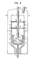
- Fig. 6 is a sectional view of the pulling apparatus of the present invention for growing a GaAs single crystal.
- the apparatus is basically a Czochralski furnace but differs from the conventional type in that it includes two or more heaters and the top of the furnace is covered with a double radiation/ convection shielding mechanism.
- An upper heater indicated at 1 is cylindrical and is primarily used to heat the crystal pulled above the melt surface so as to prevent a rapid drop in the crystal temperature.
- a lower heater 2 is also cylindrical in the principal part and its primary function is to heat that part of a crucible which is filled with the compound (GaAs) melt. The lower heater 2 is positioned just below the upper heater 1.
- Both upper heater 1 and lower heater 2 are shaped from carbon resistance material.
- a carbon tube is provided with vertical grooves in which current flows alternately in upward and downward directions.
- Both ends of each heater extend downwardly to be connected to electrodes (not shown).
- Susceptor 3 and crucible 4 are disposed in a vertically slidable and rotatable manner in the center of the space surrounded by heaters 1 and 2.
- Susceptor 3 is typically made of carbon and crucible 4 is typically made of pyrolytic boron nitride (PBN).
- PBN pyrolytic boron nitride
- a quartz crucible should not be used because Si escapes into the compound melt to form an n-type semiconductor.
- the product that is to be prepared by the apparatus of the present invention is a semi-insulating semiconductor with a minimum carrier concentration. In order to prevent the entrance of Si, the use of a quartz crucible should be avoided.
- Upper heater 1 is provided on its top with a first radiation/convection shielding tube 16 which is tubular and whose upper portion has a circular cross section.
- the lower end of the first radiation/convection shielding tube 16 is positioned close to the upper end of the heater 1.
- the gap g between the lower end of the first shielding tube 16 and the upper end of the heater 1 is made sufficiently small to minimize the occurrence of gaseous convection.
- a first radiation/convection shielding plate 6 is placed horizontally in a manner that closes the opening in the top of the first shielding tube 16.
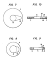
- Fig. 8 is a plan view of the first radiation/convection shielding plate 6.
- the plate is made of a carbon disk having a diameter of 250 mm.
- the plate is provided in the center with a hole 17 through which an upper shaft 12 is passed, and an inspection window 18 that is made continuous to said hole 17.
- hole 17 has a diameter of 120 mm.
- the edge of the-inspection window 18 is spaced from the circumference of the disk by a distance of 25 mm.
- the inspection window 18 is shown as a simple opening.
- that part of the plate 6 which corresponds to window 18 may be inlaid with a quartz plate 25 while the hole 17 is left open.
- a section of the plate 6 according to this modified embodiment is shown in Fig. 9.
- a better result will be obtained by evaporating a thin Au film 26 on the quartz plate so as to prevent Si leakage from that plate. The operator can observe the growth of a crystal through the translucent Au film 26. Furthermore, heat loss due to radiation can be inhibited by the Au film 26 which reflects almost all of infrared rays that fall on the plate 6.
- the tube 5 is made of carbon and has an inside diameter of 280 mm, an outside diameter of 340 mm and a height of 100 mm.
- the second shielding tube 5 is provided on the top with a disk-shaped secondary radiation/convection shielding plate 7. Again, the center of the second shielding plate 7 is provided with a hole through which the upper shaft 12 is to pass; the second shielding plate 7 is also provided with an inspection window that is continuous to the hole 19.
- a plan view of the second shielding plate 7 is shown in Fig. 7. In the embodiment shown, the hole 19 has a diameter of 100 mm.
- window 20 may effectively be closed by a quartz plate 25 with an evaporated Au film 26.
- a cross section of this modified embodiment is shown in Fig. 10.
- the crucible 4 contains a compound melt 8 and a liquid B203 encapsulant 14 that covers said melt.
- a seed crystal 13 is attached to the lower end of an upper shaft 12 hung from the top of a chamber 9, and as the upper shaft 12 is lifted, a GaAs crystal 10 is pulled upward following the movement of the seed crystal 13.
- the underside of the bottom of the susceptor 3 is provided with a supporting lower shaft 11.
- Each of the upper shaft 12 and lower shaft 11 is disposed in a vertically slidable and rotatable manner.
- Each shaft has suitable rotary seals where it passes through the chamber wall.
- a high pressure can be maintained within the chamber 9 by supplying a suitable gas such as an inert gas.
- a suitable gas such as an inert gas.
- nitrogen gas may be introduced into the chamber to hold the internal pressure to at least 10 atmospheres.
- a quartz rod 22 is inserted into the top of chamber 9 at an angle with respect to the longitudinal axis. This quartz rod also serves as an inspection window and has typically a diameter of 50 mm. Through inspection windows 22, 20 and 18, the operator can observe the compound melt 8 and the GaAs crystal 10 as it is withdrawn upward from the melt surface.
- the chamber 9 has an access door or means of opening (not shown) and suitable sealing means to prevent pressure loss.
- the apparatus of the present invention differs from the usual Czochralski pulling apparatus in at least the following two respects: it has upper and lower heaters 1 and 2; the radiation/ convection shielding tubes 16 and 5 and radiation/convection shielding plates 6 and 7 provide double shielding from the atmosphere in the space above the heaters so as to ensure minimum occurrence of heat radiation and convection.
- the cooling of the single crystal being pulled starts in the vicinity of the melt.
- lattice defects occur in the single crystal because that part of the crystal which is close to the melt is rapidly cooled.
- the mechanism by which the single crystal is cooled involves three factors, radiation, convection and conduction. Heat conduction through the upper shaft is negligible. The other factors, convection and radiation, are the primary causes of the cooling of the crystal.
- the apparatus of the present invention has two sets of radiation/convection shielding plate and tube. The gap between the first shielding tube 16 and the heater 1 is sufficiently small to inhibit convection. Since the crystal is heated to high temperature, heat loss due to radiation would be the most significant factor. Black body radiation is proportional to the fourth power of the absolute temperature.
- the first radiation/convection shielding plate 6 has hole 17 and inspection window 18, whereas the second shielding plate 7 has hole 19 and inspection window 20.
- the solid angle subtended by hole 1 9 and window 20 is smaller than that subtended by hole 17 and window 18, so the radiation loss occurring in the apparatus of the present invention is determined by the second radiation/convection shielding plate 7.
- the sum of the surface areas of hole 19 and inspection window 20 in the second shielding plate 7 shown in Fig. 6 is about 140 cm 2 .
- the vertical distance between the solid-liquid interface and the hole 19 and window 20 in the plate 7 is about 30 cm, so the solid angle subtended by 19 and 20 is 0.16 steradians.
- the solid angle subtended by an opening through which heat radiates is preferably smaller than 0.3 steradians.
- Three sets of a radiation/convection shielding plate and a shielding tube are preferably employed for the purpose of ensuring an even better uniformity in the temperature distribution across the crystal.
- a third set is indicated in Fig. 6 by the dashed line.
- the desired crystal can be pulled upward both by inspection through the window and by checking a weight change as sensed by a weight signal detector attached to the upper shaft.
- the apparatus of the present invention may be used to pull a B, Sb or In doped GaAs single crystal by direct synthesis.
- Direct synthesis is a method using elemental Ga and As, not polycrystalline GaAs as starting materials.
- Gallium, arsenic and an impurity B, Sb or In are first placed in the crucible.
- the number of moles of As should be larger than the number of moles of Ga in combination with In or B because some part of As will be lost by evaporation.
- B 2 0 3 is added to the mixture of Ga, As and the impurity.
- the respective components are melted at a temperature of 800°C or higher and at a pressure of 50 atm. or higher. As a result, a solid solution of GaAs containing indium is synthesized.
- the melt of GaAs is further heated by heaters 1 and 2 so as to provide a constant temperature gradient in the neighborhood of the melt surface.
- the tip of the seed crystal 13 on the lower shaft 12 is dipped in the surface of the melt and pulled upward with rotation.
- the seed crystal preferably has a direction ⁇ 100>.
- necking method may be performed, by which the diameter of a GaAs crystal that follows the seed crystal is reduced sufficiently to dispel the dislocations to the outside of the crystal. Subsequently, the diameter of the GaAs crystal is gradually increased to form a shoulder which grows to a predetermined diameter. In the subsequent period of the pulling operation,the diameter of the single-crystal ingot is held constant.
- the apparatus of the present invention is capable of growing GaAs single crystals having a diameter of at least 2 inches, sometimes 3 inches.
- the other conditions for pulling GaAs single crystals with the apparatus of the present invention are listed below:
- the upper and lower shafts rotate in the same direction or in the counter direction.
- a solid solution of indium-containing GaAs was synthesized from elementary Ga, As and In each having a purity of 99.9999%.
- the respective elements were charged in the crucible in the following amounts:
- the number of moles of indium taken together with gallium was smaller than that of arsenic by 0.36 moles.
- the GaAs single crystal pulled was in a generally cylindrical shape. It was about 180 mm long (as between the top of the shoulder and the bottom) and about 76 mm (3 inches) across. The area of the crystal where transition from the shoulder to the side wall of the cylindrical portion occurred was found to have 4.2 x 10 19 atoms of indium per cm 3 .
- the crystal pulled was single-crystal throughout the all length.
- a thin wafer was sliced from the single-crystal ingot. The wafer was polished and etched in preparation for EPD counting. Minimum EPD was less than 1000 cm-3, and in most areas of the wafer, EPD was between 3000 and 10,000cm -3 .
- the wafer had a specific resistivity in the range of 2 x 10 7 to 5 x 10 7 ohms-cm. One may well consider the wafer as a semi-insulator.
- the pulling apparatus of the present invention has the following advantages:
Landscapes
- Chemical & Material Sciences (AREA)
- Engineering & Computer Science (AREA)
- Crystallography & Structural Chemistry (AREA)
- Materials Engineering (AREA)
- Metallurgy (AREA)
- Organic Chemistry (AREA)
- Crystals, And After-Treatments Of Crystals (AREA)
- Liquid Deposition Of Substances Of Which Semiconductor Devices Are Composed (AREA)
Applications Claiming Priority (2)
| Application Number | Priority Date | Filing Date | Title |
|---|---|---|---|
| JP58227305A JP2553485B2 (ja) | 1983-11-30 | 1983-11-30 | 砒化ガリウム単結晶の製造方法 |
| JP227305/83 | 1983-11-30 |
Publications (3)
| Publication Number | Publication Date |
|---|---|
| EP0148396A2 true EP0148396A2 (de) | 1985-07-17 |
| EP0148396A3 EP0148396A3 (en) | 1987-07-22 |
| EP0148396B1 EP0148396B1 (de) | 1990-02-07 |
Family
ID=16858723
Family Applications (1)
| Application Number | Title | Priority Date | Filing Date |
|---|---|---|---|
| EP19840114480 Expired EP0148396B1 (de) | 1983-11-30 | 1984-11-29 | Vorrichtung zur Herstellung von einkristallinem Galliumarsenid und einkristallines Galliumarsenid hergestellt durch diese Vorrichtung |
Country Status (4)
| Country | Link |
|---|---|
| EP (1) | EP0148396B1 (de) |
| JP (1) | JP2553485B2 (de) |
| CA (1) | CA1254818A (de) |
| DE (1) | DE3481324D1 (de) |
Cited By (3)
| Publication number | Priority date | Publication date | Assignee | Title |
|---|---|---|---|---|
| RU2227821C1 (ru) * | 2003-04-29 | 2004-04-27 | Блецкан Николай Иванович | Устройство для выращивания монокристаллов сапфира |
| WO2004055249A1 (ja) * | 2002-12-18 | 2004-07-01 | Nikko Materials Co., Ltd. | 化合物半導体単結晶の製造方法および結晶成長装置 |
| CN114808131A (zh) * | 2022-04-20 | 2022-07-29 | 北京通美晶体技术股份有限公司 | 一种GaAs单晶及其VGF制备方法 |
Families Citing this family (4)
| Publication number | Priority date | Publication date | Assignee | Title |
|---|---|---|---|---|
| JP2517092B2 (ja) * | 1988-12-28 | 1996-07-24 | 三菱化学株式会社 | 単結晶成長方法 |
| EP0509312B1 (de) * | 1991-04-16 | 1995-08-23 | Sumitomo Electric Industries, Limited | Czochralsky-Verfahren unter Verwendung eines Bauelementes zum Abschirmen der Strahlung der Rohmaterial-Schmelzlösung und Vorrichtung hierfür |
| JP2795036B2 (ja) * | 1992-02-04 | 1998-09-10 | 信越半導体株式会社 | 単結晶引上装置 |
| KR101530272B1 (ko) * | 2013-08-07 | 2015-06-23 | 주식회사 엘지실트론 | 잉곳성장장치 및 잉곳성장방법 |
Family Cites Families (8)
| Publication number | Priority date | Publication date | Assignee | Title |
|---|---|---|---|---|
| JPS5912639B2 (ja) * | 1975-07-18 | 1984-03-24 | 日本電気株式会社 | 結晶成長法 |
| JPS57135794A (en) * | 1981-02-09 | 1982-08-21 | Nec Corp | Method of growing crystal of low-melting oxide |
| JPS57149900A (en) * | 1981-03-11 | 1982-09-16 | Nippon Telegr & Teleph Corp <Ntt> | Manufacture of gaas single crystal |
| JPS5895699A (ja) * | 1981-12-03 | 1983-06-07 | Nec Corp | Gaas単結晶の育成方法 |
| JPS58172291A (ja) * | 1982-03-31 | 1983-10-11 | Sumitomo Electric Ind Ltd | 化合物半導体単結晶の製造方法 |
| JPS58217492A (ja) * | 1982-06-08 | 1983-12-17 | Hitachi Metals Ltd | 結晶成長装置 |
| JPS59190293A (ja) * | 1983-04-11 | 1984-10-29 | Tohoku Metal Ind Ltd | 単結晶育成装置 |
| JPS6046998A (ja) * | 1983-08-26 | 1985-03-14 | Sumitomo Electric Ind Ltd | 単結晶引上方法及びそのための装置 |
-
1983
- 1983-11-30 JP JP58227305A patent/JP2553485B2/ja not_active Expired - Lifetime
-
1984
- 1984-11-28 CA CA000468860A patent/CA1254818A/en not_active Expired
- 1984-11-29 EP EP19840114480 patent/EP0148396B1/de not_active Expired
- 1984-11-29 DE DE8484114480T patent/DE3481324D1/de not_active Expired - Lifetime
Cited By (3)
| Publication number | Priority date | Publication date | Assignee | Title |
|---|---|---|---|---|
| WO2004055249A1 (ja) * | 2002-12-18 | 2004-07-01 | Nikko Materials Co., Ltd. | 化合物半導体単結晶の製造方法および結晶成長装置 |
| RU2227821C1 (ru) * | 2003-04-29 | 2004-04-27 | Блецкан Николай Иванович | Устройство для выращивания монокристаллов сапфира |
| CN114808131A (zh) * | 2022-04-20 | 2022-07-29 | 北京通美晶体技术股份有限公司 | 一种GaAs单晶及其VGF制备方法 |
Also Published As
| Publication number | Publication date |
|---|---|
| JPS60118699A (ja) | 1985-06-26 |
| EP0148396A3 (en) | 1987-07-22 |
| JP2553485B2 (ja) | 1996-11-13 |
| DE3481324D1 (de) | 1990-03-15 |
| EP0148396B1 (de) | 1990-02-07 |
| CA1254818A (en) | 1989-05-30 |
Similar Documents
| Publication | Publication Date | Title |
|---|---|---|
| Bass et al. | Pulling of gallium phosphide crystals by liquid encapsulation | |
| US3716345A (en) | Czochralski crystallization of gallium arsenide using a boron oxide sealed device | |
| Földvári et al. | Growth and properties of Bi2TeO5 single crystals | |
| US3849205A (en) | Enhancement of solid state recrystallization by induced nucleation | |
| Leverton | Floating crucible technique for growing uniformly doped crystals | |
| Ainsworth | Single crystal bismuth telluride | |
| Triboulet | CdTe And CdTe: Hg alloys crystal growth using stoichiometric and off-stoichiometric zone passing techniques | |
| EP0148396B1 (de) | Vorrichtung zur Herstellung von einkristallinem Galliumarsenid und einkristallines Galliumarsenid hergestellt durch diese Vorrichtung | |
| Barz et al. | Germanium-rich SiGe bulk single crystals grown by the vertical Bridgman method and by zone melting | |
| Wagner | Preparation and properties of bulk In1− x Ga x As alloys | |
| Iseler | Liquid-encapsulated Czochralski growth of InP crystals | |
| JPH0448759B2 (de) | ||
| Wald et al. | Crystal growth of CdTe for γ-ray detectors | |
| Woodbury et al. | Improved sealed-ingot zone refining technique for growth of CdTe crystals | |
| Nail et al. | Preparation of Silver Halide Crystals of High Purity | |
| Mullin et al. | The melt-growth and characterization of cadmium telluride | |
| Carruthers | Crystal growth from the melt | |
| US3242015A (en) | Apparatus and method for producing single crystal structures | |
| Dutta et al. | Segregation of tellurium in GaSb single crystals and associated diffusion coefficient in the solute layer | |
| Iseler | Advances in LEC growth of InP crystals | |
| Vohl | Synthesis and crystal growth of CdGeP2 | |
| Kremer et al. | Composition gradients and segregation in Hg1− xMnxTe | |
| Blum et al. | Growth of large single crystals of gallium phosphide from a stoichiometric melt | |
| Gürbulak | Growth and absorption properties of Dy-doped and undoped p-type TlGaSe2 | |
| Maeta et al. | A low-temperature glass cryostat for X-ray diffraction work |
Legal Events
| Date | Code | Title | Description |
|---|---|---|---|
| PUAI | Public reference made under article 153(3) epc to a published international application that has entered the european phase |
Free format text: ORIGINAL CODE: 0009012 |
|
| AK | Designated contracting states |
Designated state(s): DE FR GB |
|
| PUAL | Search report despatched |
Free format text: ORIGINAL CODE: 0009013 |
|
| AK | Designated contracting states |
Kind code of ref document: A3 Designated state(s): DE FR GB |
|
| 17P | Request for examination filed |
Effective date: 19870814 |
|
| 17Q | First examination report despatched |
Effective date: 19880607 |
|
| GRAA | (expected) grant |
Free format text: ORIGINAL CODE: 0009210 |
|
| AK | Designated contracting states |
Kind code of ref document: B1 Designated state(s): DE FR GB |
|
| ET | Fr: translation filed | ||
| REF | Corresponds to: |
Ref document number: 3481324 Country of ref document: DE Date of ref document: 19900315 |
|
| PLBE | No opposition filed within time limit |
Free format text: ORIGINAL CODE: 0009261 |
|
| STAA | Information on the status of an ep patent application or granted ep patent |
Free format text: STATUS: NO OPPOSITION FILED WITHIN TIME LIMIT |
|
| 26N | No opposition filed | ||
| PGFP | Annual fee paid to national office [announced via postgrant information from national office to epo] |
Ref country code: FR Payment date: 19981110 Year of fee payment: 15 |
|
| PGFP | Annual fee paid to national office [announced via postgrant information from national office to epo] |
Ref country code: GB Payment date: 19981204 Year of fee payment: 15 |
|
| PGFP | Annual fee paid to national office [announced via postgrant information from national office to epo] |
Ref country code: DE Payment date: 19981207 Year of fee payment: 15 |
|
| REG | Reference to a national code |
Ref country code: GB Ref legal event code: 746 Effective date: 19990614 |
|
| PG25 | Lapsed in a contracting state [announced via postgrant information from national office to epo] |
Ref country code: GB Free format text: LAPSE BECAUSE OF NON-PAYMENT OF DUE FEES Effective date: 19991129 |
|
| GBPC | Gb: european patent ceased through non-payment of renewal fee |
Effective date: 19991129 |
|
| PG25 | Lapsed in a contracting state [announced via postgrant information from national office to epo] |
Ref country code: FR Free format text: LAPSE BECAUSE OF NON-PAYMENT OF DUE FEES Effective date: 20000731 |
|
| PG25 | Lapsed in a contracting state [announced via postgrant information from national office to epo] |
Ref country code: DE Free format text: LAPSE BECAUSE OF NON-PAYMENT OF DUE FEES Effective date: 20000901 |
|
| REG | Reference to a national code |
Ref country code: FR Ref legal event code: ST |