EP0148771A2 - Détecteur de proximité capacitif - Google Patents
Détecteur de proximité capacitif Download PDFInfo
- Publication number
- EP0148771A2 EP0148771A2 EP85300098A EP85300098A EP0148771A2 EP 0148771 A2 EP0148771 A2 EP 0148771A2 EP 85300098 A EP85300098 A EP 85300098A EP 85300098 A EP85300098 A EP 85300098A EP 0148771 A2 EP0148771 A2 EP 0148771A2
- Authority
- EP
- European Patent Office
- Prior art keywords
- gain amplifier
- unity gain
- input
- output
- coupled
- Prior art date
- Legal status (The legal status is an assumption and is not a legal conclusion. Google has not performed a legal analysis and makes no representation as to the accuracy of the status listed.)
- Granted
Links
- 239000004020 conductor Substances 0.000 claims abstract description 27
- 238000001514 detection method Methods 0.000 claims abstract description 3
- 238000000034 method Methods 0.000 claims description 2
- 230000008878 coupling Effects 0.000 claims 4
- 238000010168 coupling process Methods 0.000 claims 4
- 238000005859 coupling reaction Methods 0.000 claims 4
- 230000003071 parasitic effect Effects 0.000 description 9
- 230000005540 biological transmission Effects 0.000 description 2
- 230000000694 effects Effects 0.000 description 2
- 238000012986 modification Methods 0.000 description 2
- 230000004048 modification Effects 0.000 description 2
- 239000004065 semiconductor Substances 0.000 description 2
- 230000002411 adverse Effects 0.000 description 1
- 230000003321 amplification Effects 0.000 description 1
- 238000010586 diagram Methods 0.000 description 1
- 238000004519 manufacturing process Methods 0.000 description 1
- 239000000463 material Substances 0.000 description 1
- 238000006386 neutralization reaction Methods 0.000 description 1
- 238000003199 nucleic acid amplification method Methods 0.000 description 1
- 230000003287 optical effect Effects 0.000 description 1
Images
Classifications
-
- H—ELECTRICITY
- H03—ELECTRONIC CIRCUITRY
- H03F—AMPLIFIERS
- H03F1/00—Details of amplifiers with only discharge tubes, only semiconductor devices or only unspecified devices as amplifying elements
- H03F1/08—Modifications of amplifiers to reduce detrimental influences of internal impedances of amplifying elements
- H03F1/14—Modifications of amplifiers to reduce detrimental influences of internal impedances of amplifying elements by use of neutralising means
-
- H—ELECTRICITY
- H03—ELECTRONIC CIRCUITRY
- H03F—AMPLIFIERS
- H03F3/00—Amplifiers with only discharge tubes or only semiconductor devices as amplifying elements
- H03F3/50—Amplifiers in which input is applied to, or output is derived from, an impedance common to input and output circuits of the amplifying element, e.g. cathode follower
Definitions
- This invention relates in general to amplifiers and more particularly to amplifier circuits having means for minimizing the input-capacitance thereof. Still more particularly, this invention relates to amplifier circuitry useful in driving the guard shield of a highly sensitive proximity sensor which operates by detection of varying capacitance at a remotely disposed sense electrode.
- Proximity sensors are well known in the prior art. Such systems often operate by utilizing magnetic or optical detectors which generate a signal in response to the presence or absence of an object. More recently, capacitive proximity sensors have been utilized which use a high impedance AC signal to detect variations in the capacitive loading of the AC signal due to the presence of an object. However, these capacitive proximity sensors suffer from a severe shortcoming in that small variations in parasitic capacitance in the associated electronic circuitry may cause faulty indications. Typically, these systems are sensitive to capacitive variations at the sense electrode on the order of .005 picoFarads. Thus, those skilled in the art will appreciate that parasitic capacitance can generate a major problem when present in the associated circuitry utilized with a proximity sensor of this type.
- a second shortcoming of these capacitive proximity sensors is also related to the highly susceptible nature of the high impedance AC signal utilized. It is often necessary to dispose the electronic circuitry associated with these sensors at some distance from the sense electrode itself due to an adverse or hostile environment in which an object must be sensed. Examples of this situation include the various hostile environments to which a semiconductor wafer must be exposed during fabrication.
- the necessity of utilizing remote sense electrodes generates a second problem with the stray capacitance found in most electrical transmission lines.
- the approach typically utilized in the prior art to solve this problem is to drive an outer conductor or "guard shield" with an amplified version of the signal being guarded. This maintains both the inner conductor and the guard shield at identical electrical potentials and minimizes the capacitance in the transmission line.
- the necessity of amplification introduces additional electronic circuitry which necessarily includes additional parasitic capacitance.
- a low input-capacitance amplifier is provided for utilization in driving a guard shield of a high impedance AC signal.
- the high impedance AC signal is applied to a central conductor and to the input of a first unity gain amplifier.
- the output of that unity gain amplifier is applied to a second unity gain amplifier which is utilized to provide the guard signal to the shield conductor and also to provide electrical power to the first unity gain amplifier.
- a preferred embodiment of the present invention is utilized in conjunction with a highly sensitive capacitance proximity sensor which has a sense electrode remotely located from the associated electronic circuitry.
- the output and all electrical power receiving nodes are maintained at substantially identical AC electrical potentials thereby nullifying the loading effect of any parasitic capacitances at the input of the first amplifier circuitry.
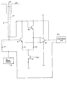
- AC signal source 10 is utilized to provide an AC signal which is coupled to one input of phase and magnitude comparison circuit 16 and through high impedance resistor 11 to inner conductor 12 and to the base of transistor 14.
- phase and magnitude comparison circuit 16 is coupled to one input of phase and magnitude comparison circuit 16 and through high impedance resistor 11 to inner conductor 12 and to the base of transistor 14.
- resistor 11 is coupled to one input of phase and magnitude comparison circuit 16 and through high impedance resistor 11 to inner conductor 12 and to the base of transistor 14.
- the depicted circuit is somewhat simplified in nature and that various filters, level adjusting circuits and other circuit elements will normally be interposed between AC signal source 10 and phase and magnitude comparison circuit 16.
- inner conductor 12 is shielded by an outer coaxial conductor 18 and is coupled at a second end thereof to a remote sense electrode 20 which is disposed within a sensor assembly 22.
- sensor assembly 22 will typically be built into a machine and that multiple sense electrodes may be utilized with a single material handling machine.
- the high impedance AC signal is coupled to the base of transistor 14.
- transistor 14 is coupled in an emitter follower configuration and will thus function as a unity gain amplifier.
- the emitter bias current of transistor 14 is determined by a constant current regulator which is provided by transistor 28, which has a reference voltage applied to the base thereof.
- the output of the unity gain amplifier is taken at the emitter of transistor 14 and is applied to the noninverting input of amplifier 26, a standard operational amplifier which is also configured for unity gain.
- the output of operational amplifier 26 is then coupled back to coaxial conductor 18 and to the collector of transistor 14.
- phase and magnitude comparison circuit 16 which is utilized to detect those changes in phase and magnitude of the AC signal which will occur in response to the presence of an object at or near sense electrode 20.
- the capacitance sensitive signal which is applied to the base of transistor 14 is not degraded by the parasitic capacitance of the transistor amplifier circuit because each of the transistor's terminals are experiencing an identical AC signal.
- the emitter-to-base capacitance, C eb does not load the sensitive signal because of the nature of an emitter follower, in that the emitter voltage closely tracks the base voltage with only a small DC offset.
- the collector-to-base capacitance C cb is minimized because the collector is driven by the output of operational amplifier 26 and experiences the same AC voltage as the emitter and base.
- transistor 32 is coupled in diode configuration between the output of operational amplifier 26 and the inverting input terminal thereof.
- Transistor 32 is chosen to have matched characteristics with transistor 14 and is coupled in a diode configuration having its collector and base both tied to the output of operational amplifier 26.
- the emitter bias current of transistor 32 is also determined by the constant current source formed by transistor 28.
- Resistors 24 and 30 are chosen to be equal in resistance so that an identical amount of current flows through transistors 32 and 14, thus ensuring an equal voltage drop across these transistors. Because of the presence of transistor 32 coupled in this manner, the collector of transistor 14 is offset in DC voltage from the voltage at the emitter. This offset will be equal to one diode drop.
- transistor 14 With the collector of transistor 14 one diode drop higher than its emitter, transistor 14 will operate in its active region. And, since the base of transistor 14 is forward biased and one diode drop higher in voltage than the emitter, the base and collector of transistor 14, and the input and output of the entire circuit are at very nearly the same DC voltage.
- the DC offset function performed by transistor 32 may also be performed by utilizing a diode or other DC level shifting device.
Landscapes
- Engineering & Computer Science (AREA)
- Power Engineering (AREA)
- Electronic Switches (AREA)
- Amplifiers (AREA)
Applications Claiming Priority (2)
| Application Number | Priority Date | Filing Date | Title |
|---|---|---|---|
| US56866684A | 1984-01-06 | 1984-01-06 | |
| US568666 | 1984-01-06 |
Publications (3)
| Publication Number | Publication Date |
|---|---|
| EP0148771A2 true EP0148771A2 (fr) | 1985-07-17 |
| EP0148771A3 EP0148771A3 (en) | 1985-08-28 |
| EP0148771B1 EP0148771B1 (fr) | 1989-04-12 |
Family
ID=24272223
Family Applications (1)
| Application Number | Title | Priority Date | Filing Date |
|---|---|---|---|
| EP19850300098 Expired EP0148771B1 (fr) | 1984-01-06 | 1985-01-07 | Détecteur de proximité capacitif |
Country Status (2)
| Country | Link |
|---|---|
| EP (1) | EP0148771B1 (fr) |
| DE (1) | DE3569445D1 (fr) |
Cited By (2)
| Publication number | Priority date | Publication date | Assignee | Title |
|---|---|---|---|---|
| GB2271642A (en) * | 1992-10-19 | 1994-04-20 | De La Rue Syst | Conductive strip detector |
| JP2006084318A (ja) * | 2004-09-16 | 2006-03-30 | Oki Electric Ind Co Ltd | 静電容量型距離センサ |
-
1985
- 1985-01-07 EP EP19850300098 patent/EP0148771B1/fr not_active Expired
- 1985-01-07 DE DE8585300098T patent/DE3569445D1/de not_active Expired
Non-Patent Citations (4)
| Title |
|---|
| ELECTRONICS, vol. 50, no. 2, 20th January 1977, pages 112-113, New York, US; M.V. THOMAS: "Input capacitance feedback improves neutralization" * |
| IBM TECHNICAL DISCLOSURE BULLETIN, vol. 9, no. 11, April 1967, page 1657, New York, US; A.R. BERDING: "Low-input capacitance isolating circuit" * |
| IEEE JOURNAL OF SOLID-STATE CIRCUITS, vol. SC-12, no. 3, June 1977, pages 217-224, New York, US; H.J. DE MAN et al.: "A low input capacitance voltage follower in a compatible silicon-gate MOS-bipolar technology" * |
| TOUTE L'ELECTRONIQUE, no. 439, January 1979, page 45, Paris, FR; "Amplificateur à très faible capacité d'entrée" * |
Cited By (4)
| Publication number | Priority date | Publication date | Assignee | Title |
|---|---|---|---|---|
| GB2271642A (en) * | 1992-10-19 | 1994-04-20 | De La Rue Syst | Conductive strip detector |
| GB2271642B (en) * | 1992-10-19 | 1996-06-05 | De La Rue Syst | Conductive strip detector |
| US5650729A (en) * | 1992-10-19 | 1997-07-22 | De La Rue Systems Limited | Conductive strip detector |
| JP2006084318A (ja) * | 2004-09-16 | 2006-03-30 | Oki Electric Ind Co Ltd | 静電容量型距離センサ |
Also Published As
| Publication number | Publication date |
|---|---|
| EP0148771B1 (fr) | 1989-04-12 |
| DE3569445D1 (en) | 1989-05-18 |
| EP0148771A3 (en) | 1985-08-28 |
Similar Documents
| Publication | Publication Date | Title |
|---|---|---|
| JP3135283B2 (ja) | 絶対値検出用信号処理回路装置 | |
| US5442347A (en) | Double-driven shield capacitive type proximity sensor | |
| US6373236B1 (en) | Temperature compensated power detector | |
| US5371469A (en) | Constant current loop impedance measuring system that is immune to the effects of parasitic impedances | |
| US4853639A (en) | Non-contacting voltage metering apparatus | |
| US4795905A (en) | Circuit layout for an infrared room surveillance detector | |
| KR910009088B1 (ko) | 온도 안정 rf 검출기 | |
| US4176555A (en) | Signal amplifier system for controlled carrier signal measuring sensor/transducer of the variable impedance type | |
| US3622898A (en) | Circuit for processing hall generator output signals | |
| US5986456A (en) | Surface potential sensor and processing circuit having improved noise reduction | |
| US4626678A (en) | Light detecting circuit | |
| US7141910B2 (en) | Transconductance circuit for piezoelectric transducer | |
| US5079454A (en) | Temperature compensated FET power detector | |
| US4654603A (en) | Low input-capacitance amplifier for driving guard shield conductors | |
| AU2005234374B2 (en) | Transconductance circuit for piezoelectric transducer | |
| US5155449A (en) | FET buffer amplifier | |
| JPH11504774A (ja) | オフセット補償型リニアrf検出器 | |
| EP0148771A2 (fr) | Détecteur de proximité capacitif | |
| KR900000707A (ko) | 회로 소자 측정 장치 | |
| US4843344A (en) | High voltage amplifier | |
| JPS62100626A (ja) | 赤外線式室内監視検知器用回路装置 | |
| US6949977B2 (en) | Circuit arrangement having a transimpedance amplifier connected to a current limiter circuit | |
| US4935618A (en) | Wide bandwidth photoelectric converting circuit | |
| EP0266551A1 (fr) | Voltmètre sans contact | |
| JP3392090B2 (ja) | 信号検知装置 |
Legal Events
| Date | Code | Title | Description |
|---|---|---|---|
| PUAI | Public reference made under article 153(3) epc to a published international application that has entered the european phase |
Free format text: ORIGINAL CODE: 0009012 |
|
| PUAL | Search report despatched |
Free format text: ORIGINAL CODE: 0009013 |
|
| AK | Designated contracting states |
Designated state(s): CH DE FR GB LI NL |
|
| AK | Designated contracting states |
Designated state(s): CH DE FR GB LI NL |
|
| 17P | Request for examination filed |
Effective date: 19860227 |
|
| 17Q | First examination report despatched |
Effective date: 19870709 |
|
| GRAA | (expected) grant |
Free format text: ORIGINAL CODE: 0009210 |
|
| AK | Designated contracting states |
Kind code of ref document: B1 Designated state(s): CH DE FR GB LI NL |
|
| PG25 | Lapsed in a contracting state [announced via postgrant information from national office to epo] |
Ref country code: NL Effective date: 19890412 Ref country code: FR Free format text: THE PATENT HAS BEEN ANNULLED BY A DECISION OF A NATIONAL AUTHORITY Effective date: 19890412 |
|
| REF | Corresponds to: |
Ref document number: 3569445 Country of ref document: DE Date of ref document: 19890518 |
|
| EN | Fr: translation not filed | ||
| NLV1 | Nl: lapsed or annulled due to failure to fulfill the requirements of art. 29p and 29m of the patents act | ||
| PLBI | Opposition filed |
Free format text: ORIGINAL CODE: 0009260 |
|
| 26 | Opposition filed |
Opponent name: I F M ELECTRONIC GMBH Effective date: 19900112 |
|
| PLBN | Opposition rejected |
Free format text: ORIGINAL CODE: 0009273 |
|
| STAA | Information on the status of an ep patent application or granted ep patent |
Free format text: STATUS: OPPOSITION REJECTED |
|
| 27O | Opposition rejected |
Effective date: 19951201 |
|
| PGFP | Annual fee paid to national office [announced via postgrant information from national office to epo] |
Ref country code: GB Payment date: 20000105 Year of fee payment: 16 |
|
| PGFP | Annual fee paid to national office [announced via postgrant information from national office to epo] |
Ref country code: CH Payment date: 20000106 Year of fee payment: 16 |
|
| PG25 | Lapsed in a contracting state [announced via postgrant information from national office to epo] |
Ref country code: GB Free format text: LAPSE BECAUSE OF NON-PAYMENT OF DUE FEES Effective date: 20010107 |
|
| PG25 | Lapsed in a contracting state [announced via postgrant information from national office to epo] |
Ref country code: LI Free format text: LAPSE BECAUSE OF NON-PAYMENT OF DUE FEES Effective date: 20010131 Ref country code: CH Free format text: LAPSE BECAUSE OF NON-PAYMENT OF DUE FEES Effective date: 20010131 |
|
| GBPC | Gb: european patent ceased through non-payment of renewal fee |
Effective date: 20010107 |
|
| PGFP | Annual fee paid to national office [announced via postgrant information from national office to epo] |
Ref country code: DE Payment date: 20010831 Year of fee payment: 17 |
|
| REG | Reference to a national code |
Ref country code: CH Ref legal event code: PL |
|
| PG25 | Lapsed in a contracting state [announced via postgrant information from national office to epo] |
Ref country code: DE Free format text: LAPSE BECAUSE OF NON-PAYMENT OF DUE FEES Effective date: 20020801 |