EP0149511A2 - Circuit de mémoire pour un dispositif d'affichage - Google Patents
Circuit de mémoire pour un dispositif d'affichage Download PDFInfo
- Publication number
- EP0149511A2 EP0149511A2 EP85300029A EP85300029A EP0149511A2 EP 0149511 A2 EP0149511 A2 EP 0149511A2 EP 85300029 A EP85300029 A EP 85300029A EP 85300029 A EP85300029 A EP 85300029A EP 0149511 A2 EP0149511 A2 EP 0149511A2
- Authority
- EP
- European Patent Office
- Prior art keywords
- memory
- data
- display
- picture element
- bits
- Prior art date
- Legal status (The legal status is an assumption and is not a legal conclusion. Google has not performed a legal analysis and makes no representation as to the accuracy of the status listed.)
- Withdrawn
Links
Images


Classifications
-
- G—PHYSICS
- G06—COMPUTING OR CALCULATING; COUNTING
- G06F—ELECTRIC DIGITAL DATA PROCESSING
- G06F13/00—Interconnection of, or transfer of information or other signals between, memories, input/output devices or central processing units
- G06F13/14—Handling requests for interconnection or transfer
-
- G—PHYSICS
- G09—EDUCATION; CRYPTOGRAPHY; DISPLAY; ADVERTISING; SEALS
- G09G—ARRANGEMENTS OR CIRCUITS FOR CONTROL OF INDICATING DEVICES USING STATIC MEANS TO PRESENT VARIABLE INFORMATION
- G09G5/00—Control arrangements or circuits for visual indicators common to cathode-ray tube indicators and other visual indicators
- G09G5/02—Control arrangements or circuits for visual indicators common to cathode-ray tube indicators and other visual indicators characterised by the way in which colour is displayed
-
- G—PHYSICS
- G06—COMPUTING OR CALCULATING; COUNTING
- G06F—ELECTRIC DIGITAL DATA PROCESSING
- G06F12/00—Accessing, addressing or allocating within memory systems or architectures
-
- G—PHYSICS
- G09—EDUCATION; CRYPTOGRAPHY; DISPLAY; ADVERTISING; SEALS
- G09G—ARRANGEMENTS OR CIRCUITS FOR CONTROL OF INDICATING DEVICES USING STATIC MEANS TO PRESENT VARIABLE INFORMATION
- G09G5/00—Control arrangements or circuits for visual indicators common to cathode-ray tube indicators and other visual indicators
- G09G5/36—Control arrangements or circuits for visual indicators common to cathode-ray tube indicators and other visual indicators characterised by the display of a graphic pattern, e.g. using an all-points-addressable [APA] memory
- G09G5/39—Control of the bit-mapped memory
- G09G5/391—Resolution modifying circuits, e.g. variable screen formats
Definitions
- This invention relates to a digital computer.
- Dynamic random access semiconductor memory is commonly used in digital computers because integrated circuits using such memory can have a very much larger capacity than static random access semiconductor memory. This is because a static semiconductor memory requires at least two transistors for each bit and possibly more than that, whereas a dynamic memory needs only a single transistor per bit. Moreover, a static semiconductor memory requires more current for its operation because one of the transistors in each cell is conducting at all times, whereas in a dynamic memory cell the data is stored as a voltage on a capacitor. A disadvantage with dynamic semiconductor memory is that the charge on the capacitor must be refreshed periodically in order to ensure that the voltage on the capacitor has not decayed sufficiently to lead to corruption of the stored data. In a typical dynamic RAM chip 64 K memory cells are provided and these require to be refreshed every 2 ms.
- the refreshing of a dynamic RAM integrated circuit is effected by addressing all of the rows of the memory at least once in each 2 ms interval, the accessing of a row resulting in the data stored in all the elements in that row being applied to output amplifiers and rewritten in the elements again. It is not necessary for any data output to be produced during the refreshing operation.
- the advantages provided by dynamic RAMs of greater capacity and lower power consumption are considered to outweigh it.
- the use of dynamic RAM integrated circuits has become so widespread that certain microprocessors include dynamic RAM refreshment cycles in their operation sequences. Nevertheless, the disadvantage of having to provide for the refreshment of the data stored in the dynamic RAMs is an inconvenience which has to be allowed for in the design of a computer.
- a digital computer having dynamic random access semiconductor memory in which refreshing of the stored data is effected by periodically addressing each row of the memory and the computer is intended for use with display means including a raster scanned display device such as a cathode ray tube wherein data for display is stored in the memory in such locations that the reading of the data for display results in all the rows of memory being addressed at sufficiently short intervals to refresh the entire memory.
- display means including a raster scanned display device such as a cathode ray tube wherein data for display is stored in the memory in such locations that the reading of the data for display results in all the rows of memory being addressed at sufficiently short intervals to refresh the entire memory.
- the computer may include conversion means for converting data representing the coordinates of a position on the display to the memory address of the data to be displayed at that position.
- the conversion means which may include a multiplexer, may be connected in address bus lines between a central processing unit and the memory.
- the refreshing of the stored data may continue during part of the line and field flyback intervals.
- the data for display may be read from a plurality of columns of the memory with each row addressing operation and the data so read converted to serial form at a rate appropriate to the display.
- the central processing unit may be permitted access to the memory between successive row addressing operations used to provide data for display as well as during either or both flyback intervals.
- the display may have two modes, one having 512 pixels (picture elements) per line in which each pixel is defined by 2 bits of data, and the other having 256 pixels per line in which each pixel is defined by 4 bits of data,so that data is read from the memory at the same rate in both modes.
- a pixel is defined by 2 bits these may relate to green and red components respectively so that the 4 combinations of 2 bits give green, red, white and black for each pixel, white being achieved by arranging that if green and red are both present they also produce a blue output.
- a pixel is defined by 4 bits, one may be used to indicate the presence or absence of flashing at the pixel, and the other 3 bits respectively represent red, green and blue components and permit ihe pixel to have 6 colours in addition to black and white.
- raster scanned display means for a computer having a high resolution mode in which each picture element is defined by 2 bits and a low resolution mode in which each picture element is defined by a multiple of 2 bits so that the rate of data for display is the same in both modes, the 2 bits of a picture element in the high resolution modes respectively representing 2 primary colour components., and the means being such that it if both primary colour components are present the third primary colour component is also produced so that a white picture element is displayed.
- the computer includes a display interface for receiving the data for display and producing from them signals for application to the display device either directly or after further processing.
- This device may be a colour cathode ray tube monitor or a colour television receiver, in which latter case the further processing would include forming a colour television signal, for example according to the PAL, SECAM or NTS C system and modulating a suitable carrier with it.
- the display interface itself may be formed as a single integrated circuit using custom or semi-custom design techniques with standard cell or gate arrays.
- the computer has a peripheral interface for handling inputs to and outputs other than the display from the computer.
- This interface may also be constructed as a single integrated circuit.
- One of the inputs to the computer is from a keyboard and a further processor may be provided to handle the keyboard.
- the number of connections to the peripheral interface when in integrated circuit form the channel connecting the keyboard to the interface may be a serial link and this link may utilise a protocol such that only two conductors (apart from earth or ground) are required.
- a serial data link having two conductors in which a ready signal and the data are multiplexed on to one of the conductors and control signals are conveyed by the other conductor.
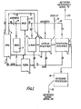
- FIG. 1 the example of a computer shown has a CPU 1 connected to an 8-wire data bus 2 and an 18-wire address bus 3. Two further wires 4 carrying control signals from the CPU are connected to a dynamic semiconductor random access memory 5 and a display interface 6.
- the data bus 2 is connected to a read-only memory 7 and a bus transmitter-receiver 8.
- the transmitter-receiver 8 acts as a buffer between the data bus 2 and a second 8-wire data bus 9 which is connected to the memory 5 and the interface 6 as well as a peripheral interface 10.
- the address bus 3 is divided into two parts of which a first part 11 having 16 wires is connected to ROM 7 and a multiplexer 12, and the second part 13 having 2 wires is connected to the display interface 6.
- the display interface 6 has an output 15 for connection to a display device which may be a monochrome or colour monitor or television receiver; it is assumed that the display device will be a colour monitor to which red, green and blue video signals can be applied, a television receiver being usable if the colour video signals are processed to a standard colour television signal form and modulated on a suitable carrier.
- the display interface 6 also produces some control signals on a channel 16 which conveys the signals to the CPU 1, the transmitter-receiver 8 and the multiplexer 12.
- the peripheral interface 10 is connected through a 2-wire serial link 17 to a keyboard processor 18 having a channel 19 for connection to a keyboard and for other purposes to be described in more detail later.
- the peripheral interface 10 has a second output 20 which is connectible to a network interface, to large capacity magnetic tape data stores known as micro- drives and to an interface for transmission of a serial data signal according to, for example the RS-232-C format.
- the channel 19 is connectible to a receiving interface for an RS-232-C signal and can also be connected to a sound reproducing device such as a loudspeaker.
- the CPU 1 in the particular example is a microprocessor of type 68008 manufactured by Motorola i.a. which has connections for an 8-bit data bus and a 20-bit address bus. Only 18 of the address bus connections are used in the example described, the other two connections are available for expansion of the memory capacity.
- the memory 5 has a capacity of 128 K bytes and is constructed from 16 64 K RAM integrated circuits. Such integrated circuits have an 8-bit address input to which 8-bit row and column addresses are applied in turn using row and column address strobes to activate the response of the circuit to the row and column address inputs. These row and column address signals are generated by the display interface 6 in response to control signals applied to it from the CPU 1 via the control lines 4.
- the interface 6 also responds to the address data received directly from the CPU 1 via the 2-wire bus 13 to determine to which of the two groups of 8 RAM chips in the memory 5 the row and column address strobes are to be applied.
- the display interface 6 and the peripheral interface 10 may be constructed as single integrated circuits using standard cell or ULA techniques.
- the keyboard processor is of the type 8049 produced by Intel and is programmed to perform the keyboard scanning and other functions required of it.
- Figure 2 shows the time diagram of the display produced by the computer.
- This diagram corresponds to a 312 line 50 Hz non-interlaced television picture which could be reproduced by a conventional 625 line television receiver.
- the width of the outer rectangle 100 represents 64 ⁇ s and its height 20 ms.
- a major part bounded by lines 101 represents the active display and the L-shaped region outside this represents the line and field flyback intervals.
- the data for display is stored in part of the memory 5 and is transferred from it via the data bus 9 to the display interface 6 and from that through the output 15 to the display.
- the 128 K bytes of storage in the memory 5 one- quarter, that is to say 32 K bytes, is allocated to the storage of the data for display.
- This memory space is arranged to occupy half of the columns of one set of the 64 K RAM IC's so that in reading the data for display from the memory 5, which reading is performed as required by the timing of the display itself, all of the rows of the memory 5 are addressed. Since the memory 5 is constructed from dynamic semiconductor memory it is necessary for all of the rows to be addressed at intervals of about 2 ms to refresh the stored data. As shown in Figure 2, the row addresses are distributed in groups of 8 over 32 lines of the display, the row addresses being set out in Figure 2 in hexadecimal form so that the 256 addresses of the rows extend from 0 to FF.
- the row addresses 0 to 7 are accessed four times in cyclic succession and may be addressed for a fifth time during the line flyback period.
- row addresses 8 to F are accessed and so on as shown.
- the 32 lines during which all of the rows of the memory 5 are addressed occupy about 2 ms so that the addressing of the memory 5 to produce the display from the stored data satisfies the requirements for refreshing the memory. It will be clear that all of the rows of the memory are addressed 32 times during the active display. Since the field flyback period is slightly more than 2 ms in duration, the cyclic addressing of the rows of the memory continues for refreshing the data only during the first fifth of each line during the field flyback interval. Since there is not sufficient time during the field flyback interval to complete the addressing of all of the rows of the memory twice, such memories as can be addressed twice are and those from which there is not sufficient time are not addressed.
- the display itself has two resolutions, a high resolution with 512 pixels (picture elements) per line and a low resolution with 256 pixels per line.
- a high resolution with 512 pixels (picture elements) per line
- a low resolution with 256 pixels per line.
- it folbws that 4 bytes are read from the memory by addressing 4 columns in turn during each row address operation producing 4 bytes of data for 16 pixels at high resolution allowing 2 bits per pixel or for 8 pixels at low resolution allowing 4 bits per pixel.
- the mapping of the picture elements over the memory addresses is fairly complicated. Since it is frequently required to be able to produce a particular display at a particular location on the display area, it is desirable that the relationship between the locations on the display and the memory addresses is apparently simplified as far as the user is concerned and this is achieved in the example of the computer shown by arranging that the lines of the address bus 11 are connected in such a manner to the multiplexer 12 so as to make it appear to the user that the memory addresses correspond to the coordinates of the locations on the display.
- the lines of the address bus 11 if numbered AO to A15 are connected to the inputs of the multiplexer 12 in the following order: A2, AO, A3, Al, A4, A5, A7, A6, A8, A12, A9, A13, A10, A14, All, A15.
- the multiplexer is arranged to select alternate inputs for connection to the bus 14 and then the intervening inputs.
- Figure 3 shows in some more detail the memory 5 and the generation of the signals for producing the display from the stored data.
- the memory is represented by the rectangle 200 and has a 256 output row driver 201 and 512 input column selector 202.
- 4 bytes of data are read by addressing in succession 4 columns of the memory.
- the 4 bytes are conveyed via the data bus 9 to the display interface 6 where the first 2 bytes are stored in registers 203 and 204 and then immediately transferred to a 16-bit shifting register 205 so that the registers 203 and 204 are able to receive the second 2 bytes.
- the 16 bits stored in the shifting register 205 are stepped out at a rate compatible with the display to be produced and then when all of the first 2 bytes have been shifted out the second 2 bytes are transferred in the register 205 to continue with the output.
- the interval of time necessary to read the data from the memory is shorter than the interval of time over which that data is distributed to produce the display, there is a short period between the reading of the data for display from the memory during which the CPU is permitted access to the memory.
- Figure 4 shows the row address strobe and column address strobe waveforms which are used. Both of these waveforms are active low and the dotted lines indicate the timing of the CPU access slot between the accesses of the memory for the data display. In practice, the length of the slot will depend on the read time of the particular memory circuits used.
- the CPU 1 has access to the memory during each line flyback period and throughout the whole of the field flyback period except for the first fifth of each line during which the memory is being refreshed.
- the CPU operation is controlled by the output of a latch 300 shown in Figure 5 which blocks the operation of the CPU unless its output Q is high.
- the latch 300 is set by the output of an AND-gate 301 having as an input on line 302 a signal indicating that the CPU requires access to the-memory.
- the gate 301 On a second line 303 the gate 301 receives a timing signal from counters in the display interface 6 which inhibits the setting of the latch 300 by the CPU access request except during the distributed access slots during the active display period, the line flyback intervals and the field flyback intervals except for the first fifth of each line.
- a signal appears on a conductor 304 clearing the latch 300.
- Figure 6 shows the circuit controlling the production of signals for generating the display from the data read from the memory.
- four 4-bit shifting registers 400, 401, 402 and 403 correspond to the 16-bit shifting register 205 of Figure 3.
- Each of the registers receives the 4 bits representing the half byte of data which it has to store under the control of a load signal applied via conductor 404.
- a picture element frequency clock signal is applied via conductor 405 to each of the registers which produces the 4 bits stored in it on a respective one of the conductors 406, 407, 408 and 409.
- the conductor 406 which carries the flash data is connected to a background colour store 410 and a mode logic unit 411.
- the blue', green' and red' signals on conductors 406, 407, 408 and 409 are also applied to the background colour store'410 and to the logic unit 411.
- Output signals from the colour store 410 are applied to the logic unit 411 via conductors 412, 413 and 414.
- a flash timing signal is applied to the logic unit 411 along a conductor 415 and a mode switching signal is applied along a conductor 416. Blue, green and red video signals appear at the output of the unit 411 on conductors 417, 418 and 419.
- the circuit of Figure 6 is intended to handle the data from the memory which as described above has different significance depending on the mode of the display.
- each of the shifting registers stores the bits relating to the characteristic of the picture element shown against the conductors 406 to 409 so that the registers store the data for 4 picture elements.
- the logic unit 411 connects the blue', green' and red' signals directly to the blue, green and red output conductors. If the picture element is required to flash, it does so between a background colour and an instructed colour.
- the flash bit operates the background colour store 410 and causes it to record the colour of the immediately preceding picture element. It also causes the flash timing signal on the conductor 415 to switch the blue, green and red output conductors 417 to 419 between the blue', green' and red' input conductors and the conductors 412 to 414 from the background colour store 410.
- the flashing occurs at a predetermined rate determined by the flash timing signal.
- each pixel In the high resolution mode where each pixel is represented by only two bits, these bits correspond to the green and red colours of the element and the registers 400 and 401 store the green and red bits relating to four other picture elements instead of the flash and blue' bits of the 4 elements stared in the other two registers.
- the logic unit 411 includes a gate responsive to the green and red output signals so that if they are both present the blue output signal is also generated. This means that the 2 bits for each pixel permit the display of black, green, red and white at that pixel. In addition these four outputs will appear as a 4-level Grey Scale on a monochrome screen.
- the logic unit 411 also includes a switch for deriving the green and red outputs alternately from conductors 406 and 407 and conductors 408 and 409.
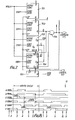
- the peripheral interface 10 includes a controller for the serial link 17 between the CPU part of the system and the keyboard processor 18.
- the controller includes general purpose data latches 701, 702, 703, 704, 705, and a NAND gate 706.
- the data latches 701, 702, 703 and 704 receive data from the CPU 1 or the memory 5 on four data load ports DOH, D1H, D2H, D3H, and provide the data in serial form at the output part of the NAND gate 706 on the line COMDATA which with a second line COMCTL provides the serial link to the keyboard processor 18.
- the data latch 705 receiver data from the keyboard processor via the COMDATA line and the CPU 1 obtains the data from the data register 705.
- the CPU 1 exercises control of the COMDATA line along which the data passes and the keyboard processor 18 supplies clocking pulses along the COMCTL line in order to clock data into and out of the latches as required.
- Fig. 7 Operation of the arrangement represented by Fig. 7 may be better understood by reference to Fig. 8 in which the waveforms labelled A to F represent the voltage variations with time at the correspondingly labelled points in Fig. 7 and the numbers 1 to 11 represent times at which the following conditions are in force:-
- the row addresses of the memory may be arranged differently on the time diagram relating them to the display provided that all rows are addressed within the refresh time for the memory.
- the number of columns addressed during each row address operation may be different from four as described above. It will be appreciated that such changes will affect the arrangement of the connections of the address bus conductors to the multiplexer necessary to enable the memory addresses associated with given positions on the display to be accessed by the use of the coordinates of those positions.
- the protocol of the 2-wire serial link to the keyboard processor may be modified, for exanple, by changing the codes employed or altering the sequence of operations. Modifications may be incorporated in the display to suit different television standards or to give different numbers of picture elements per line. Moreover, the number of bits allocated to each picture element may be different from those given.
Landscapes
- Engineering & Computer Science (AREA)
- Theoretical Computer Science (AREA)
- Physics & Mathematics (AREA)
- General Physics & Mathematics (AREA)
- Computer Hardware Design (AREA)
- General Engineering & Computer Science (AREA)
- Controls And Circuits For Display Device (AREA)
- Processing Of Color Television Signals (AREA)
- Digital Computer Display Output (AREA)
Applications Claiming Priority (2)
| Application Number | Priority Date | Filing Date | Title |
|---|---|---|---|
| GB8400783 | 1984-01-12 | ||
| GB08400783A GB2152711A (en) | 1984-01-12 | 1984-01-12 | A digital computer |
Publications (1)
| Publication Number | Publication Date |
|---|---|
| EP0149511A2 true EP0149511A2 (fr) | 1985-07-24 |
Family
ID=10554882
Family Applications (1)
| Application Number | Title | Priority Date | Filing Date |
|---|---|---|---|
| EP85300029A Withdrawn EP0149511A2 (fr) | 1984-01-12 | 1985-01-03 | Circuit de mémoire pour un dispositif d'affichage |
Country Status (8)
| Country | Link |
|---|---|
| EP (1) | EP0149511A2 (fr) |
| JP (1) | JPS60159932A (fr) |
| KR (1) | KR850005638A (fr) |
| AU (1) | AU3751585A (fr) |
| BR (1) | BR8500134A (fr) |
| ES (1) | ES8602286A1 (fr) |
| GB (1) | GB2152711A (fr) |
| ZA (1) | ZA8410066B (fr) |
Cited By (1)
| Publication number | Priority date | Publication date | Assignee | Title |
|---|---|---|---|---|
| FR2650090A1 (fr) * | 1989-07-21 | 1991-01-25 | Samsung Electronics Co Ltd | Carte video assurant un fonctionnement en mode de niveau 1 bit et un fonctionnement en mode de niveau 2 bits |
Families Citing this family (1)
| Publication number | Priority date | Publication date | Assignee | Title |
|---|---|---|---|---|
| JPS60211692A (ja) * | 1984-04-06 | 1985-10-24 | Hitachi Ltd | 半導体記憶装置 |
-
1984
- 1984-01-12 GB GB08400783A patent/GB2152711A/en not_active Withdrawn
- 1984-12-27 ZA ZA8410066A patent/ZA8410066B/xx unknown
-
1985
- 1985-01-03 EP EP85300029A patent/EP0149511A2/fr not_active Withdrawn
- 1985-01-08 AU AU37515/85A patent/AU3751585A/en not_active Abandoned
- 1985-01-11 BR BR8500134A patent/BR8500134A/pt unknown
- 1985-01-11 KR KR1019850000132A patent/KR850005638A/ko not_active Withdrawn
- 1985-01-11 ES ES539490A patent/ES8602286A1/es not_active Expired
- 1985-01-11 JP JP60003154A patent/JPS60159932A/ja active Pending
Cited By (1)
| Publication number | Priority date | Publication date | Assignee | Title |
|---|---|---|---|---|
| FR2650090A1 (fr) * | 1989-07-21 | 1991-01-25 | Samsung Electronics Co Ltd | Carte video assurant un fonctionnement en mode de niveau 1 bit et un fonctionnement en mode de niveau 2 bits |
Also Published As
| Publication number | Publication date |
|---|---|
| GB2152711A (en) | 1985-08-07 |
| JPS60159932A (ja) | 1985-08-21 |
| ZA8410066B (en) | 1985-10-30 |
| ES539490A0 (es) | 1985-11-16 |
| ES8602286A1 (es) | 1985-11-16 |
| GB8400783D0 (en) | 1984-02-15 |
| KR850005638A (ko) | 1985-08-28 |
| AU3751585A (en) | 1985-07-18 |
| BR8500134A (pt) | 1985-08-20 |
Similar Documents
| Publication | Publication Date | Title |
|---|---|---|
| US5129059A (en) | Graphics processor with staggered memory timing | |
| US4562435A (en) | Video display system using serial/parallel access memories | |
| US4704697A (en) | Multiple station video memory | |
| US4745485A (en) | Picture display device | |
| US5473342A (en) | Method and apparatus for on-the-fly multiple display mode switching in high-resolution bitmapped graphics system | |
| US4682161A (en) | Variable size character display without loss of obscured character positions | |
| US4139838A (en) | Color pattern and alphanumeric character generator for use with raster-scan display devices | |
| US5479184A (en) | Videotex terminal system using CRT display and binary-type LCD display | |
| US4574277A (en) | Selective page disable for a video display | |
| US4581721A (en) | Memory apparatus with random and sequential addressing | |
| EP0201210A2 (fr) | Système d'affichage vidéo | |
| US4620186A (en) | Multi-bit write feature for video RAM | |
| US5546137A (en) | Apparatus and method of transferring video data of a moving picture | |
| WO1981003234A1 (fr) | Appareil d'affichage et de stockage d'informations d'images de television en utilisant une memoire accessible par un ordinateur | |
| US4956708A (en) | Frame memory control system | |
| GB2223650A (en) | Teletext decoder prevents over-writing of special character codes | |
| US5384581A (en) | Image processing apparatus | |
| GB2152711A (en) | A digital computer | |
| JPS6073575A (ja) | デ−タ表示装置 | |
| EP0107687B1 (fr) | Affichage pour un ordinateur | |
| JPH0736162B2 (ja) | 図形処理装置 | |
| JPH0530279B2 (fr) | ||
| EP0283579B1 (fr) | Système d'affichage à balayage à trame avec un générateur de caractères à mémoire à accès direct | |
| US4870407A (en) | Video display apparatus | |
| US4647923A (en) | True object generation system and method for a video display generator |
Legal Events
| Date | Code | Title | Description |
|---|---|---|---|
| PUAI | Public reference made under article 153(3) epc to a published international application that has entered the european phase |
Free format text: ORIGINAL CODE: 0009012 |
|
| AK | Designated contracting states |
Designated state(s): AT BE CH DE FR IT LI LU NL SE |
|
| RAP1 | Party data changed (applicant data changed or rights of an application transferred) |
Owner name: AMSTRAD CONSUMER ELECTRONICS PLC |
|
| STAA | Information on the status of an ep patent application or granted ep patent |
Free format text: STATUS: THE APPLICATION IS DEEMED TO BE WITHDRAWN |
|
| 18D | Application deemed to be withdrawn |
Effective date: 19870803 |
|
| RIN1 | Information on inventor provided before grant (corrected) |
Inventor name: KARLIN, DAVID |