EP0149819A2 - Senseur de rayonnement et système de mesure comportant un tel senseur exposé au rayonnement ainsi qu'un senseur de référence abrité - Google Patents
Senseur de rayonnement et système de mesure comportant un tel senseur exposé au rayonnement ainsi qu'un senseur de référence abrité Download PDFInfo
- Publication number
- EP0149819A2 EP0149819A2 EP84115783A EP84115783A EP0149819A2 EP 0149819 A2 EP0149819 A2 EP 0149819A2 EP 84115783 A EP84115783 A EP 84115783A EP 84115783 A EP84115783 A EP 84115783A EP 0149819 A2 EP0149819 A2 EP 0149819A2
- Authority
- EP
- European Patent Office
- Prior art keywords
- measuring device
- heat
- measuring
- layer
- resistance
- Prior art date
- Legal status (The legal status is an assumption and is not a legal conclusion. Google has not performed a legal analysis and makes no representation as to the accuracy of the status listed.)
- Granted
Links
Images


Classifications
-
- G—PHYSICS
- G01—MEASURING; TESTING
- G01J—MEASUREMENT OF INTENSITY, VELOCITY, SPECTRAL CONTENT, POLARISATION, PHASE OR PULSE CHARACTERISTICS OF INFRARED, VISIBLE OR ULTRAVIOLET LIGHT; COLORIMETRY; RADIATION PYROMETRY
- G01J5/00—Radiation pyrometry, e.g. infrared or optical thermometry
- G01J5/10—Radiation pyrometry, e.g. infrared or optical thermometry using electric radiation detectors
- G01J5/20—Radiation pyrometry, e.g. infrared or optical thermometry using electric radiation detectors using resistors, thermistors or semiconductors sensitive to radiation, e.g. photoconductive devices
- G01J2005/202—Arrays
-
- G—PHYSICS
- G01—MEASURING; TESTING
- G01J—MEASUREMENT OF INTENSITY, VELOCITY, SPECTRAL CONTENT, POLARISATION, PHASE OR PULSE CHARACTERISTICS OF INFRARED, VISIBLE OR ULTRAVIOLET LIGHT; COLORIMETRY; RADIATION PYROMETRY
- G01J5/00—Radiation pyrometry, e.g. infrared or optical thermometry
- G01J5/10—Radiation pyrometry, e.g. infrared or optical thermometry using electric radiation detectors
- G01J5/20—Radiation pyrometry, e.g. infrared or optical thermometry using electric radiation detectors using resistors, thermistors or semiconductors sensitive to radiation, e.g. photoconductive devices
- G01J2005/206—Radiation pyrometry, e.g. infrared or optical thermometry using electric radiation detectors using resistors, thermistors or semiconductors sensitive to radiation, e.g. photoconductive devices on foils
Definitions
- the invention relates to a radiation measuring device (bolometer) and is further directed to a measuring system which is constructed using the same and consists of a measuring device which is exposed to the radiation and a reference device shielded against the radiation.
- the spectral range to be measured extends from the infrared range to the range of soft X-rays in the 10 keV range.
- bolometers For broadband radiation measurements, radiation measuring devices called bolometers are used. This is radiation detectors that are sensitive to a wide spectral range (infrared to soft X-rays). They measure the incident radiation power integrally. The action of the bolometer is based on the absorption of the radiation to be measured and the resulting heating of the bolometer detector. The bolometer signal is proportional to the temperature rise of the detector and the sensitivity depends on the temperature coefficient of the physical effect used to measure the temperature rise.
- the radiation power emitted on the plasma and incident on the detector is of the order of a few mW. In order to be able to measure this low radiation power, the use of foil bolometers is recommended.
- Sensitivity of signal transmission to low-frequency interference If high-frequency heaters are used for the plasma experiment, large interference is to be expected for the bolometer measurements.
- the absorber layer merges into a laterally protruding heat-conducting layer which is in thermally conductive contact with it and in that the heat-conducting layer is shielded from the radiation to be measured.
- the absorber layer and optionally the heat conducting layer can consist of a noble metal, preferably gold. It is expedient if, in a further embodiment of the invention, the heat-conducting layer consists of a layer that projects laterally, significantly thinner, possibly in one piece with it and / or is made of the same material as the absorber layer.
- the solution according to the invention separates the energy absorption and the heat conduction from one another, as a result of which the dimensions of the detector can be significantly reduced, so that in a further embodiment of the invention a plurality of heat-conducting surfaces, each carrying an absorber layer, can be arranged next to one another in a row.
- M on can switch the high-resistance layers assigned to the absorber layers in each case in a separate resistance measuring bridge.
- Another way to measure is that of the high resistance layers associated with the absorber layers at least some connected in series and the resistance groups formed in this way are connected in a separate resistance measuring bridge.
- the resistance value of a measuring system can thus be increased accordingly, as a result of which the bridge voltage can be increased correspondingly with the same power applied to the resistors and the sensitivity of the measuring system can thus be improved.
- the fixed resistor opposite the high-resistance resistor layer in the measuring bridge is also designed as a high-resistance resistor layer and is arranged together with the high-resistance resistor layer on the side of the carrier film facing away from the absorber within a boundary corresponding to the boundary of the absorber layer.
- the heat-conducting layers are connected to one another via a heat sink, the extent of the entire measuring system can be significantly reduced because this prevents the individual detectors from interfering with one another because of the direct dissipation of the heat to the environment via the heat sink.
- the procedure is preferably such that the heat sink is in contact with the heat-conducting layers and is much larger than the thickness dimensions of the absorber and heat-conducting layers and is made of a good heat-conducting material, each of which has a recess in the region of the absorber layers, the lateral boundary of which is a distance from the lateral limits of the Have absorber layers and the respective top surface is provided with a window, the dimensions of which correspond to those of the absorber layer.
- the heat sink can also consist of the material of the heat-conducting layers and be formed in one piece with them.
- a coating is expediently applied to the carrier film, which has recesses, each with a bottom, the central region of which forms the absorber layer, which merges into the material of the coating, which forms the heat sink as a whole, via a thin edge region forming the heat-conducting layer.
- the distance between the delimitation of the respective recess and the delimitation of the respective absorber layer is preferably selected such that the heat transfer between the absorber layer and the high-resistance resistor layer takes place much faster than the heat transfer from the delimitation of the absorber layer into the heat sink.
- the distance between the lateral boundary of the absorber layers and the heat sink is matched to the thickness of the heat conducting layer.
- solderable connection surfaces are provided on the side of the carrier film carrying the high-resistance resistance layers in the arrangement surrounding the resistance layers.
- the construction is expediently chosen so that the structure of the reference device is identical to that of the measuring device and the reference device is arranged in the same housing as the measuring device.
- the measuring device and reference bolometer are preferably arranged one behind the other in the housing.
- solderable connection surfaces are duplicated on the side of the two carrier foils carrying the resistors and can be connected in series, so that inner and outer connection surfaces are created.
- outer solderable pads are then conductively connected to first contact pins in the measuring device and the inner solderable pads are conductively connected to second contact pins in the reference device, while the outer pads are drilled out.
- the first contact pins pass freely through these bores and the ends of the first and second contact pins form the common contact body of the measuring system consisting of the measuring bolometer and the reference bolometer.
- the measuring device is clamped between two heat sinks with the corresponding recesses and provided with mechanically stable connections.
- the heat sinks are aluminum disks that cool the detectors to the housing temperature of the measuring system.
- the heat sink lying on the absorber side is designed so that the heat-conducting surfaces are touched at their edges by the heat sink placed thereon.
- This heat sink has cutouts, each of which in turn has a window that only allows access to the absorber.
- the measuring device can be mounted flat because of the disk-like design of the heat sink.
- the measuring device can be optically adjusted by recesses in the heat sink resting on the resistance side.
- the overall construction is particularly easy to assemble. It is only necessary to punch the through holes through the measuring or reference device for clamping screws and the contact pins.
- the measuring and reference devices can then be assembled and soldered and finally the measuring system can simply be plugged together.
- a threaded ring is sufficient to secure the assembled individual elements.
- the measuring device and the reference device are arranged side by side on the carrier film, whereby of course only the measuring device is exposed to the radiation, but the reference device must be shielded from the radiation to be measured.
- the arrangement of the measuring system in a further embodiment of the invention is such that the high-resistance layers of the measuring device and the high-resistance layers of the reference device are each formed as meanders and the meanders of the high-resistance layers of the measuring device or reference device are interlocked on the carrier film and on opposite sides
- This juxtaposition of measuring and reference device each have two conductor tracks opening out into connecting surfaces, of which the outer ones loop around the inner surfaces of the inner conductor tracks, one meander of one bolometer between the two outer conductor tracks and the other meander of this bolometer between is connected to the inner conductor tracks, while the two meanders of the other bolometer are each connected between an outer and an inner conductor track, enables an embodiment which can be carried out with a single mask without j normal overlap of conductor tracks can be produced.
- meander should of course in be understood to the greatest extent and not only include comb-like structures. Spiral routings can also be nested one inside the other and enable connections at the outer spiral ends if they are designed as double spirals running back and forth. When choosing the meander, one will always proceed in such a way that connections are possible in the level of the meander and not those that are angled to this level.
- the specified arrangement can be provided in a further embodiment of the invention in a preferably symmetrical arrangement on a carrier film.
- Fig. 1, 1 denotes a carrier film made of an electrically insulating material, for example made of mica or from the plastic material known under the trademark "Capton". These materials are particularly suitable because of their high radiation resistance and strength against high temperatures.
- the heat-conducting layer 2 which preferably consists of gold or platinum, is evaporated onto the carrier film 1.
- the thickness of this layer is approximately 0.5 ⁇ m and less.
- an absorber layer 3 is vapor-deposited, which consists of the same material as the heat-conducting layer 2 and has a thickness of approximately 4 ⁇ m. This absorber layer 3 forms the measuring surface. The thickness of the absorber layer 3 can be freely selected depending on the radiation to be measured.
- the layers 2 and 3 can also be integral with one another.
- a high-resistance resistor layer 4 which is formed, for example, in a meandering shape and can likewise consist of evaporated gold or platinum.
- the resistance M formed by the resistance layer 4 2 lies in a branch 5 of a Wheatstone bridge 6, which also has three further resistors 7, 8 and 9, of which the resistor 9 can be the resistance layer R of a reference device.
- a measuring device 10 is connected across the one diagonal of the bridge, while a voltage U is present at the other diagonal. Touching the edges of the heat-conducting layer 2 is a heat sink 11, which extends inwards with projections 12, which form a shield, which only leaves access to the absorber layer 3, which is hit by the schematically indicated radiation F.
- the carrier film 1, together with the heat-conducting layer 2, the absorber layer 3 and the resistance layer 4, forms the detector of the measuring device, which can also be referred to as a film bolometer.
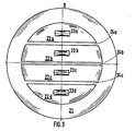
- FIG. 3 shows an arrangement with four detectors lying next to one another in plan view, but without a shielding heat sink.
- the carrier film designated 21 which in the present case is designed as a circular structure.
- four absorber layers, designated 23a, 23b, 23c and 23d, are provided in series, each of which sits on heat-conducting layers 22a, 22b, 22c, 22d.
- the formation of these heat-conducting layers is such that they conform to the circular outline of the carrier film 21 while maintaining the appropriate distances 24a, 24b and 24c.
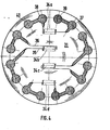
- the bottom view of the carrier film shown in FIG. 4, which is designated here by 31, shows the high-resistance layers 34a, 34b, 34c and 34d. These are located exactly under the absorber layers 23a, 23b, 23c, 23d on the other side of the carrier film, as designated by 21 in FIG. 3, so that there is absorber layer and corresponding high-resistance layer, for example absorber layer 23a and high-resistance layer 34a lie exactly opposite on both sides of the carrier film.
- the high-resistance layers are formed in a meandering shape.
- the individual resistance layers are connected via lines 35, 36, which are provided with reference numerals only for the resistance layer 34b, to inner connection surfaces 37 and 38 which are connected to further outer connection surfaces 39 and 40.
- Such a structure as can be seen from FIGS. 3 and 4 in detail, is not only provided for the measuring device exposed to the radiation, but also for a reference device provided in the measuring system which is not exposed to radiation, but rather is shielded against the radiation to be measured .
- the measuring device exposed to the radiation and the reference device shielded against the radiation are arranged one behind the other in a single housing.
- the resistance layer (s) of the reference device are electrically connected into the Wheatstone bridge 6 according to FIG. 2 and correspond there to the resistor 9.
- FIG. 5 shows the heat sink 41 to be placed on the carrier film with applied heat layers and absorber layers, which has the recesses 42a, 42b, 42c and 42d, which have windows 43a, 43b, 43c and 43d on their top surface.
- the arrangement is clearer from the sectional view according to FIG. 6.
- the heat sink 51 can be seen there with the recesses 53a, 53b, 53c and 53d, in the top surfaces 54a, 54b, 54c and 54d of which windows 55a, 55b, 55c and 55d are provided whose dimensions, like the drawing. 3 clearly shows the dimensions of the absorber layers 23a, 23b, 23c and 23d.
- FIG. 7 shows an exploded perspective view of an embodiment of a measuring system with the measuring device according to the invention and a reference device.
- a cylindrical housing 71 is provided with an inner collar 72 at one end.
- the arrangement designated 73 is supported on this inner collar 72 when it is inserted into the cylindrical housing 71 from the right according to FIG. 7.
- the fixation takes place with the aid of a threaded ring 74, which is screwed into a corresponding internal thread on the other, here right end of the cylindrical housing 71.
- the heat sink just described in connection with FIGS. 5 and 6 is designated by 75 and thus has the corresponding wall thickness and the corresponding recesses and the corresponding windows.
- 76 means the representation of the measuring device exposed to the radiation, consisting of carrier foil and heat conducting layers and absorber layers placed in the direction of the radiation (arrows F).
- a base 77 which consists of an insulating material and is inserted in the contact pins 78, then follows.
- the contact pins 78 protrude through the base 77 and end on the side facing the measuring device 76 in contact areas which can be easily connected to the contact areas on the measuring device 76.
- the underside of the carrier film ie the side carrying the resistance layers, is in contact with a heat sink, namely a cylindrical body made of aluminum, which, however, has recesses such that it does not short-circuit the individual connections and resistance layers.
- a heat sink namely a cylindrical body made of aluminum, which, however, has recesses such that it does not short-circuit the individual connections and resistance layers.
- This heat sink is in the drawing designated with the reference number 79.
- a continuous separating disk 80 then follows, for example an aluminum disk, which completely shields the measuring part of the system (measuring device) against the reference part (reference device).
- a heat sink is designated, which corresponds to the cooling body 75 in all respects.
- a reference device which corresponds to the measuring device 76 in all respects.
- a base 83 which essentially corresponds to the base 77 and carries contact pins 84 corresponding to the contact pins 78.
- These contact pins 84 are offset from the contact pins 78 so that they sit exactly in the middle between the contact pins 78.
- a heat sink is provided which essentially corresponds to the cooler 79.
- Both types of contact pins 78 and 84 are plugged into a common base 86, which is an insulating body similar to the bases 77 and 83.
- connection areas are drilled out on the side of the carrier film carrying the resistance layers, through which the contact pins 78 reach, so that no contact is made between the reference bolometer and the actual measuring bolometer exposed to the radiation, but rather the corresponding row of contacts via the base 83 protrudes and is expediently inserted into an end socket carrying a corresponding number of contacts.
- the measuring and reference device By arranging the measuring and reference device in such a way that the contacts are offset from one another, and by connecting them to a Wheatstone bridge, a compensation of temporally different magnetic fields is achieved. You can achieve this by installing the reference device moreover, a complete compensation of immeasurable radiation parts, which only heat the housing and the parts of the measuring system connected to it, without influencing the measurement.
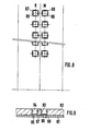
- the measuring and reference device are arranged side by side and several such device pairs are arranged one behind the other in a row.
- the measuring devices In the right row M the measuring devices should sit in the left row R the reference devices.
- Fig. 9 the structure is indicated in section. 91 means the carrier film, onto which a gold layer 92 is evaporated, which form the heat sink. She has z. B. a thickness of 25 ⁇ m. In this layer 92 recesses 93 and 94 are formed, which have a bottom, the central region 95 and 96 each having an absorber layer of z. B. 4 ⁇ m thickness that directly over an edge region 9 or 98 (vlg. Also Fig. 8), which has a correspondingly smaller thickness of z. B. has only 0.5 microns and forms the heat-conducting layer, merges into the heat sink layer 92. The absorber layer, the heat-conducting layer and the heat sink are therefore in one piece. The production of such a structure in the vapor deposition and etching process presents no difficulties.
- the heat-conducting layer and the heat sink are covered by a cover made of a suitable material and restricting the radiation only to the absorber layer of the measuring device by means of windows.
- the absorber layer is of course also shielded from the incident radiation by this cover.
- the cover is not shown in Fig. 9.
- the windows restricting the radiation onto the desired absorber layers can also be realized by cantilevered edges on the corresponding recesses 93, but this configuration is difficult and also complex.
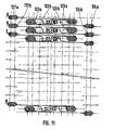
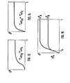
- FIG. 10 shows a pair of high-resistance layers belonging to a pair of measuring and reference devices, which is provided on the side facing away from the measuring and reference device side, measuring and reference devices precisely adapted in their position.
- the arrangements 101 and 102 include not only those belonging to the respective measuring resistor M (cf. resistor 4 according to FIG. 2) or to the respective reference resistor R (cf. resistor 9 according to FIG. 2), here each in the form of a flat meander Resistance winding, but also the winding in the measuring bridge opposite each other, which is also formed as a meander (cf. resistor 8 or 7 according to FIG. 2).
- meanders can, as can be seen in FIG.
- a connecting line leads to a conductor track 104, which is guided around a connection surface 105 and then as the one outer conductor path 106 to the outer connection surface 107.
- a connection line 108 leads from the structure 102 to a conductor track 109, which leads around a connection area 110 and then as the other outer conductor track 111 to the other outer connection area 112.
- the one end on the connecting line 103 The resistance of the structure 101 lies at the other end on the outer conductor 111.
- the resistance of the structure 102 with one end on the connecting line 108 lies at the other end both on an inner conductor 113 leading to the connection surface 110 and on a connecting part 114, which is also connected to the second resistor in the structure 101, which is connected at its other end to the conductor track 115, which leads to the inner connection surface 105.
- one end of the second resistor 102 is connected to the conductor track 115, and its other end lies on the outer conductor track 106.
- FIG. 11 shows the multiple arrangement of such circuits shown in detail in FIG. 10. So that adjacent circuits A, B, C ... N do not mutually interfere with one another, the connection areas 121a and 122a of the circuit A are connected to the AC voltage supply of the bridge circuit, while the connection of the remaining two connection areas 123a and 124a forms the measurement diagonal. In the next circuit B, the connections are reversed, ie the measurement diagonal is between the connection areas 121b and 122b, while the supply diagonal is between the connection areas 123b and 124b. In circuit C, the connection conditions are again like in the circuit A, etc.
- the absorber layer is exposed to the radiation to be measured.
- the radiation absorbed in the absorber layer leads to heating of the absorber layer.
- the heat flows in the direction of the high-resistance layer and towards the sides.
- the resistance layer changes its resistance value measurably, and the clearer the higher the resistance it is.
- the incident radiation leads to a further heating of the absorber layer until the heat flowing off to the sides is equal to the absorbed radiation power.
- the heat is from the massive heat sink with great. heat capacity and negligible heating removed.
- the change in the resistance of the resistance layer on the side of the carrier film opposite the absorber layer is a measure of the temperature change averaged over the area of the resistance or absorber layer. It can be shown that the temperature change of the detector in response to a step function of the power can be approximately represented by an exponential function of the following form:
- the constants ⁇ eff and c eff are called the bolometer constant.
- the bolometer detector It is therefore important to constructively design the bolometer detector so that the heat flow from the absorber side through the thin carrier film to the resistance layer takes place in a considerably shorter time than the lateral outflow of the heat from the absorber layer to which it is applied limiting heat sink. It is essential that the measuring bolometer facing the radiation source is completely covered with an electrically conductive and heat-conducting layer in order to avoid charging by secondary electrons and to achieve defined heat transport conditions to the heat sink as well as defined characteristic data.
- the outflow of heat can be influenced constructively by increasing or decreasing the thickness of the absorber layer, but also by increasing or decreasing its length or width dimensions.
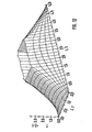
- the temperature difference ⁇ o of the absorber layer for the detector with a large time constant (B) and that with a small time constant (A) is almost identical, while for long times t the temperature change ⁇ A is less than for the case ( B).
- the higher sensitivity can therefore only be used for longer times, but it is sufficient that the signal-to-noise ratio is approximately 1000.
- a further increase in the time constant leads to a restriction of the dynamics compared to the radiation outputs to be measured and the self-radiation of the absorbers layer is no longer negligible due to the higher detector temperature.
Landscapes
- Physics & Mathematics (AREA)
- General Physics & Mathematics (AREA)
- Spectroscopy & Molecular Physics (AREA)
- Radiation Pyrometers (AREA)
- Photometry And Measurement Of Optical Pulse Characteristics (AREA)
- Measurement Of Radiation (AREA)
Applications Claiming Priority (4)
| Application Number | Priority Date | Filing Date | Title |
|---|---|---|---|
| DE3401946 | 1984-01-20 | ||
| DE3401946 | 1984-01-20 | ||
| DE3408724A DE3408724A1 (de) | 1984-01-20 | 1984-03-09 | Strahlungsmessgeraet und unter verwendung desselben ausgebildetes, aus einem der strahlung ausgesetzten messgeraet und einem gegen die strahlung abgeschirmten referenzgeraet bestehenden messsystem |
| DE3408724 | 1984-03-09 |
Publications (3)
| Publication Number | Publication Date |
|---|---|
| EP0149819A2 true EP0149819A2 (fr) | 1985-07-31 |
| EP0149819A3 EP0149819A3 (en) | 1986-07-16 |
| EP0149819B1 EP0149819B1 (fr) | 1989-07-19 |
Family
ID=25817750
Family Applications (1)
| Application Number | Title | Priority Date | Filing Date |
|---|---|---|---|
| EP84115783A Expired EP0149819B1 (fr) | 1984-01-20 | 1984-12-19 | Senseur de rayonnement et système de mesure comportant un tel senseur exposé au rayonnement ainsi qu'un senseur de référence abrité |
Country Status (4)
| Country | Link |
|---|---|
| US (1) | US4687342A (fr) |
| EP (1) | EP0149819B1 (fr) |
| JP (1) | JP2622539B2 (fr) |
| DE (2) | DE3408724A1 (fr) |
Families Citing this family (15)
| Publication number | Priority date | Publication date | Assignee | Title |
|---|---|---|---|---|
| JPS6275369A (ja) * | 1985-09-30 | 1987-04-07 | Toshiba Corp | 放射線検出装置 |
| US4904869A (en) * | 1988-12-14 | 1990-02-27 | Progress Technologies Corporation | X-ray sensor having a high mass number convertor and a superconducting detector |
| DE3927735A1 (de) * | 1989-08-23 | 1991-02-28 | Asea Brown Boveri | Strahlungsthermometer |
| US5634718A (en) * | 1994-07-27 | 1997-06-03 | The United States Of America As Represented By The Secretary Of Commerce | Particle calorimeter with normal metal base layer |
| DE19527226A1 (de) * | 1995-07-26 | 1997-01-30 | Applied Precision S R O | Thermoelektrischer Meßkonverter |
| EP0794415A1 (fr) * | 1996-03-06 | 1997-09-10 | Koninklijke Philips Electronics N.V. | Dispositif de mesure de température sans contact |
| DE19808132B4 (de) * | 1997-02-27 | 2009-10-29 | Ust Umweltsensortechnik Gmbh | Bauelement zum Senden und Empfangen von infraroter Strahlung |
| RU2194955C2 (ru) * | 1998-05-21 | 2002-12-20 | Открытое акционерное общество "ЛОМО" | Устройство для обнаружения и преобразования мощности источника излучения (варианты) |
| ITMI20012475A1 (it) * | 2001-11-23 | 2003-05-23 | Luigi Argenti | Strumento per la misura della potenza della radiazione emessa da una sorgente laser nonche' procedimento attuato per la misura della potenza |
| US7125163B2 (en) * | 2003-11-24 | 2006-10-24 | The Boeing Company | Simple high accuracy high energy calorimeter |
| ITMI20051090A1 (it) * | 2005-06-13 | 2006-12-14 | Laser Point S R L | "dispositivo atto a rilevare ottici di un fascio laser" |
| WO2008127648A1 (fr) * | 2007-04-13 | 2008-10-23 | Ion Optics, Llc | Appareil et procédé de spectroscopie par absorption |
| US9933312B2 (en) * | 2016-09-08 | 2018-04-03 | Robert Bosch Gmbh | Bolometer fluid flow and temperature sensor |
| JP7030640B2 (ja) * | 2018-07-26 | 2022-03-07 | 株式会社東芝 | 放射線検出器および放射線検出装置 |
| KR20220133214A (ko) * | 2020-02-06 | 2022-10-04 | 트리나미엑스 게엠베하 | 차동 이중 검출기를 통한 온도 검출 |
Family Cites Families (12)
| Publication number | Priority date | Publication date | Assignee | Title |
|---|---|---|---|---|
| DE106082C (fr) * | ||||
| DE61359C (de) * | TH. PH. CH. CRAMPTON in London, 10 Cursitor Street, Chancery Lane, und A. ESSINGER in Frankfurt a. M., Eckenheimer Landstr. 20; Ver_ treter: F. C. GLASER, Königl. Geh. Kommission^, rath, in Berlin S.W., Lindenstrafse 80. Vom 5. Ju!j 1890 ab | Kohlenhalter für Bogenlampen | ||
| US2986034A (en) * | 1957-10-18 | 1961-05-30 | Robert C Jones | Air-backed thermistor bolometer |
| US3229235A (en) * | 1960-05-02 | 1966-01-11 | Hughes Aircraft Co | Thermal radiant energy detecting device |
| US3535523A (en) * | 1967-02-01 | 1970-10-20 | Hewlett Packard Co | Radiant flux measuring apparatus of the thermopile type |
| US3693011A (en) * | 1971-02-02 | 1972-09-19 | Hughes Aircraft Co | Ion implanted bolometer |
| DD106082A1 (fr) * | 1973-06-27 | 1974-05-20 | ||
| US3939706A (en) * | 1974-04-10 | 1976-02-24 | The Boeing Company | High energy sensor |
| US4001586A (en) * | 1975-05-09 | 1977-01-04 | Plessey Incorporated | Thick film sensor and infrared detector |
| US4061917A (en) * | 1976-05-24 | 1977-12-06 | Goranson Rex W | Bolometer |
| US4063095A (en) * | 1976-12-10 | 1977-12-13 | Solomon Wieder | Balancing radiometer |
| JPS57172784A (en) * | 1981-04-17 | 1982-10-23 | Univ Kyoto | Thermoelectric conversion element |
-
1984
- 1984-03-09 DE DE3408724A patent/DE3408724A1/de active Granted
- 1984-12-19 DE DE8484115783T patent/DE3479051D1/de not_active Expired
- 1984-12-19 EP EP84115783A patent/EP0149819B1/fr not_active Expired
-
1985
- 1985-01-18 JP JP60007331A patent/JP2622539B2/ja not_active Expired - Lifetime
- 1985-01-18 US US06/692,843 patent/US4687342A/en not_active Expired - Lifetime
Non-Patent Citations (4)
| Title |
|---|
| ANALYTICAL CHEMISTRY, Band 51, Nr. 6, Mai 1979, Seiten 712-717; D.G. TAYLOR et al.: "Light entensity measurements I: large area bolometers with microwatt sensitivities and absolute calibration of the Rhodamine B quantum counter" * |
| MESSEN UND PR]FEN, Nr. 3, März 1982, Seiten 164-167, Bad Wörlshofen, DE; "Dünne Schichten für Messgrössenwandler" * |
| REVIEW OF SCIENTIFIC INSTRUMENTS, Band 53, Nr. 10, Oktober 1982, Seiten 1527-1534, New York, US; J. SCHIVELL et al.: "Bolometer for measurements on high-temperature" * |
| TECHNISCHES MESSEN, Band 49, Nr. 10, Oktober 1982, Seiten 355-357, M}nchen, DE; R. HARTMANN et al.: "Hochempfindliche Bolometer in D}nnschichttechnik" * |
Also Published As
| Publication number | Publication date |
|---|---|
| US4687342A (en) | 1987-08-18 |
| EP0149819B1 (fr) | 1989-07-19 |
| DE3408724A1 (de) | 1985-07-25 |
| JP2622539B2 (ja) | 1997-06-18 |
| DE3479051D1 (en) | 1989-08-24 |
| DE3408724C2 (fr) | 1988-10-27 |
| EP0149819A3 (en) | 1986-07-16 |
| JPS60161580A (ja) | 1985-08-23 |
Similar Documents
| Publication | Publication Date | Title |
|---|---|---|
| EP0149819B1 (fr) | Senseur de rayonnement et système de mesure comportant un tel senseur exposé au rayonnement ainsi qu'un senseur de référence abrité | |
| DE2806858C2 (fr) | ||
| DE4300605C2 (de) | Sensorchip | |
| DE4436876A1 (de) | Sensorchip | |
| DE2017067B2 (de) | Pyroelektrischer Detektor | |
| WO2003062854A2 (fr) | Detecteur concu pour detecter des faisceaux de particules et procede de fabrication dudit detecteur | |
| DE2948742C2 (fr) | ||
| DE2949862A1 (de) | Festkoerperstrahlungsdetektor und anordnungen derselben | |
| DE3438764A1 (de) | Thermoelektrischer detektor | |
| EP0030056B1 (fr) | Dispositif de sonde à influence et procédé pour sa fabrication | |
| EP3546931B1 (fr) | Capteur de gaz thermorésistif, detecteur d'écoulement et capteur de conductivité thermique | |
| EP0629862A1 (fr) | Dispositif de mesure d'un écoulement radial d'un gaz ou d'un liquide avec un pont de wheatstone comprenant quatre résistances dépendant de la température | |
| EP0584866B1 (fr) | Magnétomètre à Squid avec une enveloppe de blindage contre des champs électromagnétiques parasites | |
| DE69216862T2 (de) | Verwendung von vanadium oxyd in mikrobolometer sensoren | |
| DE19711874C2 (de) | Folienmanometer | |
| EP0123062A1 (fr) | Diviseur de courant pour transformateur de mesure destiné à la mesure d'un courant | |
| DE3142949C2 (fr) | ||
| WO1998043058A9 (fr) | Manometre a feuille | |
| EP0513557A2 (fr) | Dispositif supraconducteur à effet tunnel | |
| DE2243979C3 (de) | Magnetoresistive Abfühlanordnung mit Rauschunterdrückung | |
| DE2923799C2 (de) | Diffundierter Halbleiterwiderstand | |
| DE4208135A1 (de) | Vorrichtung zur messung einer gas- oder fluessigkeitsstroemung | |
| DE69531266T2 (de) | Magnetsensor | |
| DE102021132701A1 (de) | Vorrichtung zur steuerung von gefangenen ionen mit einem temperatursensor | |
| DE102014011670B3 (de) | Magnetfeldfluktuationsthermometer |
Legal Events
| Date | Code | Title | Description |
|---|---|---|---|
| PUAI | Public reference made under article 153(3) epc to a published international application that has entered the european phase |
Free format text: ORIGINAL CODE: 0009012 |
|
| AK | Designated contracting states |
Designated state(s): CH DE FR GB IT LI SE |
|
| RIN1 | Information on inventor provided before grant (corrected) |
Inventor name: MUELLER, REINHOLD, DR. Inventor name: MAST, KARL-FRIEDRICH, DR.-PHYS. Inventor name: BETZLER, PETER, DIPL.-ING. |
|
| PUAL | Search report despatched |
Free format text: ORIGINAL CODE: 0009013 |
|
| AK | Designated contracting states |
Kind code of ref document: A3 Designated state(s): CH DE FR GB IT LI SE |
|
| 17P | Request for examination filed |
Effective date: 19860812 |
|
| 17Q | First examination report despatched |
Effective date: 19880321 |
|
| GRAA | (expected) grant |
Free format text: ORIGINAL CODE: 0009210 |
|
| AK | Designated contracting states |
Kind code of ref document: B1 Designated state(s): CH DE FR GB IT LI SE |
|
| REF | Corresponds to: |
Ref document number: 3479051 Country of ref document: DE Date of ref document: 19890824 |
|
| ITF | It: translation for a ep patent filed | ||
| GBT | Gb: translation of ep patent filed (gb section 77(6)(a)/1977) | ||
| ET | Fr: translation filed | ||
| PLBE | No opposition filed within time limit |
Free format text: ORIGINAL CODE: 0009261 |
|
| STAA | Information on the status of an ep patent application or granted ep patent |
Free format text: STATUS: NO OPPOSITION FILED WITHIN TIME LIMIT |
|
| 26N | No opposition filed | ||
| ITTA | It: last paid annual fee | ||
| EAL | Se: european patent in force in sweden |
Ref document number: 84115783.7 |
|
| PGFP | Annual fee paid to national office [announced via postgrant information from national office to epo] |
Ref country code: CH Payment date: 19991125 Year of fee payment: 16 |
|
| PGFP | Annual fee paid to national office [announced via postgrant information from national office to epo] |
Ref country code: SE Payment date: 19991126 Year of fee payment: 16 |
|
| PG25 | Lapsed in a contracting state [announced via postgrant information from national office to epo] |
Ref country code: SE Free format text: LAPSE BECAUSE OF NON-PAYMENT OF DUE FEES Effective date: 20001220 |
|
| PG25 | Lapsed in a contracting state [announced via postgrant information from national office to epo] |
Ref country code: LI Free format text: LAPSE BECAUSE OF NON-PAYMENT OF DUE FEES Effective date: 20001231 Ref country code: CH Free format text: LAPSE BECAUSE OF NON-PAYMENT OF DUE FEES Effective date: 20001231 |
|
| EUG | Se: european patent has lapsed |
Ref document number: 84115783.7 |
|
| REG | Reference to a national code |
Ref country code: CH Ref legal event code: PL |
|
| REG | Reference to a national code |
Ref country code: GB Ref legal event code: IF02 |
|
| PGFP | Annual fee paid to national office [announced via postgrant information from national office to epo] |
Ref country code: FR Payment date: 20031128 Year of fee payment: 20 |
|
| PGFP | Annual fee paid to national office [announced via postgrant information from national office to epo] |
Ref country code: GB Payment date: 20031217 Year of fee payment: 20 |
|
| PGFP | Annual fee paid to national office [announced via postgrant information from national office to epo] |
Ref country code: DE Payment date: 20040223 Year of fee payment: 20 |
|
| PG25 | Lapsed in a contracting state [announced via postgrant information from national office to epo] |
Ref country code: GB Free format text: LAPSE BECAUSE OF EXPIRATION OF PROTECTION Effective date: 20041218 |
|
| REG | Reference to a national code |
Ref country code: GB Ref legal event code: PE20 |