EP0150076A2 - Parallel-Serien-Umsetzer - Google Patents
Parallel-Serien-Umsetzer Download PDFInfo
- Publication number
- EP0150076A2 EP0150076A2 EP85200009A EP85200009A EP0150076A2 EP 0150076 A2 EP0150076 A2 EP 0150076A2 EP 85200009 A EP85200009 A EP 85200009A EP 85200009 A EP85200009 A EP 85200009A EP 0150076 A2 EP0150076 A2 EP 0150076A2
- Authority
- EP
- European Patent Office
- Prior art keywords
- parallel
- transmission line
- inputs
- series
- series converter
- Prior art date
- Legal status (The legal status is an assumption and is not a legal conclusion. Google has not performed a legal analysis and makes no representation as to the accuracy of the status listed.)
- Granted
Links
Images

Classifications
-
- H—ELECTRICITY
- H03—ELECTRONIC CIRCUITRY
- H03K—PULSE TECHNIQUE
- H03K5/00—Manipulating of pulses not covered by one of the other main groups of this subclass
- H03K5/01—Shaping pulses
- H03K5/04—Shaping pulses by increasing duration; by decreasing duration
- H03K5/06—Shaping pulses by increasing duration; by decreasing duration by the use of delay lines or other analogue delay elements
-
- H—ELECTRICITY
- H03—ELECTRONIC CIRCUITRY
- H03K—PULSE TECHNIQUE
- H03K5/00—Manipulating of pulses not covered by one of the other main groups of this subclass
- H03K5/01—Shaping pulses
- H03K5/12—Shaping pulses by steepening leading or trailing edges
-
- H—ELECTRICITY
- H03—ELECTRONIC CIRCUITRY
- H03M—CODING; DECODING; CODE CONVERSION IN GENERAL
- H03M9/00—Parallel/series conversion or vice versa
Definitions
- the invention relates to a parallel-series converter having a plurality of parallel inputs and comprising a combining arrangement having a plurality of inputs equal in number to the plurality of parallel inputs of the parallel-series converter, and a series output.
- the invention has for its object to provide a solution to the above problem and is characterized in that each parallel input is connected via the series arrangement of a terminating impedance and a transmission line to a respective one of the inputs of the combining arrangement, the time delays of the individual transmission lines having respective different magnitudes according to an arithmetical progression, the junction between each terminating impedance and the associated transmission line being connected to a short-circuited transmission line having a length A/2, where ⁇ is the wavelength of the desired output frequency of the parallel-series converter, each original pulse as applied to the input of the relevant short-circuited transmission line appearing again after a short period of time with a delay and in inverted form at the same input, such that the original pulse, during the time it is overlapped by the' inverted pulse, is wholly or substantially wholly, eliminated.
- a parallel-series converter In a parallel-series converter according to the invention, use is made predominantly of passive elements to effect the parallel-series conversion. As a result, the additional dissipation due to the parallel-series converter and added to the total dissipation is drastically reduced.
- the parallel inputs are constituted by the terminals 31, 32 and 33 and the information is applied to these terminals by sources 1, 2 and 3.
- the input 31 is connected to a first input 41 of a combining arrangement I via the series arrangement of a terminating impedance 4 and a transmission line 7.
- the input 32 is connected to a second input 42 of the combining arrangement I via the series arrangement of a terminating impedance 5 and a transmission line 8.
- the input 33 is connected to a third input 43 of the combining arrangement I via the series arrangement of a terminating impedance 6 and a transmission line 9.
- the input 41 is connected to a terminating impedance 13 and also to the base electrode of a transistor 17.
- the input 42 is connected to a terminating impedance 14 and also to the base electrode of a transistor 18.
- the input :43 is connected to a terminating impedance 15 and also to the base electrode of a transistor 19.
- the collectors of the transistors 17, 18 and 19 are connected to the positive pole (+) of a supply voltage and also via a resistor 21 to an output 23 of the parallel-series converter.
- the collector of a transistor 20 is connected to the output 23 of the parallel-series converter.
- the emitters of the transistors 17, 18, 29 and 20 are connected in common to a point 24 of constant potential via a resistor 22.
- the base electrode of the transistor 20 is connected to a source of reference voltage 16.
- the junction point of the terminating impedance 4 and the transmission line 7 is connected to a short-circuited transmission line 10.
- the junction of the terminating impedance 5 and the transmission line 8 is connected to a short-circuited transmission line 11.
- the junction of the terminating impedance 6 and the transmission line 9 is connected to a short-circuited transmission line 12.
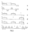
- a digital signal which is of the shape shown in Fig. 2a, is applied to the inputs of the parallel-series converter.
- the widths of the pulses applied to the inputs are limited, such as described, for example, in United States Patent 3,515,995. This is necessary as otherwise loss of information would occur in the parallel-series converter.
- negative reflection pulses are produced at the input of the short-circuited transmission line, as shown in Fig. 2b. These reflection pulses are unwanted and are suppressed in the combining arrangement I with the aid of the transistor 20 and the reference voltage 16 source. Mutatis mutandis it is alternatively possible to utilize the negative pulse and to eliminate the positive pulse.
- a further method of suppressing the unwanted reflection pulses is, for example, to provide a diode between the short-circuited transmission line 10 and the transmission line 7. This diode is arranged such that only the positive pulses are allowed to pass to the transmission line-7.
- Fig. 2c shows by way of example a voltage variation of the pulses produced by the source 1.
- Fig . 2d shows by way of example a voltage variation of pulses produced by the source 2 and
- Fig. 2e shows the voltage variation of the pulses produced by source 3.
- the three parallel bit streams (1, 1, 1), (1, 0, 1) and (0, 1, 1) appear in this succession at the inputs 31, 32 and 33. Due to the action of the respective short-circuited transmission lines 10, 11 and 12, the pulse widths of the pulses from these parallel bit streams are limited as is shown in Fig. 2b.
- the three parallel bit streams of three bits each are thereafter applied to the inputs 41, 42 and 43 of the combining arrangement I.
- the transistors 17, 18, 19 and 20 together form a multiple OR-gate. With the aid of the transistors 17, 18 and 19 the three parallel bit streams are arranged time-sequentially as is shown in Fig. 2f.
- the emitter of the transistor 20 is adjusted to such a potential with the aid of the reference voltage source 16 that the above-mentioned negative reflection pulses as shown in Fig. 2b are blocked and do not occur at the output 23 of the parallel-series converter.
- the repetition rate T of the serial pulses at the output 23 is equal to 1/3 T, where T is the repetition rate of the pulses at the inputs 31, 32 and 33 of the parallel-series converter.
- the time delays ⁇ of the transmission lines 7, 8 and 9 are adjusted such that the pulses of limited widths which are obtained, appear one after the other at the respective inputs 41, 42 and 43.
- These transmission lines can be realized, depending on the frequency range in which the digital transmission system is operated, with the aid of printed conductors, cables, microstrips etc.
Landscapes
- Physics & Mathematics (AREA)
- Nonlinear Science (AREA)
- Engineering & Computer Science (AREA)
- Theoretical Computer Science (AREA)
- Dc Digital Transmission (AREA)
- Microwave Amplifiers (AREA)
- Time-Division Multiplex Systems (AREA)
- Synchronisation In Digital Transmission Systems (AREA)
- Analogue/Digital Conversion (AREA)
- Logic Circuits (AREA)
Applications Claiming Priority (2)
| Application Number | Priority Date | Filing Date | Title |
|---|---|---|---|
| NL8400090 | 1984-01-11 | ||
| NL8400090A NL8400090A (nl) | 1984-01-11 | 1984-01-11 | Parallel-serieomzetter. |
Publications (3)
| Publication Number | Publication Date |
|---|---|
| EP0150076A2 true EP0150076A2 (de) | 1985-07-31 |
| EP0150076A3 EP0150076A3 (en) | 1985-08-21 |
| EP0150076B1 EP0150076B1 (de) | 1991-08-28 |
Family
ID=19843310
Family Applications (1)
| Application Number | Title | Priority Date | Filing Date |
|---|---|---|---|
| EP85200009A Expired EP0150076B1 (de) | 1984-01-11 | 1985-01-09 | Parallel-Serien-Umsetzer |
Country Status (6)
| Country | Link |
|---|---|
| US (1) | US4639620A (de) |
| EP (1) | EP0150076B1 (de) |
| JP (1) | JPS60160728A (de) |
| CA (1) | CA1241706A (de) |
| DE (1) | DE3583869D1 (de) |
| NL (1) | NL8400090A (de) |
Cited By (1)
| Publication number | Priority date | Publication date | Assignee | Title |
|---|---|---|---|---|
| WO1991010287A1 (en) * | 1989-12-28 | 1991-07-11 | Eastman Kodak Company | Ttl-ecl interface circuit |
Families Citing this family (3)
| Publication number | Priority date | Publication date | Assignee | Title |
|---|---|---|---|---|
| US5162670A (en) * | 1990-01-26 | 1992-11-10 | Kabushiki Kaisha Toshiba | Sample-and-hold circuit device |
| JP2603745B2 (ja) * | 1990-06-15 | 1997-04-23 | 富士通株式会社 | パルス集計カウンタ回路 |
| US5615126A (en) * | 1994-08-24 | 1997-03-25 | Lsi Logic Corporation | High-speed internal interconnection technique for integrated circuits that reduces the number of signal lines through multiplexing |
Family Cites Families (5)
| Publication number | Priority date | Publication date | Assignee | Title |
|---|---|---|---|---|
| BE474667A (de) * | 1944-08-07 | |||
| US3226648A (en) * | 1962-01-29 | 1965-12-28 | Burroughs Corp | Clock system for electronic computers |
| US3168656A (en) * | 1962-06-18 | 1965-02-02 | Tektronix Inc | Transmission line circuit having termination impedance which includes emitter junction of transistor |
| US3515995A (en) * | 1967-09-11 | 1970-06-02 | Sperry Rand Corp | Radiation hardened clock pulse distributor |
| DE2967454D1 (en) * | 1978-12-15 | 1985-06-27 | Siemens Ag Albis | Multi-channel amplifying device with an amplifier for groups of oscillations interlaced in time |
-
1984
- 1984-01-11 NL NL8400090A patent/NL8400090A/nl not_active Application Discontinuation
-
1985
- 1985-01-08 CA CA000471645A patent/CA1241706A/en not_active Expired
- 1985-01-09 EP EP85200009A patent/EP0150076B1/de not_active Expired
- 1985-01-09 DE DE8585200009T patent/DE3583869D1/de not_active Expired - Lifetime
- 1985-01-09 JP JP60001016A patent/JPS60160728A/ja active Granted
- 1985-01-11 US US06/690,924 patent/US4639620A/en not_active Expired - Fee Related
Cited By (1)
| Publication number | Priority date | Publication date | Assignee | Title |
|---|---|---|---|---|
| WO1991010287A1 (en) * | 1989-12-28 | 1991-07-11 | Eastman Kodak Company | Ttl-ecl interface circuit |
Also Published As
| Publication number | Publication date |
|---|---|
| NL8400090A (nl) | 1985-08-01 |
| CA1241706A (en) | 1988-09-06 |
| JPS60160728A (ja) | 1985-08-22 |
| JPH0455006B2 (de) | 1992-09-02 |
| DE3583869D1 (de) | 1991-10-02 |
| EP0150076B1 (de) | 1991-08-28 |
| EP0150076A3 (en) | 1985-08-21 |
| US4639620A (en) | 1987-01-27 |
Similar Documents
| Publication | Publication Date | Title |
|---|---|---|
| DE2633066C2 (de) | -Einrichtung zur Übertragung von Gegentaktsignalen über eine Zweidrahtleitung im Duplexbetrieb | |
| US3329835A (en) | Logic arrangement | |
| US3943284A (en) | Digital data communication system featuring multi level asynchronous duplex operation | |
| US3539831A (en) | Switching circuit including plural ranks of differential circuits | |
| EP0093996B1 (de) | Schaltungsanordnung zur Pegelumsetzung | |
| EP0150076A2 (de) | Parallel-Serien-Umsetzer | |
| ATE59510T1 (de) | Schaltungsanordnung zur seriellen datenuebertragung zwischen mehreren teilnehmerstellen. | |
| EP0018739A2 (de) | Dekodierschaltung für eine Halbleiterspeichervorrichtung | |
| DE19709221C2 (de) | Spannungs-multiplexte Chip-I/O für Multichip-Module | |
| JPS59117343A (ja) | 1ゲ−ト遅延を有する出力マルチプレクサ | |
| JPH11186896A (ja) | 半導体装置 | |
| US3610960A (en) | Scan generator circuit | |
| ATE35494T1 (de) | Schaltungsanordnung zum uebertragen von signalen zwischen teilnehmeranschlussleitungen und wenigstens einer uebertragungsleitung einer dienstintegrierten fernmeldeanlage. | |
| US3209263A (en) | Bandwidth changing means for electrical signals | |
| DE3490343C2 (de) | ||
| HK15589A (en) | Voice generating devices | |
| US5093587A (en) | ECL bidirectional bus for use in a network with modules which employs high resistance interconnect technology between module | |
| EP0289818A2 (de) | Nichtinvertierende Verstärkerstationsschaltung für Halbleiterschaltungsverbindungen | |
| US4814634A (en) | Ternary signal multiplexor circuit | |
| KR870009285A (ko) | 세 입력신호를 논리-연결하기 위한 모듈로-2 가산기 | |
| US4543496A (en) | Data converter and line driver for a digital data communication system | |
| JPH02256319A (ja) | 光論理演算システム | |
| US3584231A (en) | Bistable electric circuits | |
| GB896759A (en) | Improvements in or relating to electric pulse circuits | |
| US3406296A (en) | Direct coupled transistor logic circuit including individual base biasing networks |
Legal Events
| Date | Code | Title | Description |
|---|---|---|---|
| PUAI | Public reference made under article 153(3) epc to a published international application that has entered the european phase |
Free format text: ORIGINAL CODE: 0009012 |
|
| PUAL | Search report despatched |
Free format text: ORIGINAL CODE: 0009013 |
|
| AK | Designated contracting states |
Designated state(s): BE DE FR GB IT SE |
|
| AK | Designated contracting states |
Designated state(s): BE DE FR GB IT SE |
|
| 17P | Request for examination filed |
Effective date: 19860219 |
|
| 17Q | First examination report despatched |
Effective date: 19881003 |
|
| GRAA | (expected) grant |
Free format text: ORIGINAL CODE: 0009210 |
|
| AK | Designated contracting states |
Kind code of ref document: B1 Designated state(s): BE DE FR GB IT SE |
|
| PG25 | Lapsed in a contracting state [announced via postgrant information from national office to epo] |
Ref country code: BE Effective date: 19910828 |
|
| ITF | It: translation for a ep patent filed | ||
| REF | Corresponds to: |
Ref document number: 3583869 Country of ref document: DE Date of ref document: 19911002 |
|
| ET | Fr: translation filed | ||
| PLBE | No opposition filed within time limit |
Free format text: ORIGINAL CODE: 0009261 |
|
| STAA | Information on the status of an ep patent application or granted ep patent |
Free format text: STATUS: NO OPPOSITION FILED WITHIN TIME LIMIT |
|
| 26N | No opposition filed | ||
| EAL | Se: european patent in force in sweden |
Ref document number: 85200009.0 |
|
| ITPR | It: changes in ownership of a european patent |
Owner name: CAMBIO RAGIONE SOCIALE;PHILIPS ELECTRONICS N.V. |
|
| REG | Reference to a national code |
Ref country code: FR Ref legal event code: CD |
|
| PGFP | Annual fee paid to national office [announced via postgrant information from national office to epo] |
Ref country code: GB Payment date: 19961224 Year of fee payment: 13 |
|
| PGFP | Annual fee paid to national office [announced via postgrant information from national office to epo] |
Ref country code: FR Payment date: 19970121 Year of fee payment: 13 |
|
| PGFP | Annual fee paid to national office [announced via postgrant information from national office to epo] |
Ref country code: SE Payment date: 19970128 Year of fee payment: 13 |
|
| PGFP | Annual fee paid to national office [announced via postgrant information from national office to epo] |
Ref country code: DE Payment date: 19970319 Year of fee payment: 13 |
|
| PG25 | Lapsed in a contracting state [announced via postgrant information from national office to epo] |
Ref country code: GB Free format text: LAPSE BECAUSE OF NON-PAYMENT OF DUE FEES Effective date: 19980109 |
|
| PG25 | Lapsed in a contracting state [announced via postgrant information from national office to epo] |
Ref country code: SE Free format text: LAPSE BECAUSE OF NON-PAYMENT OF DUE FEES Effective date: 19980110 |
|
| PG25 | Lapsed in a contracting state [announced via postgrant information from national office to epo] |
Ref country code: FR Free format text: THE PATENT HAS BEEN ANNULLED BY A DECISION OF A NATIONAL AUTHORITY Effective date: 19980131 |
|
| GBPC | Gb: european patent ceased through non-payment of renewal fee |
Effective date: 19980109 |
|
| PG25 | Lapsed in a contracting state [announced via postgrant information from national office to epo] |
Ref country code: DE Free format text: LAPSE BECAUSE OF NON-PAYMENT OF DUE FEES Effective date: 19981001 |
|
| EUG | Se: european patent has lapsed |
Ref document number: 85200009.0 |
|
| REG | Reference to a national code |
Ref country code: FR Ref legal event code: ST |