EP0150114A2 - Filtre numérique du type FIR avec des coéfficients de multiplication ayant pour effet une résolution augmentée - Google Patents
Filtre numérique du type FIR avec des coéfficients de multiplication ayant pour effet une résolution augmentée Download PDFInfo
- Publication number
- EP0150114A2 EP0150114A2 EP85300353A EP85300353A EP0150114A2 EP 0150114 A2 EP0150114 A2 EP 0150114A2 EP 85300353 A EP85300353 A EP 85300353A EP 85300353 A EP85300353 A EP 85300353A EP 0150114 A2 EP0150114 A2 EP 0150114A2
- Authority
- EP
- European Patent Office
- Prior art keywords
- samples
- input
- scaled
- weighting
- weighted
- Prior art date
- Legal status (The legal status is an assumption and is not a legal conclusion. Google has not performed a legal analysis and makes no representation as to the accuracy of the status listed.)
- Granted
Links
Images

Classifications
-
- H—ELECTRICITY
- H03—ELECTRONIC CIRCUITRY
- H03H—IMPEDANCE NETWORKS, e.g. RESONANT CIRCUITS; RESONATORS
- H03H17/00—Networks using digital techniques
-
- H—ELECTRICITY
- H03—ELECTRONIC CIRCUITRY
- H03H—IMPEDANCE NETWORKS, e.g. RESONANT CIRCUITS; RESONATORS
- H03H15/00—Transversal filters
-
- H—ELECTRICITY
- H03—ELECTRONIC CIRCUITRY
- H03H—IMPEDANCE NETWORKS, e.g. RESONANT CIRCUITS; RESONATORS
- H03H17/00—Networks using digital techniques
- H03H17/02—Frequency selective networks
- H03H17/06—Non-recursive filters
Definitions
- This invention relates to finite impulse response filters of the output-weighted or post-multiply type and more particularly to simplified apparatus for realizing sample weighting elements with enhanced resolution.
- An output weighted finite impulse response (FIR) filter consists of cascaded delay stages with output taps at the different stages. Delayed signal samples from the different taps are applied to respective weighting circuits, and the weighted samples are summed to form respective filtered output samples from the filter.
- FIR finite impulse response
- Simple and fast weighting circuits nominally consist of shift-and-add circuits.
- the bit positions of the applied sample are shifted by, e.g. first and second numbers of bits to produce two samples weighted by reciprocal multiples of two.
- the two samples are then summed in an adder to produce the weighted sample.
- the applied sample, S may be bit shifted rightward by two and four bit positions to produce sample values S n/ 4 and S n/ 16 respectively. These samples are then added to produce the weighted sample having the value 5S n /16.
- the shift-and-add circuits may be cascaded to further refine the accuracy of the final weighting coefficient but at the expense of significant additional hardware. Note, however, that using a single shift-and-add circuit to realize a weighting element severely restricts the number of available weighting coefficients.
- the present invention is directed to an arrangement of an output weighted sampled data FIR filter including first and second parallel tapped delay lines. Weighting circuits are respectively coupled to the output taps from the delay lines. Weighted samples from the weighting circuits are added to produce the filtered output samples. At least one of the weighting circuits is coupled to receive samples from taps of both said tapped- delay lines which have been equally delayed.
- the signal to be filtered is applied directly to the input of the first tapped delay line.
- the signal to be filtered is also scaled and then applied to the input of the second tapped delay line.
- the weighting circuits thus have available at their inputs a scaled and non-scaled delayed replica of the input signal for weighting.
- the availability of the scaled and non-scaled signals significantly increases the number of possible weighting coefficients which may be realized from the weighting circuit.
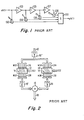
- FIGURE 1 shows a typical post-multiply or output weighted digital filter.
- the input to the digital filter consists of data samples taken once in each time period T. The samples are quantized into n-bit binary numbers.
- the input to the digital filter is x(kT) and the output is y(kT).
- the input signal x(kT) is coupled to the input of a multiplier circuit 102 which multiplies the input by a coefficient a 0 to form the product a 0 x(kT).
- the input signal is also coupled to a delay element 103 which introduces a delay of T units so that the output of delay element 103 at time kT will be x(kT-T).
- the input of multiplier 104 is coupled to the output of delay element 103.
- the output of delay element 103 is also coupled to the input of delay element 105, the output of which is coupled to the input of multiplier 106.
- the signal x(kT-2T) appears at the output of delay element 105 and the product a 2 x(kT-2T) appears at the output of multiplier 106.
- the output of delay element 105 is also coupled to the input of delay element 107, the output of which is coupled to the input of multiplier 108.
- the signal x(kT-3T) appears at the output of delay element 107 and the product a 3 x(kT-3T) appears at the output of multiplier 108.
- each of the multipliers 102, 104, 106, 108 is coupled to one input of summing circuit 109, the output of which is the output y(kT) of the digital filter.
- the filter is referred to as a "post-multiply" digital filter because multiplication is performed after the signal has been delayed.
- the speed and complexity of the digital filter will be determined primarily by the multipliers 102, 104, 106 and 108.
- the delay stages comprise a relatively small portion of the filter hardware.
- FIGURE 2 illustrates a typical shift-and-add weighting circuit.
- Parallel bit input samples are applied on bus 10. These samples are directed to bit shifting elements 12 and 14. Responsive to coefficient control signals applied to control ports CC1 and CC2, shifters 12 and 14 translate the bit positions of the samples.
- bits of the applied samples may be translated rightward or leftward, or leftward only or rightward only in accordance with the applied coefficient control signal.
- Rightward shifts effect a division by two for each bit position shifted.
- Leftward shifts effect a multiplication by two for each bit position shifted.
- Elements 12 and 14 may be barrel shifters and when used in the shift-and-add circuit permit changing of the coefficient values. Note, however, that if it is not desired to change the weighting coefficient, elements 12 and 14 may be eliminated and the bit shift performed by appropriate hardwiring.
- sample complementing circuits e.g. twos complement circuitry
- Such circuitry may be included at the input as illustrated by the box 19" drawn in dashed lines.
- complementing circuits 19 and 19' may be serially connected at the output connections of shifter elements 12 and 14.
- only one or the other of the complementing circuits 19 or 19' may be included to provide a greater variety of coefficient values. For example, if samples passed by element 12 are not bit shifted and samples passed by element 14 are shifted four bit positions and complemented, the coefficient value is 1-1/16 or 15/16.
- the samples output from shifters 12 and 14 are applied to first and second input ports of adder 16 which provides the weighted output samples at output port 18.
- the shift-and-add type of multiplier or weighting circuit produces tap weights of binary coefficients.
- the tap weights, t may be represented by the equation: where in general the A. equal zero or 1 and the number N is the maximum number of bit shifts permitted in the particular application, but where, as for the shift-and-add circuit of FIGURE 2, only two at most of the A i are permitted to equal 1. (Note, however, that if the FIGURE 2 circuit is augmented with additional shift circuits which apply additional shifted samples to adder 16, then for each additional shifter, one more of the A i coefficients may equal 1. )
- both a delayed sample and a scaled version of the delayed sample is available to the shift-and-add circuit.
- the scaled version is scaled by the factor 3/4 and that either the scaled or non-scaled sample may be applied to either or both shift circuits 12 and 14.
- the sample values available at the output ports of shift circuits 12 and 14 may therefore be weighted by the factors 0, 1, 1/2, 1/4, 1/8, 1/16, 1/32, 3/8, 3/16, 3/32, 3/64 and 3/128 (the latter 5 factors being the products of 3/4 x (1/2, 1/4, 1/8, 1/16 and 1/32).
- the number of weighting coefficients provided by this arrangement is equal to the number of unique sums of all combinations of pairs of these factors and is equal to 44.
- the resulting coefficients include 1/128 x (0, 3, 4, 6, 7, 8, 9, 10, 11, 12, 14, 15, 16, 18, 19, 20, 22, 24, 27, 28, 30, 32, 35, 36, 38, 40, 44, 48, 51, 52, 54, 56, 60, 64, 67, 68, 70, 72, 76, 80, 88, 96, 112, 128). Note that in both examples if the bit shifters may produce both positive and negative values, the number of possible positive coefficients expands slightly.
- the number of possible coefficients depends upon the scale factor chosen. For example, if a scale factor of 5/8 is used the number of coefficients increases to 50.
- the availability of large numbers of possible coefficient values realizable with simple shift-and-add weighting circuits of the type illustrated in FIGURE 2 enables the designer to synthesize relatively simple, fast FIR filters for a relatively wide range of transfer functions with good precision.
- FIGURE 3 illustrates an exemplary FIR filter having facility for applying both a scaled and an unscaled sample to the respective weighting circuits W.
- signal samples to be weighted are applied at input port 30. These samples are applied to the cascade connected delay stages 37-41 each of which has an output tap from which successively delayed signal samples are accessed.
- Input signal samples at port 30 are also applied to scaling circuit 31, which may be a shift-and-add weighting circuit, and which multiplies the samples applied thereto by a scale factor.
- Scaled signal samples from scaling circuit 31 are applied to the cascade connected delay stages 32-36.
- Delay stages 32-36 are similar to stages 37-41, and have respective output taps from which successively delayed signal samples may be accessed.
- Scaled samples from respective delay stages 32-36 and non-scaled samples from respective corresponding delay stages 37-41 are applied to respective weighting circuits 42-46.
- Weighting circuits W which may be shift-and-add circuits, responsive to selected ones of the scaled and non-scaled delayed samples, provide weighted representations of the delayed input samples.
- the weighted samples from weighting circuits 42-46 are applied to the adder circuit 47 which sums the weighted delayed samples to produce at output OUT filtered replicas of the input samples.
- FIGURE 4 illustrates an exemplary weighting circuit 45' which may be employed in the FIGURE 3 filter.
- the weighting circuit 45' is of the shift-and-add type and includes facility for programming the weighting coefficient via control signals applied to coefficient control input ports CC3 and CC4.
- the FIGURE 4 circuit is similar in form and function to that of FIGURE 2 in that it includes bit shifters 52 and 53 for performing binary weighting of the applied samples and an adder 54 to sum the binary weighted samples.
- FIGURE 4 includes first and second multiplexers 50 and 51 for applying one or the other of the scaled or non-scaled delayed input samples to either or both of the bit shifters 52 and 53 respectively.
- Weighting circuit 45' can be arranged to produce, for example, a weighting of the input samples by any of the 44 coefficients listed in the second example. Note, complementing circuits may be included in the FIGURE 4 apparatus to provide negative coefficients in an arrangement similar to that utilized in FIGURE 2.
- FIGURE 5 illustrates a hardwired version of the FIGURE 4 weighting circuit arranged to weight the input signals to be filtered by the coefficient 13/128 for the input samples scaled by the factor of 3/4.
- the multiplexers nor the programmable bit shifters are necessary.
- the illustrated circuitry is described in terms of simple shift-and-add circuitry; however, it will be appreciated that the shift-and-add circuits may be augmented with additional bit shifters and adders in an adder-tree like arrangement to further increase the number of possible weighting coefficients.
- the input scaling circuit may be designed to scale the input samples by negative factors or to selectively scale successive samples by different factors. Further, it may be necessary to include compensating delays in the non-scaled delay chain to accommodate the inherent delay of the scaling circuit.
Landscapes
- Physics & Mathematics (AREA)
- Engineering & Computer Science (AREA)
- Computer Hardware Design (AREA)
- Mathematical Physics (AREA)
- Filters That Use Time-Delay Elements (AREA)
- Cable Transmission Systems, Equalization Of Radio And Reduction Of Echo (AREA)
- Complex Calculations (AREA)
- Color Television Systems (AREA)
- Picture Signal Circuits (AREA)
- Image Processing (AREA)
- Filtering Of Dispersed Particles In Gases (AREA)
- Liquid Crystal Substances (AREA)
- Piezo-Electric Or Mechanical Vibrators, Or Delay Or Filter Circuits (AREA)
- Inks, Pencil-Leads, Or Crayons (AREA)
- Color Television Image Signal Generators (AREA)
- Developing Agents For Electrophotography (AREA)
- Investigating Or Analyzing Materials By The Use Of Electric Means (AREA)
- Electrophonic Musical Instruments (AREA)
Priority Applications (1)
| Application Number | Priority Date | Filing Date | Title |
|---|---|---|---|
| AT85300353T ATE61894T1 (de) | 1984-01-20 | 1985-01-18 | Digitaler fir-filter mit aufloesungsvermoegen bei den multiplizierkoeffizienten. |
Applications Claiming Priority (2)
| Application Number | Priority Date | Filing Date | Title |
|---|---|---|---|
| US06/572,442 US4615026A (en) | 1984-01-20 | 1984-01-20 | Digital FIR filters with enhanced tap weight resolution |
| US572442 | 1984-01-20 |
Publications (3)
| Publication Number | Publication Date |
|---|---|
| EP0150114A2 true EP0150114A2 (fr) | 1985-07-31 |
| EP0150114A3 EP0150114A3 (en) | 1987-05-20 |
| EP0150114B1 EP0150114B1 (fr) | 1991-03-20 |
Family
ID=24287821
Family Applications (1)
| Application Number | Title | Priority Date | Filing Date |
|---|---|---|---|
| EP85300353A Expired - Lifetime EP0150114B1 (fr) | 1984-01-20 | 1985-01-18 | Filtre numérique du type FIR avec des coéfficients de multiplication ayant pour effet une résolution augmentée |
Country Status (11)
| Country | Link |
|---|---|
| US (1) | US4615026A (fr) |
| EP (1) | EP0150114B1 (fr) |
| JP (1) | JP2779617B2 (fr) |
| KR (1) | KR940006211B1 (fr) |
| AT (1) | ATE61894T1 (fr) |
| AU (1) | AU572253B2 (fr) |
| CA (1) | CA1245302A (fr) |
| DE (1) | DE3582178D1 (fr) |
| ES (1) | ES539539A0 (fr) |
| FI (1) | FI83142C (fr) |
| PT (1) | PT79850B (fr) |
Cited By (2)
| Publication number | Priority date | Publication date | Assignee | Title |
|---|---|---|---|---|
| DE4022381A1 (de) * | 1989-07-14 | 1991-01-24 | Tektronix Inc | Verwendung langer digitalfilter bei vorkommnis von abrundungsfehlern |
| WO1994009564A1 (fr) * | 1992-10-13 | 1994-04-28 | Literal Corporation | Egalisation numerique dans des systemes d'enregistrement optique |
Families Citing this family (17)
| Publication number | Priority date | Publication date | Assignee | Title |
|---|---|---|---|---|
| DE3345284A1 (de) * | 1983-12-14 | 1985-06-27 | Siemens AG, 1000 Berlin und 8000 München | Verfahren und schaltungsanordnung zur digitalsignalverarbeitung nach art eines vorzugsweise adaptiven transversalfilters |
| US4615026A (en) * | 1984-01-20 | 1986-09-30 | Rca Corporation | Digital FIR filters with enhanced tap weight resolution |
| US4817025A (en) * | 1984-02-03 | 1989-03-28 | Sharp Kabushiki Kaisha | Digital filter |
| JPH0828649B2 (ja) * | 1989-02-16 | 1996-03-21 | 日本電気株式会社 | ディジタルフィルタ |
| US5018090A (en) * | 1990-03-13 | 1991-05-21 | Rca Licensing Corporation | Digital interpolation circuitry |
| SE467680B (sv) * | 1990-12-19 | 1992-08-24 | Johan Hellgren | Digital filterbank med minskad effektfoerbrukning |
| US5258939A (en) * | 1991-10-10 | 1993-11-02 | Harris Corporation | Fold and decimate filter architecture |
| US5260888A (en) * | 1992-05-28 | 1993-11-09 | Eastman Kodak Company | Shift and add digital signal processor |
| MY111506A (en) * | 1992-07-29 | 2000-07-31 | Thomson Consumer Electronics Inc | Fir filter apparatus for processing of time division multiplexed signals |
| US5592403A (en) * | 1993-03-11 | 1997-01-07 | Monolith Technologies Corporation | Digital-to-analog converter including integral digital audio filter |
| US6430287B1 (en) | 1997-03-25 | 2002-08-06 | Level One Communications, Inc. | Combined parallel adaptive equalizer/echo canceller |
| US6606641B1 (en) * | 1998-04-20 | 2003-08-12 | Koninklijke Philips Electronics N.V. | System for varying the dynamic range of coefficients in a digital filter |
| KR100400726B1 (ko) * | 1999-01-30 | 2003-10-08 | 엘지전자 주식회사 | 유한 임펄스 응답 필터 |
| US6505221B1 (en) | 1999-09-20 | 2003-01-07 | Koninklijke Philips Electronics N.V. | FIR filter utilizing programmable shifter |
| US7043513B2 (en) * | 2002-08-09 | 2006-05-09 | Terax Communication Technologies, Inc. | Clock balanced segmentation digital filter provided with optimun area of data path |
| RU2254684C1 (ru) * | 2004-01-08 | 2005-06-20 | Общество с ограниченной ответственностью "Информационный Вычислительный Центр" | Цифровое устройство символьной синхронизации |
| US10277202B2 (en) * | 2016-07-14 | 2019-04-30 | Texas Instruments Incorporated | Methods and apparatus for efficient linear combiner |
Family Cites Families (15)
| Publication number | Priority date | Publication date | Assignee | Title |
|---|---|---|---|---|
| US3521042A (en) * | 1967-07-19 | 1970-07-21 | Ibm | Simplified digital filter |
| US3696235A (en) * | 1970-06-22 | 1972-10-03 | Sanders Associates Inc | Digital filter using weighting |
| FR2250239B1 (fr) * | 1973-10-23 | 1976-07-02 | Ibm France | |
| US3979701A (en) * | 1975-06-17 | 1976-09-07 | Communications Satellite Corporation (Comsat) | Non-recursive digital filter employing simple coefficients |
| FR2331213A1 (fr) * | 1975-11-10 | 1977-06-03 | Ibm France | Filtre numerique |
| FR2379946A1 (fr) * | 1977-02-04 | 1978-09-01 | Labo Cent Telecommunicat | Filtre numerique |
| JPS53137652A (en) * | 1977-05-07 | 1978-12-01 | Fujitsu Ltd | Ccd transversal of digital coefficient type |
| US4191853A (en) * | 1978-10-10 | 1980-03-04 | Motorola Inc. | Sampled data filter with time shared weighters for use as an LPC and synthesizer |
| JPS55117322A (en) * | 1979-03-02 | 1980-09-09 | Fujitsu Ltd | Binary transversal filter |
| NL7905332A (nl) * | 1979-07-09 | 1981-01-13 | Philips Nv | Decimerend, lineair phase, digital fir filter. |
| JPS5698022A (en) * | 1980-01-07 | 1981-08-07 | Nec Corp | Difference coefficient digital filter |
| GB2095067B (en) * | 1981-03-12 | 1984-10-03 | Standard Telephones Cables Ltd | Digital filter arrangement |
| US4524423A (en) * | 1981-11-06 | 1985-06-18 | Rca Corporation | Digital signal separation filters |
| NL8203520A (nl) * | 1982-09-10 | 1984-04-02 | Philips Nv | Digitale filterinrichting. |
| US4615026A (en) * | 1984-01-20 | 1986-09-30 | Rca Corporation | Digital FIR filters with enhanced tap weight resolution |
-
1984
- 1984-01-20 US US06/572,442 patent/US4615026A/en not_active Expired - Fee Related
-
1985
- 1985-01-11 AU AU37613/85A patent/AU572253B2/en not_active Ceased
- 1985-01-11 CA CA000471969A patent/CA1245302A/fr not_active Expired
- 1985-01-14 ES ES539539A patent/ES539539A0/es active Granted
- 1985-01-14 FI FI850152A patent/FI83142C/fi not_active IP Right Cessation
- 1985-01-18 EP EP85300353A patent/EP0150114B1/fr not_active Expired - Lifetime
- 1985-01-18 DE DE8585300353T patent/DE3582178D1/de not_active Expired - Fee Related
- 1985-01-18 AT AT85300353T patent/ATE61894T1/de not_active IP Right Cessation
- 1985-01-18 KR KR1019850000287A patent/KR940006211B1/ko not_active Expired - Fee Related
- 1985-01-18 JP JP60006021A patent/JP2779617B2/ja not_active Expired - Lifetime
- 1985-01-18 PT PT79850A patent/PT79850B/pt not_active IP Right Cessation
Cited By (3)
| Publication number | Priority date | Publication date | Assignee | Title |
|---|---|---|---|---|
| DE4022381A1 (de) * | 1989-07-14 | 1991-01-24 | Tektronix Inc | Verwendung langer digitalfilter bei vorkommnis von abrundungsfehlern |
| WO1994009564A1 (fr) * | 1992-10-13 | 1994-04-28 | Literal Corporation | Egalisation numerique dans des systemes d'enregistrement optique |
| US5586100A (en) * | 1992-10-13 | 1996-12-17 | Literal Corporation | Transversal filter and method for cancelling intersymbol interference |
Also Published As
| Publication number | Publication date |
|---|---|
| FI83142B (fi) | 1991-02-15 |
| ES8602319A1 (es) | 1985-11-16 |
| JP2779617B2 (ja) | 1998-07-23 |
| PT79850A (en) | 1985-02-01 |
| ATE61894T1 (de) | 1991-04-15 |
| JPS60229419A (ja) | 1985-11-14 |
| FI850152L (fi) | 1985-07-21 |
| EP0150114B1 (fr) | 1991-03-20 |
| AU572253B2 (en) | 1988-05-05 |
| PT79850B (en) | 1986-09-11 |
| ES539539A0 (es) | 1985-11-16 |
| CA1245302A (fr) | 1988-11-22 |
| FI83142C (fi) | 1991-05-27 |
| KR940006211B1 (ko) | 1994-07-11 |
| US4615026A (en) | 1986-09-30 |
| KR850005748A (ko) | 1985-08-28 |
| AU3761385A (en) | 1985-07-25 |
| FI850152A0 (fi) | 1985-01-14 |
| DE3582178D1 (de) | 1991-04-25 |
| EP0150114A3 (en) | 1987-05-20 |
Similar Documents
| Publication | Publication Date | Title |
|---|---|---|
| EP0150114B1 (fr) | Filtre numérique du type FIR avec des coéfficients de multiplication ayant pour effet une résolution augmentée | |
| US5262974A (en) | Programmable canonic signed digit filter chip | |
| US3665171A (en) | Nonrecursive digital filter apparatus employing delayedadd configuration | |
| US3521041A (en) | Digital filters | |
| US5511015A (en) | Double-accumulator implementation of the convolution function | |
| US6009448A (en) | Pipelined parallel-serial architecture for a modified least mean square adaptive filter | |
| EP0583927A1 (fr) | Système d'equilibreur dynamiquement adaptable et méthode | |
| EP0372350B1 (fr) | Filtre numérique programmable | |
| GB2137839A (en) | Digital signal processors | |
| JPH0661792A (ja) | デジタル・フィルタ | |
| US4791597A (en) | Multiplierless FIR digital filter with two to the Nth power coefficients | |
| EP0182602B1 (fr) | Filtre numérique | |
| EP0693236B1 (fr) | Procede et structure de filtre fir numerique transpose destine a multiplier un signal d'entree binaire par des coefficents et procede de conception d'un filtre numerique transpose | |
| EP0373468A2 (fr) | Processeur pipeline pour mettre en oeuvre l'algorithme de LMS | |
| US5805479A (en) | Apparatus and method for filtering digital signals | |
| US4893264A (en) | Digital decimation filter | |
| US4012628A (en) | Filter with a reduced number of shift register taps | |
| EP0791242B1 (fr) | Filtre numerique ameliore | |
| US3725686A (en) | Polyphasor generation by vector addition and scalar multiplication | |
| US6938063B2 (en) | Programmable filter architecture | |
| Eskritt et al. | A 2-digit DBNS filter architecture | |
| Rader | On digital filtering | |
| US5148384A (en) | Signal processing integrated circuit | |
| US5912827A (en) | Digital filter with low rolloff factor | |
| EP0266004A2 (fr) | Filtre numérique non récursif avec des coefficients de multiplication du type puissance-deux |
Legal Events
| Date | Code | Title | Description |
|---|---|---|---|
| PUAI | Public reference made under article 153(3) epc to a published international application that has entered the european phase |
Free format text: ORIGINAL CODE: 0009012 |
|
| AK | Designated contracting states |
Designated state(s): AT DE FR GB IT |
|
| PUAL | Search report despatched |
Free format text: ORIGINAL CODE: 0009013 |
|
| AK | Designated contracting states |
Kind code of ref document: A3 Designated state(s): AT DE FR GB IT |
|
| 17P | Request for examination filed |
Effective date: 19871021 |
|
| RAP1 | Party data changed (applicant data changed or rights of an application transferred) |
Owner name: RCA LICENSING CORPORATION |
|
| 17Q | First examination report despatched |
Effective date: 19900418 |
|
| GRAA | (expected) grant |
Free format text: ORIGINAL CODE: 0009210 |
|
| AK | Designated contracting states |
Kind code of ref document: B1 Designated state(s): AT DE FR GB IT |
|
| REF | Corresponds to: |
Ref document number: 61894 Country of ref document: AT Date of ref document: 19910415 Kind code of ref document: T |
|
| ITF | It: translation for a ep patent filed | ||
| REF | Corresponds to: |
Ref document number: 3582178 Country of ref document: DE Date of ref document: 19910425 |
|
| ET | Fr: translation filed | ||
| PLBE | No opposition filed within time limit |
Free format text: ORIGINAL CODE: 0009261 |
|
| STAA | Information on the status of an ep patent application or granted ep patent |
Free format text: STATUS: NO OPPOSITION FILED WITHIN TIME LIMIT |
|
| 26N | No opposition filed | ||
| PGFP | Annual fee paid to national office [announced via postgrant information from national office to epo] |
Ref country code: AT Payment date: 19951211 Year of fee payment: 12 |
|
| PG25 | Lapsed in a contracting state [announced via postgrant information from national office to epo] |
Ref country code: AT Effective date: 19970118 |
|
| PGFP | Annual fee paid to national office [announced via postgrant information from national office to epo] |
Ref country code: DE Payment date: 19981202 Year of fee payment: 15 |
|
| PGFP | Annual fee paid to national office [announced via postgrant information from national office to epo] |
Ref country code: GB Payment date: 19981204 Year of fee payment: 15 |
|
| PGFP | Annual fee paid to national office [announced via postgrant information from national office to epo] |
Ref country code: FR Payment date: 19981207 Year of fee payment: 15 |
|
| PG25 | Lapsed in a contracting state [announced via postgrant information from national office to epo] |
Ref country code: GB Free format text: LAPSE BECAUSE OF NON-PAYMENT OF DUE FEES Effective date: 20000118 |
|
| GBPC | Gb: european patent ceased through non-payment of renewal fee |
Effective date: 20000118 |
|
| PG25 | Lapsed in a contracting state [announced via postgrant information from national office to epo] |
Ref country code: FR Free format text: LAPSE BECAUSE OF NON-PAYMENT OF DUE FEES Effective date: 20000929 |
|
| PG25 | Lapsed in a contracting state [announced via postgrant information from national office to epo] |
Ref country code: DE Free format text: LAPSE BECAUSE OF NON-PAYMENT OF DUE FEES Effective date: 20001101 |
|
| REG | Reference to a national code |
Ref country code: FR Ref legal event code: ST |