EP0150564A2 - Elektronische Vorrichtung mit einem Heteroübergang - Google Patents
Elektronische Vorrichtung mit einem Heteroübergang Download PDFInfo
- Publication number
- EP0150564A2 EP0150564A2 EP84307100A EP84307100A EP0150564A2 EP 0150564 A2 EP0150564 A2 EP 0150564A2 EP 84307100 A EP84307100 A EP 84307100A EP 84307100 A EP84307100 A EP 84307100A EP 0150564 A2 EP0150564 A2 EP 0150564A2
- Authority
- EP
- European Patent Office
- Prior art keywords
- region
- bandgap
- electric field
- avalanche
- regions
- Prior art date
- Legal status (The legal status is an assumption and is not a legal conclusion. Google has not performed a legal analysis and makes no representation as to the accuracy of the status listed.)
- Withdrawn
Links
- 230000005684 electric field Effects 0.000 claims description 45
- 239000004065 semiconductor Substances 0.000 claims description 13
- 150000001875 compounds Chemical class 0.000 claims description 9
- 239000000463 material Substances 0.000 claims description 8
- 230000015556 catabolic process Effects 0.000 claims description 7
- 230000007704 transition Effects 0.000 claims description 7
- 229910052732 germanium Inorganic materials 0.000 claims description 4
- 229910052710 silicon Inorganic materials 0.000 claims description 4
- 238000010521 absorption reaction Methods 0.000 abstract description 8
- 230000035945 sensitivity Effects 0.000 abstract 1
- 239000010410 layer Substances 0.000 description 17
- 230000005641 tunneling Effects 0.000 description 11
- 239000013545 self-assembled monolayer Substances 0.000 description 8
- 239000002184 metal Substances 0.000 description 5
- 229910052751 metal Inorganic materials 0.000 description 5
- 230000003287 optical effect Effects 0.000 description 5
- XUIMIQQOPSSXEZ-UHFFFAOYSA-N Silicon Chemical group [Si] XUIMIQQOPSSXEZ-UHFFFAOYSA-N 0.000 description 4
- 238000001465 metallisation Methods 0.000 description 4
- 238000000034 method Methods 0.000 description 4
- 239000000203 mixture Substances 0.000 description 4
- 230000005855 radiation Effects 0.000 description 4
- 230000008569 process Effects 0.000 description 3
- 239000000758 substrate Substances 0.000 description 3
- 239000011358 absorbing material Substances 0.000 description 2
- 238000000098 azimuthal photoelectron diffraction Methods 0.000 description 2
- 230000007423 decrease Effects 0.000 description 2
- 238000013461 design Methods 0.000 description 2
- 239000002019 doping agent Substances 0.000 description 2
- GNPVGFCGXDBREM-UHFFFAOYSA-N germanium atom Chemical compound [Ge] GNPVGFCGXDBREM-UHFFFAOYSA-N 0.000 description 2
- 239000012212 insulator Substances 0.000 description 2
- 239000010703 silicon Substances 0.000 description 2
- 229910000530 Gallium indium arsenide Inorganic materials 0.000 description 1
- 229910052581 Si3N4 Inorganic materials 0.000 description 1
- 238000004458 analytical method Methods 0.000 description 1
- 238000013459 approach Methods 0.000 description 1
- 229910052785 arsenic Inorganic materials 0.000 description 1
- 230000004888 barrier function Effects 0.000 description 1
- 230000005540 biological transmission Effects 0.000 description 1
- 239000000969 carrier Substances 0.000 description 1
- 230000008859 change Effects 0.000 description 1
- 238000005229 chemical vapour deposition Methods 0.000 description 1
- 238000007796 conventional method Methods 0.000 description 1
- 230000003247 decreasing effect Effects 0.000 description 1
- 238000009792 diffusion process Methods 0.000 description 1
- 239000011521 glass Substances 0.000 description 1
- 238000004519 manufacturing process Methods 0.000 description 1
- 238000012986 modification Methods 0.000 description 1
- 230000004048 modification Effects 0.000 description 1
- 238000001451 molecular beam epitaxy Methods 0.000 description 1
- 239000013307 optical fiber Substances 0.000 description 1
- 230000004044 response Effects 0.000 description 1
- 238000000682 scanning probe acoustic microscopy Methods 0.000 description 1
- 238000000927 vapour-phase epitaxy Methods 0.000 description 1
Images

Classifications
-
- H—ELECTRICITY
- H10—SEMICONDUCTOR DEVICES; ELECTRIC SOLID-STATE DEVICES NOT OTHERWISE PROVIDED FOR
- H10F—INORGANIC SEMICONDUCTOR DEVICES SENSITIVE TO INFRARED RADIATION, LIGHT, ELECTROMAGNETIC RADIATION OF SHORTER WAVELENGTH OR CORPUSCULAR RADIATION
- H10F30/00—Individual radiation-sensitive semiconductor devices in which radiation controls the flow of current through the devices, e.g. photodetectors
- H10F30/20—Individual radiation-sensitive semiconductor devices in which radiation controls the flow of current through the devices, e.g. photodetectors the devices having potential barriers, e.g. phototransistors
- H10F30/21—Individual radiation-sensitive semiconductor devices in which radiation controls the flow of current through the devices, e.g. photodetectors the devices having potential barriers, e.g. phototransistors the devices being sensitive to infrared, visible or ultraviolet radiation
- H10F30/22—Individual radiation-sensitive semiconductor devices in which radiation controls the flow of current through the devices, e.g. photodetectors the devices having potential barriers, e.g. phototransistors the devices being sensitive to infrared, visible or ultraviolet radiation the devices having only one potential barrier, e.g. photodiodes
- H10F30/222—Individual radiation-sensitive semiconductor devices in which radiation controls the flow of current through the devices, e.g. photodetectors the devices having potential barriers, e.g. phototransistors the devices being sensitive to infrared, visible or ultraviolet radiation the devices having only one potential barrier, e.g. photodiodes the potential barrier being a PN heterojunction
-
- H—ELECTRICITY
- H10—SEMICONDUCTOR DEVICES; ELECTRIC SOLID-STATE DEVICES NOT OTHERWISE PROVIDED FOR
- H10F—INORGANIC SEMICONDUCTOR DEVICES SENSITIVE TO INFRARED RADIATION, LIGHT, ELECTROMAGNETIC RADIATION OF SHORTER WAVELENGTH OR CORPUSCULAR RADIATION
- H10F30/00—Individual radiation-sensitive semiconductor devices in which radiation controls the flow of current through the devices, e.g. photodetectors
- H10F30/20—Individual radiation-sensitive semiconductor devices in which radiation controls the flow of current through the devices, e.g. photodetectors the devices having potential barriers, e.g. phototransistors
- H10F30/21—Individual radiation-sensitive semiconductor devices in which radiation controls the flow of current through the devices, e.g. photodetectors the devices having potential barriers, e.g. phototransistors the devices being sensitive to infrared, visible or ultraviolet radiation
- H10F30/22—Individual radiation-sensitive semiconductor devices in which radiation controls the flow of current through the devices, e.g. photodetectors the devices having potential barriers, e.g. phototransistors the devices being sensitive to infrared, visible or ultraviolet radiation the devices having only one potential barrier, e.g. photodiodes
- H10F30/225—Individual radiation-sensitive semiconductor devices in which radiation controls the flow of current through the devices, e.g. photodetectors the devices having potential barriers, e.g. phototransistors the devices being sensitive to infrared, visible or ultraviolet radiation the devices having only one potential barrier, e.g. photodiodes the potential barrier working in avalanche mode, e.g. avalanche photodiodes
- H10F30/2255—Individual radiation-sensitive semiconductor devices in which radiation controls the flow of current through the devices, e.g. photodetectors the devices having potential barriers, e.g. phototransistors the devices being sensitive to infrared, visible or ultraviolet radiation the devices having only one potential barrier, e.g. photodiodes the potential barrier working in avalanche mode, e.g. avalanche photodiodes in which the active layers form heterostructures, e.g. SAM structures
Definitions
- This invention relates to electronic devices and finds application, for example, in heterojunction photodetectors.
- photodetectors that have characteristics such as rapid response times and low noise. While such photodetectors have many possible applications, one application of special interest today is in optical communications systems. Such systems, as presently contemplated, have a light source and a photodetector optically coupled to each other by a glass transmission line which is commonly called an optical fiber.
- Avalanche photodetectors exhibit current gain because of avalanche multiplication initiated by at least one type of carrier.
- An early example of such a photodetector is described in IEEE Transactions on Electron Devices, ED-14, pp.239-251, May 1967.
- the silicon structure described has a p+-i-p-n+ doping profile and was termed a reach-through avalanche photodetector (RAPD) because the electric field extended from the n+-p avalanche region on one side of the device through an intrinsic region to the p+ layer which functioned as an ohmic contact on the other side of the device.
- RAPD avalanche photodetector
- the doping profile was similar to that of a Read diode or that of an IMPATT diode.
- avalanche photodetectors While the first avalanche photodetectors brought to a high degree of perfection used elemental semiconductors such as silicon or germanium, avalanche photodetectors have also been proposed using numerous other semiconductors including various Group III-V compound semiconductors. Interest in APDs using such semiconductors has increased as interest in optical communications systems has shifted from those using wavelengths near 0.8 um to those using longer wavelengths, particularly wavelengths in the region between 1.0 ⁇ m and 1.6 um, because silicon photodetectors are not sensitive to radiation within this wavelength region and germanium AP D s are noisy.
- Ga 0.47 In 0.53 As As the light absorbing material which is grown lattice matched to a substrate comprising a Group III-V semiconductor such as InP.
- Ga 0.47 In 0.53 As is a desirable material for optical communications systems because it is sensitive to, i.e., absorbs, radiation having wavelengths less than 1.7 um, i.e., wavelengths within the region between 1.0 um and 1.6 um.
- the dark current at a high electric field i.e., 10 5 V/ cm or greater
- a tunneling current which increases as the energy bandgap decreases. That is, the small bandgap which is advantageous as it enables the Ga 0.47 In 0.53 As to absorb long wavelength radiation is also disadvantageous as it leads to an increased dark current in avalanche photodetectors.
- the dark current is also large in Ga 0.4 7In 0.53 As because of the small electron effective mass.
- the tunneling current was reduced, with respect to an all Ga 0.47 In 0.53 As device, because the avalanche process took place in a portion of the high bandgap region spaced from the heterointerface, and the electric field at the heterojunction was thus less than the field in the avalanche region and lower than the typical field required for tunneling in Ga 0.47 In 0.53 As.
- the device thus has separate absorption and multiplication regions and is commonly referred to as a SAM, which is an acronym for Separate Absorption and Multiplication regions.
- SAM Separate Absorption and Multiplication regions
- the maximum electric field, E m in the n-type InP region must be large enough, at least 4.5 x 10 5 V/cm, for the desired avalanche gain to occur.
- Reference to their FIG. 2 also shows that ⁇ B, the charge density per unit area depleted in the n-type InP region, must be at least 2 x 10 12 cm-2.
- ⁇ B is too large, i.e. greater than 3 x 101 2 cm-2, the InP is not completely depleted at breakdown and the photodetector has low quantum efficiency.
- an electronic device includes a low bandgap region, a high bandgap region, the low bandgap region and the high bandgap region having a common interface, and first and second electrical contacts to the high bandgap region and to the low bandgap region, respectively, the high bandgap region including a first region having an electric field such that the avalanche gain is greater than 1.0 under appropriate bias conditions and a first electric field gradient, and a second region having an electric field less than the breakdown field under appropriate bias conditions and a second electric field gradient, the first region being spaced from the interface of the high bandgap region and the low bandgap region by the second region.
- the second region's electric field is such that the avalanche gain is greater than 1.0 and greater than the first region's electric field.
- the second region is more heavily doped than the first region.
- the first region is more heavily doped than the second region.
- the second region comprises a very lightly doped, either u or n conductivity, region and there is a transition region which comprises a thin heavily doped region between the first and second regions.
- the heavily doped transition region is spaced from the interface between the high bandgap and the low bandgap regions by a lightly doped, either conductivity type, region which forms the first region.
- the high bandgap region comprises Al 0.48 In 0.52 As or InP and the low bandgap region comprises Ga 0.47 In 0.53 As.
- the incident radiation is absorbed in the low bandgaop region and avalanche multiplication occurs in that portion of the high bandgap region where the field is of the order of the breakdown field.
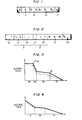
- An exemplary device schematically depicted in section in FIG. 1 comprises a first high bandgap region 11 which has, under appropriate bias conditions, a first electric field such that the avalanche gain is greater than 1.0, a second high bandgap region 21 which has a second electric field which is less than the breakdown field and the first electric field, and a low bandgap region 31.
- the first and second high bandgap regions have first and second electric field gradients, respectively.
- region 11 is more heavily doped than is region 21.
- region 21 is more heavily doped than is region 11.
- the first region 11, which has the higher electric field, is spaced from the interface of regions 21 and 31.
- the device further comprises regions 1 and 3 which form electrical contacts to regions 11 and 31, respectively.
- Region 1 may comprise a metal or a metal and a heavily doped region.
- Region 3 comprises a metal and a heavily doped region.
- the low bandgap region 31 is an absorption region and the high bandgap regions 11 and 21 form the multiplication region, although, as will be readily appreciated by those skilled in the art, avalanche gain occurs in only a portion of these regions.
- the terms "electric field”, “electric field gradient”, and “bandgap” refer to average values within each region as the regions may have, for example, compositional or doping nonuniformities, which result in nonuniform bandgaps or electric fields within the regions.
- the avalanche region i.e., the region in which avalanche gain occurs, may be relatively thick as the electric field in the high field may be nearly constant, i.e., it has a small gradient, and is certainly significantly smaller than in the avalanche region of a conventional SAM APD.
- the total gain is relatively large, but it is not obtained at the expense of a large interface field; thus, the dark current may be minimized.
- the lower electric field in the avalanche region reduces the excess noise factor.
- the device depicted comprises regions 101, which is a metal. and 103, which has a highly doped region and a metal.
- Region 111 is highly doped and has a conductivity type opposite that of region 103. Region 111 may be omitted for a Schottky barrier device.
- Regions 101 and 111 form a first electrical contact region and region 103 forms a second electrical contact region.
- regions 11, 21, and 31 there are regions 11, 21, and 31. Regions 21 and 31 contact each other, i.e., they have an interface.
- the high bandgap region comprises region 111 which is highly doped and has a first conductivity type, region 113 which is of intrinsic, v or n, conductivity, region 211 which is heavily doped and of a second conductivity type, and region 213 which has intrinsic conductivity. Region 213 is desirable to avoid having a heavily doped region at the interface. Regions 113, 211, and 213 are the first , transition, and secondregions, respectively. Region 211 has a thickness Ax and is spaced from the interface of regions 21 and 31. Region 31 has a low bandgap and a second conductivity type and is preferably intrinsic.
- intrinsic conductivity means that the regions are not intentionally, or are very lightly, doped and typically have a dopant concentration less than 10 15 cm -3 , i.e., they are either v or x.
- Region 111 typically has a doping concentration typically between 10 18 and 10 19 cm -3 and a thickness between 1 and 2 um.
- Region 113 has intrinsic conductivity, that is, the doping concentration should be less than 10 15 cm -3 and has a thickness between 100 nm and several um.
- Region 211 has a doping concentration typically between 10 16 cm -3 and 5 x 10 18 cm -3 and a thickness that is typically between 5 and 500 nm.
- Region 213 has values for the doping that are generally the same as region 113, although it is in general much thinner, for example, as thin as 10 nm, and this region should also preferably be punched through under avalanche conditions.
- Region 31 has a doping concentration between 5 x 10 14 and 5 x 10 16 cm -3 . Region 31 may be punched through. However, punchthrough should occur before the onset of sizable gain. Regions 113, 213, and 31 need not have intrinsic conductivity. However, if they are doped, the doping concentration should preferably be less than that of region 211, and these regions should also be preferably punched through under avalanche conditions.
- the conductivity types of the regions depend upon the relative values of a and B, i.e., the ionization coefficients for electrons and holes, respectively. That is, the conductivity types should be selected so that the carrier having the higher ionization coefficient initiates the avalanche process.
- appropriate conductivity types are: 111-p + ; 113-v or n - ; 211-n + ; 213-v or n - ; 31-v or n - : and 103-n + .
- Si/Ge all of these conductivity types should be reversed.
- Devices embodying the invention may be grown with conventional and well-known growth techniques, such as vapor phase epitaxy, molecular beam epitaxy, or a metallo-organic chemical vapor deposition.
- Regions 111, 113, 211, and 213 may comprise, for example, Al 0.48 In 0.52 As, and region 31 may comprise, for example, Ga 0.47 In 0.53 As.
- Other Group III-V or Group II-VI compound semiconductors, as well as Si and Ge may be used.
- the electrical contacts are formed by using conventional techniques that are well known to those skilled in the art.
- FIG. 3 shows the electric field in the several regions of the device depicted in FIG. 2 vertically in arbitrary units versus the distance along the axis of the device horizontally.
- the electric field indicated by the solid line is the idealized electric field and the dashed line indicates the electric field that is more likely to be realized.
- the electric field decreases rapidly in transition region 211 from its maximum value, E max to a value close to the value of the interface field value, E i . It can also be that the maximum electric field region can be maintained over a wide region.
- the structure described may be termed a "high-low SAM,” and it has several desirable attributes. For example, a significantly lower electric field, E al is required in the avalanche region than in a conventional SAM because the avalanche process can occur over a wider region. In an InP avalanche region, the field can be reduced by a factor of 2 with respect to the peak electric field of a conventional SAM APD, and the desired high gain is obtained by using a relatively thick avalanche region.
- the selection of a low E a enables the value of the interface field, E i' to be significantly lower than the tunneling field, E it and less to a lower excess avalanche noise factor than is present in a conventional SAM APD.
- the device comprises InP/Ga 0.47 In 0.53 As regions.
- E 2 is 1 x 10 5 V/cm
- E 1 is 4 x 10 5 V/cm.
- the width of the avalanche region is 1.7 um and its doping is preferably lower than 10 15 cm -3 .
- the charge density is 2 . 2 x 10 12 cm -2 . This density may be obtained with a doping concentration of approximately 5 x 10 17 cm -3 , within region 211, and a width of approximately 44 nm.
- the thickness of the absorption region i.e., region 31, is 2 um and the doping is typically between 5 x 10 14 cm -3 and 2 x 10 15 .
- the thickness is determined by the absorption coefficient and the doping should be low to allow punchthrough of the region before the onset of gain and to permit an interface field less than the tunneling field before punchthrough.
- the thickness of region 213 is not generally critical and is typically between 20 and 300 nm.
- a portion of region 31 adjacent to the interface with region 213 may have a graded bandgap or a bandgap between that of region 213 and the remainder of region 31 to reduce carrier trapping at the interface.
- a typical material for this portion is InGaAsP of varying composition over a distance of 50 to 200 nm.
- a wide range of electric fields in region 113 may be obtained by simply changing the position and doping concentration of region 211.
- the ability to use a relatively low electric field in the avalanche gain region arises from the fact that the electric field is constant, rather than linearly decreasing as in prior art SAMs. Gain stability against voltage fluctuations is also increased when the low gap layer is punched through before the onset of gain.
- regions 11, 21, and 31 are depicted in FIG. 4 of yet another embodiment with the electric field plotted vertically in arbitrary units.
- the gradients depicted are exemplary and may be modified by those skilled in the art.
- region 11 is depicted as having a larger gradient than region 21, devices embodying the invention may be fabricated with region 21 having the larger gradient.
- Gains greater than 60 were obtained with a voltage of 25 volts and a dark current less than 10 Amp at unity gain before the onset of multiplication in an Al 0.48 In 0.52 As/Ga 0.53 In 0.47 As device depicted in a sectional view in FIG. 5.
- the device comprises a p + -Al 0.48 In 0.52 As layer 111 which is 1 to 2 um thick and a doping concentration between 10 18 and 10 19 cm -3 ; a ⁇ -Al 0.48 In 0.52 As layer 113 which is 500 nm thick; a n + -Al 0.48 In 0.52 As layer 211 which has a 5 x 10 17 cm 3 doping concentration and is 50 nm thick; a ⁇ -Al 0.48 In 0.52 As layer 213 which is 300 nm thick: a Ga 0.47 In 0.53 As layer 31 which has a 5 x 10 15 doping concentration and has a 1-2 um thickness; and an n + layer or substrate 103 which has a 5 x 10 18 cm -3 doping concentration.
- the preferred dopant for layer 211 is Si.
- the device also comprises layer 91 which is highly doped In 0.53 Ga 0.47 As and is contacted by metallization 93, such as alloyed Au/Be and evaporated Ti.
- the device comprises region 111 which is p + Cd-doped by diffusion, 10 18 -10 19 cm -3 , I nP; region 113 which is v-InP; region 211 which is n + S i-doped, 10 17 -10 19 cm -3 and, typically, 5 to 500 nm thick, InP; region 213 which is v-type InP and is between 10 and 100 nm thick and region 31 which is n + or v InGaAs and approximately 2 ⁇ m thick.
- the regions are disposed over n + buffer layer and substrate 81 which is contacted by metallization 83.
- Guard ring 121 has a conductivity type opposite to that of region 111.
- Region 111 is contacted by metallization 73 which is separated from region 113 by insulator 71.
- Metallization 73 is conventional, e.g., Au/Be and Ti, and insulator 73 is conventional, such as Si 3 N 4 .
- region 213 may be omitted.
- the avalanche region 11 as well as region 31 may have one or more graded bandgap layers, a quantum well structure, or superlattice structure, etc.
- the superlattice structure may have a constant or varying period. It will be readily appreciated that if graded bandgap layers are present in the absorption region, they are compositionally graded so that the high bandgap portion of region 31 is adjacent region 21.
- the graded region comprises, in one embodiment, a first plurality of layers of a first compound semiconductor interleaved with a second plurality of a second compound semiconductor.
- the average composition of a series of epitaxial layers is equal to the desired graded composition. It will be readily appreciated that the compositions of the first and second pluralities change to accomplish the grading. Continuous grading may also be used. These embodiments are useful when charge trapping at the interface of regions 21 and 31 limits device speed.
- devices embodying the invention may be used as IMPATT diodes with the low bandgap region being the drift region and the high bandgap region being the avalanche region.
Landscapes
- Light Receiving Elements (AREA)
Applications Claiming Priority (2)
| Application Number | Priority Date | Filing Date | Title |
|---|---|---|---|
| US54594583A | 1983-10-26 | 1983-10-26 | |
| US545945 | 1983-10-26 |
Publications (2)
| Publication Number | Publication Date |
|---|---|
| EP0150564A2 true EP0150564A2 (de) | 1985-08-07 |
| EP0150564A3 EP0150564A3 (de) | 1986-05-14 |
Family
ID=24178181
Family Applications (1)
| Application Number | Title | Priority Date | Filing Date |
|---|---|---|---|
| EP84307100A Withdrawn EP0150564A3 (de) | 1983-10-26 | 1984-10-17 | Elektronische Vorrichtung mit einem Heteroübergang |
Country Status (2)
| Country | Link |
|---|---|
| EP (1) | EP0150564A3 (de) |
| JP (1) | JPS60110179A (de) |
Cited By (5)
| Publication number | Priority date | Publication date | Assignee | Title |
|---|---|---|---|---|
| US8269222B2 (en) | 2010-05-25 | 2012-09-18 | The United States Of America As Represented By The Secretary Of The Army | Semiconductor photodetector with transparent interface charge control layer and method thereof |
| US8269223B2 (en) | 2010-05-27 | 2012-09-18 | The United States Of America As Represented By The Secretary Of The Army | Polarization enhanced avalanche photodetector and method thereof |
| US9379271B2 (en) | 2013-05-24 | 2016-06-28 | The United States Of America As Represented By The Secretary Of The Army | Variable range photodetector and method thereof |
| US9893227B2 (en) | 2013-05-24 | 2018-02-13 | The United States Of America As Represented By The Secretary Of The Army | Enhanced deep ultraviolet photodetector and method thereof |
| US11450782B2 (en) * | 2020-09-03 | 2022-09-20 | Marvell Asia Pte Ltd. | Germanium-on-silicon avalanche photodetector in silicon photonics platform, method of making the same |
Family Cites Families (4)
| Publication number | Priority date | Publication date | Assignee | Title |
|---|---|---|---|---|
| JPS52101990A (en) * | 1976-02-21 | 1977-08-26 | Hitachi Ltd | Semiconductor device for photoelectric transducer and its manufacture |
| US4383269A (en) * | 1980-09-19 | 1983-05-10 | Bell Telephone Laboratories, Incorporated | Graded bandgap photodetector |
| JPS5793585A (en) * | 1980-12-02 | 1982-06-10 | Fujitsu Ltd | Semiconductor photoreceiving element |
| FR2518817A1 (fr) * | 1981-12-23 | 1983-06-24 | Thomson Csf | Photodiode a zones d'absorption et d'avalanche separees |
-
1984
- 1984-10-17 EP EP84307100A patent/EP0150564A3/de not_active Withdrawn
- 1984-10-26 JP JP59224261A patent/JPS60110179A/ja active Pending
Cited By (6)
| Publication number | Priority date | Publication date | Assignee | Title |
|---|---|---|---|---|
| US8269222B2 (en) | 2010-05-25 | 2012-09-18 | The United States Of America As Represented By The Secretary Of The Army | Semiconductor photodetector with transparent interface charge control layer and method thereof |
| US8269223B2 (en) | 2010-05-27 | 2012-09-18 | The United States Of America As Represented By The Secretary Of The Army | Polarization enhanced avalanche photodetector and method thereof |
| US9379271B2 (en) | 2013-05-24 | 2016-06-28 | The United States Of America As Represented By The Secretary Of The Army | Variable range photodetector and method thereof |
| US9893227B2 (en) | 2013-05-24 | 2018-02-13 | The United States Of America As Represented By The Secretary Of The Army | Enhanced deep ultraviolet photodetector and method thereof |
| US11450782B2 (en) * | 2020-09-03 | 2022-09-20 | Marvell Asia Pte Ltd. | Germanium-on-silicon avalanche photodetector in silicon photonics platform, method of making the same |
| US12336308B2 (en) | 2020-09-03 | 2025-06-17 | Marvell Asia Pte Ltd | Germanium-on-silicon avalanche photodetector in silicon photonics platform, method of making the same |
Also Published As
| Publication number | Publication date |
|---|---|
| JPS60110179A (ja) | 1985-06-15 |
| EP0150564A3 (de) | 1986-05-14 |
Similar Documents
| Publication | Publication Date | Title |
|---|---|---|
| US4476477A (en) | Graded bandgap multilayer avalanche photodetector with energy step backs | |
| US5576559A (en) | Heterojunction electron transfer device | |
| US4383269A (en) | Graded bandgap photodetector | |
| US4665277A (en) | Floating emitter solar cell | |
| US4353081A (en) | Graded bandgap rectifying semiconductor devices | |
| US5679963A (en) | Semiconductor tunnel junction with enhancement layer | |
| US4794440A (en) | Heterojunction bipolar transistor | |
| US6831309B2 (en) | Unipolar photodiode having a schottky junction contact | |
| JP2845081B2 (ja) | 半導体受光素子 | |
| JPH06105789B2 (ja) | 光検出器 | |
| US4390889A (en) | Photodiode having an InGaAs layer with an adjacent InGaAsP p-n junction | |
| EP0171531A1 (de) | Halbleiteranordnung mit hoher Elektronenmobilität | |
| US4694318A (en) | Sawtooth photodetector | |
| US4825264A (en) | Resonant tunneling semiconductor device | |
| US4974061A (en) | Planar type heterostructure avalanche photodiode | |
| JPS582077A (ja) | 半導体デバイス | |
| EP0150564A2 (de) | Elektronische Vorrichtung mit einem Heteroübergang | |
| US5162891A (en) | Group III-V heterostructure devices having self-aligned graded contact diffusion regions and method for fabricating same | |
| US5158896A (en) | Method for fabricating group III-V heterostructure devices having self-aligned graded contact diffusion regions | |
| US4416053A (en) | Method of fabricating gallium arsenide burris FET structure for optical detection | |
| US20230299223A1 (en) | Photodiode structures | |
| US6787821B2 (en) | Compound semiconductor device having a mesfet that raises the maximum mutual conductance and changes the mutual conductance | |
| US4942436A (en) | Superlattice avalanche photodetector | |
| US5115294A (en) | Optoelectronic integrated circuit | |
| US4918508A (en) | Vertical photoconductive detector |
Legal Events
| Date | Code | Title | Description |
|---|---|---|---|
| PUAI | Public reference made under article 153(3) epc to a published international application that has entered the european phase |
Free format text: ORIGINAL CODE: 0009012 |
|
| AK | Designated contracting states |
Designated state(s): BE DE FR GB IT NL SE |
|
| PUAL | Search report despatched |
Free format text: ORIGINAL CODE: 0009013 |
|
| AK | Designated contracting states |
Kind code of ref document: A3 Designated state(s): BE DE FR GB IT NL SE |
|
| STAA | Information on the status of an ep patent application or granted ep patent |
Free format text: STATUS: THE APPLICATION IS DEEMED TO BE WITHDRAWN |
|
| 18D | Application deemed to be withdrawn |
Effective date: 19870115 |
|
| RIN1 | Information on inventor provided before grant (corrected) |
Inventor name: CAPASSO, FEDERICO Inventor name: CHO, ALFRED YI |