EP0150633A2 - Ansteuersystem für eine Wechselstrom-Plasmaanzeigetafel - Google Patents
Ansteuersystem für eine Wechselstrom-Plasmaanzeigetafel Download PDFInfo
- Publication number
- EP0150633A2 EP0150633A2 EP84401893A EP84401893A EP0150633A2 EP 0150633 A2 EP0150633 A2 EP 0150633A2 EP 84401893 A EP84401893 A EP 84401893A EP 84401893 A EP84401893 A EP 84401893A EP 0150633 A2 EP0150633 A2 EP 0150633A2
- Authority
- EP
- European Patent Office
- Prior art keywords
- voltage
- circuit
- amplifiers
- electrodes
- integrated circuits
- Prior art date
- Legal status (The legal status is an assumption and is not a legal conclusion. Google has not performed a legal analysis and makes no representation as to the accuracy of the status listed.)
- Granted
Links
Images


Classifications
-
- H—ELECTRICITY
- H03—ELECTRONIC CIRCUITRY
- H03K—PULSE TECHNIQUE
- H03K17/00—Electronic switching or gating, i.e. not by contact-making and –breaking
- H03K17/51—Electronic switching or gating, i.e. not by contact-making and –breaking characterised by the components used
- H03K17/56—Electronic switching or gating, i.e. not by contact-making and –breaking characterised by the components used by the use, as active elements, of semiconductor devices
- H03K17/687—Electronic switching or gating, i.e. not by contact-making and –breaking characterised by the components used by the use, as active elements, of semiconductor devices the devices being field-effect transistors
- H03K17/6871—Electronic switching or gating, i.e. not by contact-making and –breaking characterised by the components used by the use, as active elements, of semiconductor devices the devices being field-effect transistors the output circuit comprising more than one controlled field-effect transistor
- H03K17/6872—Electronic switching or gating, i.e. not by contact-making and –breaking characterised by the components used by the use, as active elements, of semiconductor devices the devices being field-effect transistors the output circuit comprising more than one controlled field-effect transistor using complementary field-effect transistors
-
- G—PHYSICS
- G09—EDUCATION; CRYPTOGRAPHY; DISPLAY; ADVERTISING; SEALS
- G09G—ARRANGEMENTS OR CIRCUITS FOR CONTROL OF INDICATING DEVICES USING STATIC MEANS TO PRESENT VARIABLE INFORMATION
- G09G3/00—Control arrangements or circuits, of interest only in connection with visual indicators other than cathode-ray tubes
- G09G3/20—Control arrangements or circuits, of interest only in connection with visual indicators other than cathode-ray tubes for presentation of an assembly of a number of characters, e.g. a page, by composing the assembly by combination of individual elements arranged in a matrix no fixed position being assigned to or needed to be assigned to the individual characters or partial characters
- G09G3/22—Control arrangements or circuits, of interest only in connection with visual indicators other than cathode-ray tubes for presentation of an assembly of a number of characters, e.g. a page, by composing the assembly by combination of individual elements arranged in a matrix no fixed position being assigned to or needed to be assigned to the individual characters or partial characters using controlled light sources
- G09G3/28—Control arrangements or circuits, of interest only in connection with visual indicators other than cathode-ray tubes for presentation of an assembly of a number of characters, e.g. a page, by composing the assembly by combination of individual elements arranged in a matrix no fixed position being assigned to or needed to be assigned to the individual characters or partial characters using controlled light sources using luminous gas-discharge panels, e.g. plasma panels
- G09G3/288—Control arrangements or circuits, of interest only in connection with visual indicators other than cathode-ray tubes for presentation of an assembly of a number of characters, e.g. a page, by composing the assembly by combination of individual elements arranged in a matrix no fixed position being assigned to or needed to be assigned to the individual characters or partial characters using controlled light sources using luminous gas-discharge panels, e.g. plasma panels using AC panels
- G09G3/296—Driving circuits for producing the waveforms applied to the driving electrodes
-
- G—PHYSICS
- G09—EDUCATION; CRYPTOGRAPHY; DISPLAY; ADVERTISING; SEALS
- G09G—ARRANGEMENTS OR CIRCUITS FOR CONTROL OF INDICATING DEVICES USING STATIC MEANS TO PRESENT VARIABLE INFORMATION
- G09G3/00—Control arrangements or circuits, of interest only in connection with visual indicators other than cathode-ray tubes
- G09G3/20—Control arrangements or circuits, of interest only in connection with visual indicators other than cathode-ray tubes for presentation of an assembly of a number of characters, e.g. a page, by composing the assembly by combination of individual elements arranged in a matrix no fixed position being assigned to or needed to be assigned to the individual characters or partial characters
- G09G3/22—Control arrangements or circuits, of interest only in connection with visual indicators other than cathode-ray tubes for presentation of an assembly of a number of characters, e.g. a page, by composing the assembly by combination of individual elements arranged in a matrix no fixed position being assigned to or needed to be assigned to the individual characters or partial characters using controlled light sources
- G09G3/28—Control arrangements or circuits, of interest only in connection with visual indicators other than cathode-ray tubes for presentation of an assembly of a number of characters, e.g. a page, by composing the assembly by combination of individual elements arranged in a matrix no fixed position being assigned to or needed to be assigned to the individual characters or partial characters using controlled light sources using luminous gas-discharge panels, e.g. plasma panels
- G09G3/288—Control arrangements or circuits, of interest only in connection with visual indicators other than cathode-ray tubes for presentation of an assembly of a number of characters, e.g. a page, by composing the assembly by combination of individual elements arranged in a matrix no fixed position being assigned to or needed to be assigned to the individual characters or partial characters using controlled light sources using luminous gas-discharge panels, e.g. plasma panels using AC panels
- G09G3/297—Control arrangements or circuits, of interest only in connection with visual indicators other than cathode-ray tubes for presentation of an assembly of a number of characters, e.g. a page, by composing the assembly by combination of individual elements arranged in a matrix no fixed position being assigned to or needed to be assigned to the individual characters or partial characters using controlled light sources using luminous gas-discharge panels, e.g. plasma panels using AC panels using opposed discharge type panels
Definitions
- the present invention relates to a control circuit for an alternating type plasma panel.
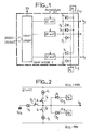
- FIGS 1, 2 and 3 of this application relate to the operation of the circuit described in patent application No. 2,515,402 to which reference will be made for more details.
- a plasma panel has two arrays of orthogonal electrodes, which are designated by the terms electrodes in x and electrodes in y.
- the control signals from the panel - maintenance, registration and erasure signals - are applied between two electrodes belonging to each of the networks.
- control circuit of patent application No. 2,515,402 consists of integrated circuits and amplifiers.
- the electrodes at x are controlled by integrated circuits which bear the reference X.
- Each integrated circuit X is associated with a single amplifier.
- the electrodes at y are controlled by integrated circuits which bear the reference Y.
- Each integrated circuit Y is associated with two amplifiers.
- This integrated circuit has three parts: a logic circuit, a low voltage / high voltage interface circuit, and an array of diodes.
- the logic circuit receives orders in low voltage logic defining the signal to be executed, its duration and the electrodes of the panel to be addressed. This logic circuit is supplied by a direct voltage of 12 V for example.
- the low voltage / high voltage interface circuit BT / HT in FIG. 1, is controlled by the logic circuit and makes it possible, during the preparation of the recording and erasing signals, to carry each electrode of the panel to a given voltage.
- This circuit is supplied with high voltage by sources of direct voltage external to the integrated circuit which supply voltages of values V CC2 ' V CC3' and V CC4 ' equal for example to + 100 V, - 100 V and 0 V.
- Each output of an interface circuit is connected to two diodes D 1 and D 2 mounted head to tail.
- Diode D 1 has its cathode connected to an output of the interface circuit and its anode connected to an E + y connection
- Diode D 2 has its anode connected to an output of the interface circuit and its cathode connected to an E -y connection
- FIG. 2 the constitution of a low voltage / high voltage interface circuit has been shown schematically in the case of the integrated circuit Y of FIG. 1.
- Each interface circuit comprises three switches I 1 , I 2 , I 3 , which are controlled by signals a, b and c supplied by the logic circuit and which are connected between an electrode of the connection panel V y and one of the three DC voltages V CC2 , V CC3 and V CC4 .
- Each of these switches is connected in series with a current source C 1 , C 2 and C 3 .
- FIG. 3 gives an exemplary embodiment of the diagram in FIG. 2.
- the switches I 1 and I 2 and the current sources C 1 and C 2 are constituted by two MOS transistors supporting a high voltage or DMOS, bearing the references T 1 , T 2 , T 3 , T 4 .
- Two resistors R and two zener diodes D 3 and D 4 are also required .
- Each DMOS therefore plays the role of a switch in series with a current source. For a given voltage applied to its gate, it transmits one of the voltages V CC2 , V CC3 to a connection V y and can supply a given drain-source current.
- two transistors T5 and T 6 are used controlled by signals c and c 'and two diodes D5 and D 6 .
- Two different types of transistors are required because during the preparation of the selective signals it is necessary to be able to supply or accept the current of each electrode.
- the diodes D5 and D 6 are there to compensate for the effect of the intrinsic diodes of the transistors T 5 and T 6 .
- each low voltage / high voltage interface circuit of an integrated circuit Y requires the use of 6 DMOS and that on the other hand the DMOS T 2 and T4 must be sized to support 200 V, that is -to say V CC2 -VCC3 'reverse voltage.
- the voltage to be supported is only 100 V, ie
- the low voltage / high voltage interface circuits of the integrated circuits Y have been modified.
- Integrated circuits X include, like integrated circuits Y, a logic circuit, a low voltage / high voltage interface circuit and an array of diodes.
- the low-voltage / high-voltage interface circuit of the integrated circuits X must, during the preparation of the recording and erasing signals, carry each electrode of the panel only with two states and not three, a state at 0 V or V CC4 and a ramp from 0 to 100 V , from V CC4 to V CC3 . It should also be noted that no component has to withstand 200 V of reverse voltage.
- the present invention relates to a control circuit of an alternating type plasma panel which ensures the development of the maintenance, recording and erasing signals of the panel. These signals are applied between two electrodes belonging to two orthogonal electrode networks, a first electrode network being controlled by integrated circuits associated with a single amplifier and a second electrode network being controlled by integrated circuits associated with two amplifiers , these amplifiers being used for the development of the maintenance signals.
- Each integrated circuit notably comprises a low voltage / high voltage interface circuit, controlled by a logic circuit and comprising means making it possible in particular during the preparation of the recording and erasing signals, to bring each electrode of the panel to a given voltage, this interface circuit being followed by a network of diodes.
- the low voltage / high voltage interface circuits of the integrated circuits associated with the second network of electrodes are supplied with high voltage by the two amplifiers associated with each of these integrated circuits.
- one of the amplifi cateurs supplies the voltage to be applied to the selected electrodes to be entered or deleted while the other amplifier supplies the voltage to be applied to the non-selected electrodes.
- FIG. 4 is the block diagram according to the invention of a low voltage / high voltage interface circuit used in an integrated circuit Y.
- these interface circuits are supplied with high voltage by the two amplifiers A 1 and A 2 associated with each integrated circuit Y. These interface circuits therefore receive the voltages E + y and E -y supplied by these two amplifiers A 1 and A 2 .
- Two switches I 1 and 1 2 controlled by low voltage logic signals a and b make it possible to apply to each electrode in y - connection V y - either E -y when the switch Il is closed, or E + y when the switch I 2 is closed, for the preparation of the recording and erasing signals.
- These switches are connected in series with current sources CI and C 2 .
- the switches I 1 , I 2 are open, the maintenance signals are developed as in the cited patent application thanks to the diodes D 1 and D 2 connected between on the one hand V and on the other hand E -y and E.
- Figure 6a shows the signal V y applied to an electrode at y.
- FIGS. 6b and c show the voltages E + y and E -y obtained at the output of the two amplifiers connected to each integrated circuit Y and applied according to the invention to each low voltage / high voltage interface circuit.
- FIGS. 6d and e show the control signals a and b applied to the switches I 1 and 1 2 in FIG. 4.
- the maintenance signals in slots of extreme values V CC2 and VCC 3 'equal for example to + 100 V and - 100 V and of intermediate value VCC 4 , equal by example at 0 V, are produced by two amplifiers supplying voltages E + y and E -y in slots identical to V y
- one of the amplifiers supplies the current necessary for the plasma panel during the rising edges of the maintenance signal and the other amplifier accepts current from the panel during the falling edges of the maintenance signal.
- the equality of the voltages E + y and E -y means that there is no current flow from E + y to E -y by the diodes.
- FIGS. 6b and c show in thick lines the portions of signals E and E -y which are applied to the electrodes at y and in thin lines, the portions of signals E + y and E -y which only serve to avoid the current flow between E and E, that is to say between the two amplifiers.
- the switches I 1 and 1 2 are open.
- the maintenance signals are developed in the same way as in the prior art where, according to the diagram in FIG. 2 of the present application, the switches I 1 , 1 2 and I 3 were open at that time.
- the switches I 1 , I 2 and I 3 are open and during the development of the recording and erasing signals , the voltages E + y and E -y at the output of the amplifiers must be such that they do not impose voltages on the low voltage / high voltage interface circuits which must deliver these signals.
- FIG. 6a the recording and erasing signals to be developed are shown.
- the dotted parts relate to the case where an electrode must be registered or deleted.
- the dashed parts relate to the opposite case, where the electrode must be kept in the same state.
- FIGS. 6b and c the voltages E + y and E -y which the amplifiers must supply are shown when the recording or erasing signals are produced so that the amplifiers do not impose any voltage on the electrodes in y.
- E + y and E -y are taken equal to V y except in the zones where V y can take two values. There, E takes the weakest of these values and E -y the strongest.
- the voltage E + y is equal to the voltage V y - in dotted lines - to be applied to the selected electrodes - to be entered or erased - and the voltage E -y is equal to the voltage V - in dashes - to be applied to the non-selected electrodes.
- the DC voltages of + 100 V, - 100 V in FIG. 2 are no longer used and the voltages E + y and E -y are used in each low-voltage / high-voltage interface circuit. develop the registration and erasure signals.
- the voltages E + y and E -y do not have to be modified. They will simply have to supply the energy necessary for the selective signals during their development while the amplifiers were passive in the prior art, during the development of the selective signals. Since the currents required for recording and erasing are much lower than those for maintenance, this will not require oversizing the amplifiers creating E + y and E.
- control signals a and b which control the switches Il and i 2 are identical for writing and erasing.
- the invention therefore makes it possible to simplify the logic circuits of the integrated circuits which supply a and b.
- the invention makes it possible to reduce the number of switches and current sources.
- FIG. 4 only two switches and two current sources are used whereas three are used in FIG. 3.
- All components can be dimensioned for a reverse voltage withstand of 100 V, that is to say of sup
- the invention therefore makes it possible to produce amplitude output signals (V CC4 , V CC2 ) and (V CC4 , V CC3 ) with components dimensioned for a reverse voltage of sup (
- signals of total amplitude 200 V are created from components supporting 100 V.
- FIG. 5 is an exemplary embodiment of the block diagram of FIG. 4.
- each switch has been made, associated with a current source, by two DMOS N 1 and P 1 for Il and N 2 and P 2 for I 2 .
- the transistor P1 of the P-type is connected between the output E -y of the amplifier A 2 and V y.
- the gate of P 1 is connected via a diode D5 to the N-type transistor N, the gate of which receives the control signal a and the source of which is connected to V CC4 , equal for example to 0 V.
- Diode D 5 is there to compensate for the effect of the intrinsic diode of transistor N 1 . Without the diode D 5, the intrinsic diode happen live when E -y is less than V CC4 and provo- q uence it a circulating current V CC4 to E -y
- the lower part of FIG. 5 has an arrangement similar to that of its upper part, with the transistors P2 and N 2 , the diodes D 4 and D6 and the resistor R, but the types of the transistors are reversed and the sign of the signal b is the opposite of that of a.
- diagram in FIG. 4 can be produced using another technology, in bipolar for example.
- the diodes D 1 and D 2 are in parallel on the intrinsic drain source diodes of the transistors P 1 and N 2 . We can remove the diodes D 1 and D 2 and reinforce the intrinsic diodes of P 1 and N 2 so that they can withstand the currents necessary for the maintenance signals. This also makes it possible to reduce the dimensions of the control circuit.
- the low voltage / high voltage interface circuits of FIGS. 4 and 5 are produced in the form of an integrated circuit Y also comprising a logic circuit and arrays of diodes as in the figure 1, it is necessary to ensure the polarization of the substrate of the integrated circuit.
- the voltages applied to this integrated circuit vary between - 100 V , V CC3 and + 100 V, V CC2 and the substrate of the integrated circuit must be at the most negative voltage of the circuit.
- V CC1 , V CC2 , V CC3 and V CC4 equal respectively to 12 V, + 100 V, - 100 V and 0 V. It is understood that these voltages can take different values.
Landscapes
- Engineering & Computer Science (AREA)
- Physics & Mathematics (AREA)
- Power Engineering (AREA)
- Plasma & Fusion (AREA)
- Computer Hardware Design (AREA)
- General Physics & Mathematics (AREA)
- Theoretical Computer Science (AREA)
- Control Of Indicators Other Than Cathode Ray Tubes (AREA)
Applications Claiming Priority (2)
| Application Number | Priority Date | Filing Date | Title |
|---|---|---|---|
| FR8315334 | 1983-09-27 | ||
| FR8315334A FR2552575B1 (fr) | 1983-09-27 | 1983-09-27 | Circuit de commande d'un panneau a plasma de type alternatif |
Publications (3)
| Publication Number | Publication Date |
|---|---|
| EP0150633A2 true EP0150633A2 (de) | 1985-08-07 |
| EP0150633A3 EP0150633A3 (en) | 1986-04-09 |
| EP0150633B1 EP0150633B1 (de) | 1988-08-17 |
Family
ID=9292572
Family Applications (1)
| Application Number | Title | Priority Date | Filing Date |
|---|---|---|---|
| EP84401893A Expired EP0150633B1 (de) | 1983-09-27 | 1984-09-21 | Ansteuersystem für eine Wechselstrom-Plasmaanzeigetafel |
Country Status (5)
| Country | Link |
|---|---|
| US (1) | US4652796A (de) |
| EP (1) | EP0150633B1 (de) |
| JP (1) | JPS6093485A (de) |
| DE (1) | DE3473523D1 (de) |
| FR (1) | FR2552575B1 (de) |
Cited By (1)
| Publication number | Priority date | Publication date | Assignee | Title |
|---|---|---|---|---|
| EP0351874A3 (en) * | 1988-07-22 | 1990-05-30 | Kabushiki Kaisha Toshiba | Output circuit |
Families Citing this family (9)
| Publication number | Priority date | Publication date | Assignee | Title |
|---|---|---|---|---|
| EP1231590A3 (de) * | 1991-12-20 | 2003-08-06 | Fujitsu Limited | Vorrichtung zur Steuerung einer Anzeigetafel |
| KR950003381B1 (ko) * | 1992-05-26 | 1995-04-12 | 삼성전관 주식회사 | 플라즈마 어드레스방식의 액정표시장치 및 그 구동방법 |
| JP2891280B2 (ja) * | 1993-12-10 | 1999-05-17 | 富士通株式会社 | 平面表示装置の駆動装置及び駆動方法 |
| US5623596A (en) | 1994-05-09 | 1997-04-22 | Apple Computer, Inc. | Power fault protection in a computer system having multiple power supplies |
| JP3364066B2 (ja) * | 1995-10-02 | 2003-01-08 | 富士通株式会社 | Ac型プラズマディスプレイ装置及びその駆動回路 |
| US6078205A (en) * | 1997-03-27 | 2000-06-20 | Hitachi, Ltd. | Circuit device, drive circuit, and display apparatus including these components |
| JP3642693B2 (ja) * | 1998-12-28 | 2005-04-27 | 富士通株式会社 | プラズマディスプレイパネル装置 |
| JP3201603B1 (ja) | 1999-06-30 | 2001-08-27 | 富士通株式会社 | 駆動装置、駆動方法およびプラズマディスプレイパネルの駆動回路 |
| KR100560490B1 (ko) * | 2003-10-16 | 2006-03-13 | 삼성에스디아이 주식회사 | 플라즈마 디스플레이 패널의 구동장치 및 구동방법 |
Family Cites Families (6)
| Publication number | Priority date | Publication date | Assignee | Title |
|---|---|---|---|---|
| US3851210A (en) * | 1973-06-22 | 1974-11-26 | Owens Illinois Inc | Method of driving and addressing gas discharge panels by inversion techniques |
| US3997813A (en) * | 1975-11-10 | 1976-12-14 | Burroughs Corporation | MOS integrated circuit chip for display panels |
| US4140945A (en) * | 1978-01-06 | 1979-02-20 | Owens-Illinois, Inc. | Sustainer wave form having enhancement pulse for increased brightness in a gas discharge device |
| JPS55136726A (en) * | 1979-04-11 | 1980-10-24 | Nec Corp | High voltage mos inverter and its drive method |
| JPS583264A (ja) * | 1981-06-30 | 1983-01-10 | Fujitsu Ltd | 高耐圧半導体集積回路およびその製造方法 |
| FR2515402B1 (de) * | 1981-10-23 | 1987-12-24 | Thomson Csf |
-
1983
- 1983-09-27 FR FR8315334A patent/FR2552575B1/fr not_active Expired
-
1984
- 1984-09-21 EP EP84401893A patent/EP0150633B1/de not_active Expired
- 1984-09-21 DE DE8484401893T patent/DE3473523D1/de not_active Expired
- 1984-09-24 US US06/653,919 patent/US4652796A/en not_active Expired - Fee Related
- 1984-09-25 JP JP59200338A patent/JPS6093485A/ja active Pending
Cited By (2)
| Publication number | Priority date | Publication date | Assignee | Title |
|---|---|---|---|---|
| EP0351874A3 (en) * | 1988-07-22 | 1990-05-30 | Kabushiki Kaisha Toshiba | Output circuit |
| US5113087A (en) * | 1988-07-22 | 1992-05-12 | Kabushiki Kaisha Toshiba | Output circuit |
Also Published As
| Publication number | Publication date |
|---|---|
| US4652796A (en) | 1987-03-24 |
| FR2552575B1 (fr) | 1985-11-08 |
| EP0150633B1 (de) | 1988-08-17 |
| EP0150633A3 (en) | 1986-04-09 |
| JPS6093485A (ja) | 1985-05-25 |
| FR2552575A1 (fr) | 1985-03-29 |
| DE3473523D1 (en) | 1988-09-22 |
Similar Documents
| Publication | Publication Date | Title |
|---|---|---|
| EP0150633B1 (de) | Ansteuersystem für eine Wechselstrom-Plasmaanzeigetafel | |
| EP2645569B1 (de) | Steuervorrichtung, die in einem Stromzuführungssystem mit Partitionierung verwendet wird | |
| FR2702317A1 (fr) | Circuit pompe de charge à faible consommation, faible bruit et synthétiseur de fréquence équipé d'un tel circuit. | |
| EP0194177B1 (de) | Teilnehmerschnittstellenschaltung mit Überwachungsbetrieb bei verringerter Speisung | |
| EP0670629A1 (de) | Phasenregelkreis | |
| FR3059498A1 (fr) | Procede et circuit de commande d'un dispositif de commutation d'un circuit de puissance | |
| FR2479605A1 (fr) | Disposition de circuit pour rendre symetrique le cycle d'hysteresis dans un feeder de type " push-pull " | |
| FR2767976A1 (fr) | Dispositif d'aide au demarrage pour une pluralite de sources de courant | |
| EP0538121B1 (de) | Anordnung zum Generieren einer Programmierspannung eines programmierbaren Festwertspeichers, insbesondere des EPROM-Typs, und dazugehörige Verfahren und Speicher | |
| FR2641388A1 (fr) | Circuit integre comprenant un generateur de courant commutable | |
| FR2461407A1 (fr) | Interrupteurs de courant alternatif utilisant des transistors a effet de champ | |
| EP0743586B1 (de) | Integrierte Schaltung in der einige Bauelemente mit dem selben Betriebsverhalten arbeiten sollen | |
| EP0281465A1 (de) | Speicherleseverstärker | |
| EP0763282B1 (de) | Schnittstelle zum umsetzen logischer ecl-pegel in cmos-pegel | |
| FR2477348A1 (fr) | Dispositif pour l'excitation d'un grand nombre d'electrodes image servant a l'enregistrement par voie non mecanique | |
| FR2821699A1 (fr) | Alternateur de vehicule automobile a sortie d'information d'excitation | |
| EP0221786A2 (de) | Anzeigetafel mit Leuchtdioden | |
| EP0164770B1 (de) | Statisches Relais für niedrige Gleichstromspannung | |
| FR2801148A1 (fr) | Commande analogique controlee | |
| FR2575013A1 (fr) | Porte logique a coincidence, et circuits logiques sequentiels mettant en oeuvre cette porte a coincidence | |
| FR2803400A1 (fr) | Dispositif de regulation | |
| WO2002011280A1 (fr) | Circuit electronique de conversion d'un signal et amplificateur integrant ledit circuit | |
| FR2777139A1 (fr) | Oscillateur a frequence controlee en courant, a reponse rapide | |
| EP3696981A1 (de) | Zelle eines statischen sicherheitsrelais und gesamtheit von zellen eines solchen statischen relais | |
| EP0690575A1 (de) | Vorrichtung zur Aktivierung einer Vorspannungsquelle |
Legal Events
| Date | Code | Title | Description |
|---|---|---|---|
| PUAI | Public reference made under article 153(3) epc to a published international application that has entered the european phase |
Free format text: ORIGINAL CODE: 0009012 |
|
| AK | Designated contracting states |
Designated state(s): DE GB NL |
|
| PUAL | Search report despatched |
Free format text: ORIGINAL CODE: 0009013 |
|
| AK | Designated contracting states |
Kind code of ref document: A3 Designated state(s): DE GB NL |
|
| 17P | Request for examination filed |
Effective date: 19860417 |
|
| 17Q | First examination report despatched |
Effective date: 19871106 |
|
| GRAA | (expected) grant |
Free format text: ORIGINAL CODE: 0009210 |
|
| AK | Designated contracting states |
Kind code of ref document: B1 Designated state(s): DE GB NL |
|
| REF | Corresponds to: |
Ref document number: 3473523 Country of ref document: DE Date of ref document: 19880922 |
|
| GBT | Gb: translation of ep patent filed (gb section 77(6)(a)/1977) | ||
| RAP4 | Party data changed (patent owner data changed or rights of a patent transferred) |
Owner name: THOMSON-CSF |
|
| PLBE | No opposition filed within time limit |
Free format text: ORIGINAL CODE: 0009261 |
|
| STAA | Information on the status of an ep patent application or granted ep patent |
Free format text: STATUS: NO OPPOSITION FILED WITHIN TIME LIMIT |
|
| 26N | No opposition filed | ||
| PGFP | Annual fee paid to national office [announced via postgrant information from national office to epo] |
Ref country code: DE Payment date: 19890810 Year of fee payment: 6 |
|
| PGFP | Annual fee paid to national office [announced via postgrant information from national office to epo] |
Ref country code: GB Payment date: 19890831 Year of fee payment: 6 |
|
| PGFP | Annual fee paid to national office [announced via postgrant information from national office to epo] |
Ref country code: NL Payment date: 19890930 Year of fee payment: 6 |
|
| PG25 | Lapsed in a contracting state [announced via postgrant information from national office to epo] |
Ref country code: GB Effective date: 19900921 |
|
| PG25 | Lapsed in a contracting state [announced via postgrant information from national office to epo] |
Ref country code: NL Effective date: 19910401 |
|
| GBPC | Gb: european patent ceased through non-payment of renewal fee | ||
| NLV4 | Nl: lapsed or anulled due to non-payment of the annual fee | ||
| PG25 | Lapsed in a contracting state [announced via postgrant information from national office to epo] |
Ref country code: DE Effective date: 19910601 |