EP0150811B1 - Méthode et appareil pour enregistrer des signaux numériques - Google Patents
Méthode et appareil pour enregistrer des signaux numériques Download PDFInfo
- Publication number
- EP0150811B1 EP0150811B1 EP85100696A EP85100696A EP0150811B1 EP 0150811 B1 EP0150811 B1 EP 0150811B1 EP 85100696 A EP85100696 A EP 85100696A EP 85100696 A EP85100696 A EP 85100696A EP 0150811 B1 EP0150811 B1 EP 0150811B1
- Authority
- EP
- European Patent Office
- Prior art keywords
- error detection
- signal
- block
- address
- data
- Prior art date
- Legal status (The legal status is an assumption and is not a legal conclusion. Google has not performed a legal analysis and makes no representation as to the accuracy of the status listed.)
- Expired
Links
- 238000000034 method Methods 0.000 title claims description 14
- 238000001514 detection method Methods 0.000 claims description 71
- 238000006243 chemical reaction Methods 0.000 claims 2
- 238000003672 processing method Methods 0.000 claims 1
- 238000012545 processing Methods 0.000 description 14
- 238000010586 diagram Methods 0.000 description 8
- 239000011159 matrix material Substances 0.000 description 5
- 230000002159 abnormal effect Effects 0.000 description 3
- 230000005540 biological transmission Effects 0.000 description 2
- 208000011580 syndromic disease Diseases 0.000 description 2
- 230000003321 amplification Effects 0.000 description 1
- 238000007796 conventional method Methods 0.000 description 1
- 230000000694 effects Effects 0.000 description 1
- 230000014509 gene expression Effects 0.000 description 1
- 238000003199 nucleic acid amplification method Methods 0.000 description 1
- 238000013139 quantization Methods 0.000 description 1
- 238000005070 sampling Methods 0.000 description 1
- 238000000638 solvent extraction Methods 0.000 description 1
Images




Classifications
-
- G—PHYSICS
- G11—INFORMATION STORAGE
- G11B—INFORMATION STORAGE BASED ON RELATIVE MOVEMENT BETWEEN RECORD CARRIER AND TRANSDUCER
- G11B20/00—Signal processing not specific to the method of recording or reproducing; Circuits therefor
- G11B20/10—Digital recording or reproducing
- G11B20/18—Error detection or correction; Testing, e.g. of drop-outs
- G11B20/1806—Pulse code modulation systems for audio signals
- G11B20/1809—Pulse code modulation systems for audio signals by interleaving
Definitions
- the present invention relates to a method and apparatus for recording digital signals and, particularly, to a method and apparatus for arranging error detection/correction codes suitable for block address protection in recording information on a PCM recorder.
- PCM audio recorders in which an analog signal is converted into a digital signal and it is recorded on a recording medium such as a magnetic tape, provide significantly improved sound quality as compared with the conventional analog signal tape recorders.
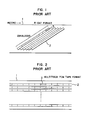
- the transmission rate is increased by about 50 times, and it is necessary to increase the transmission rate by increasing the number of recording tracks or increasing the relative tape speed with respect to the recording head through the use of a rotary head.
- another error detection code 7 is appended for the control signals 5 and block address 6, whereby the accuracy of reproducing the PCM signal can be enhanced.
- a brief error detection scheme as of the simple parity code can possibly encounter the misdetection of error.
- the probability of misdetection is as high as 1/2 8- 1, or 1/255.
- an error occurs in the block address 6, the order of data is disturbed, resulting in an improper deinterleaving of the PCM signal.
- Such improper deinterleaving causes the creation of abnormal sound such as a click noise in a digital audio reproducing system.
- an object of the present invention to provide a method and apparatus for arranging error detection/correction codes which effectively protect the block address of data recorded on a PCM recorder without increasing the redundancy of PCM data.
- Another object of the present invention is to provide a method of arranging error detection/ correction codes for a PCM audio system capable of preventing the creation of abnormal sound caused by incorrect deinterleaving of reproduced data even if the block address is reproduced erroneously.
- a PCM signal recording method is as defined in Claim 1.
- the following error detection/correction processings for the PCM signal can detect the disturbance, thereby preventing the disorderly data, namely, incorrectly deinterleaved data from being sent out of the system, or preventing an erroneous correction which would be caused by error correction using disorderly de-interleaved data.
- FIG. 5 shows a matrix for generating the error detection/correction codes 9 shown in Figure 3.
- the error detection/correction codes P o and P are determined from the block address 6 and PCM signal 8 so that the matrix of Figure 5 is satisfied.
- error syndromes So and S are calculated as follows.
- Figure 5 gives
- the P o and P 1 can be determined by calculating the above equations.
- the error detection/correction code generating block By making the error detection/correction code generating block to include the block address 6, even if the error detection code 7 has failed to detect an error due to an erroneous block address 6, the error can be detected by the following error detection using the error detection/correction codes 9.
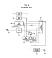
- FIG. 6 shows an example of the PCM signal recording system according to the present ihven- tion.
- the arrangement includes a synchronizing (sync) signal generator 11, a control signal generator 12, a random-access memory (RAM) 13 used for partitioning and interleaving the digital signal, a memory address controller 14, an error detection signal (P c ) generator 15, an error detection/correction code (P o , P,) generator 17, signal switching circuits 16 and 18 formed of multiplexers or the like, and a recording circuit 19 for providing a recording signal to a magnetic recording head.
- a synchronizing (sync) signal generator 11 a control signal generator 12
- RAM random-access memory
- P c error detection signal
- P o , P, error detection/correction code
- a PCM signal 8 entered through an input terminal 10 is stored in the RAM 13, and thereafter it is read out of the RAM 13 in the order of W o , W 1 ,...,W 15 for recording.
- An address controller 14 produces an address signal for making access to the RAM 13, and it also produces the block address 6 based on the RAM address for reading out the signal 8.
- the P c generator 15 produces an error detection code P c from a control signal 5 provided by the control signal generator 12 and a block address 6 provided by the address controller 14.
- the P 0 /P 1 generator 17 produces error detection/ correction codes P o and P 1 from the block address 6 andthe PCM signal 8 read out of the RAM 13.
- the switching circuit 18 selects the outputs of these signal generating circuits sequentially to form a complete block of data as shown in Figure 3.
- the signal switching circuit 18 selects the outputs of the sync signal generator 11, control signal generator 12, address controller 14 (block address), and the P c generator 15 sequentially, and delivers the data 4 through 7 in Figure 3 to the recording circuit 19.
- the signal switching circuit 16 selects the block address from the address controller 14, and it is entered to the P o / P 1 generator 17.
- the signal switching circuit 18 selects the output of the RAM 13 so that the PCM signal is read out in the order of W o , W 1 ,...,W 15 .
- the signal selection circuit 16 selects the output of the RAM 13, and the P 0 /P 1 generator 17 is also supplied with the same PCM signal.
- the circuit 17 produces the Po and P 1 upon receipt of the last word W 15 .
- the signal switching circuit 18 selects the output of the P 0 /P 1 generator 17 and delivers the P o and P 1 codes to the recording circuit 19.
- the PCM data interleaving method using RAM 13 and address controller 14 may be as disclosed in for example, T. Arai et al. "Digital Audio/Video Combination Recorder Using Custom Made LSI's, IC's", 69th AES Convention, No. 1791 (B-6), May 1981, and S. Ohashi et al., "An Effective Ram Accessing Method for TCM Processing Systems", 68th AES Convention, No. 1726 (D-4), March 1981.
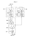
- Figure 7 shows in detail an example of the P 0 / P 1 generator 17.
- the arrangement includes an So generator 63, a S 1 generator 64, an arithmetic and logic (ALU) circuit 65, mod-2 adders 66A, 66B and 66C each formed of an EX-OR gate, latch circuits 67A and 67B, scale multipliers 68A and 68B performing multiplication between the input value and the values of a and 1/(1 +a), respectively, and a signal switching circuit 69.
- ALU arithmetic and logic
- An input data entered through an input terminal 61 is fed to the So generator 63 and S, generator 64, and after the addition operation by the respective adders 66A and 66B the results are held in the latch circuit 67A and 67B.
- error syndromes So and S are calculated in accordance with the expressions shown previously.
- the ALU circuit 65 performs computation for obtaining the value of P o or P, from the So and S,.
- the circuit 65 calculates the P o when the signal switching circuit 69 selects an input A, or calculates the P, when an input B is selected.
- the recording signal arranged in a block as shown in Figure 3 is further processed for modulation and the like by the recording circuit 19, and then recorded on the magnetic tape by the recording head 20.
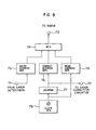
- Figure 8 shows an example of PCM signal reproducing system used to reproduce PCM signals that have been recorded as described above.
- the arrangement includes a playback head 22, a playback demodulator 23, a sync signal detector 24, an error detection circuit 26, an error flag register (RAM) 127, an error correction circuit 28, and a signal processing circuit 29.
- the digital signal picked up by the playback head 22 is processed for amplification and demodulation by the playback demodulator 23, and then fed through a bus 25 to the error detection circuit 26, error detection circuit 24 and de-interleaving RAM 113.
- the sync signal detector operates to detect the sync signal 4 which provides the reference timing for the successive reproducing operation.
- the error detection circuit 26 receives the control signal 5, block address 6 and error detection code 7 and performs error detection based on the error detection code 7. If the circuit 26 detects no error, the control signal 5 is sent to the signal processing circuit 29, and the block address 6 is sent to the address control circuit 114.
- the address control circuit 114 specifies the address of the RAM 113 for holding the PCM signal 8 and error detection/correction code 9 in accordance with the block address.
- the PCM signal 8 and error detection/correction codes 9 held in the memory 113 are thereafter read out into the error detection/correction circuit 28.
- the block addresses is produced from the address of memory 113, and it is fed to the error detection/correction circuit 28. Error detection is carried out using the error detection/ correction codes 9, and if an error is detected and it is found correctable, error correction is carried out successively. If the error is found uncorrected, an error detection flag 27 is set to the flag memory 127 from circuit 28.
- the PCM signal 8 is sent from the RAM 113 to the signal processing circuit 29, in which the signal is subjected to error concealment using the error detection flag 27 and processing by the control signal 5, and then the finished signal is delivered to an output terminal 30.
- the signal processing circuit 29 performs the second error correcting processing (C 2 decoding) using the second error detection/correction codes and the error detection flag.
- a presumed block address is produced based on the previously reproduced block address. If the presumed block address is erroneous, or if a block address including an undetected error is given to the address control circuit 114, the PCM data will be held at an erroneous location of the RAM 113, resulting in the reproduction of disorderly signal i.e., incorrectly deinterleaved data. In actual, however, the error detection/correction codes 9 are generated inclusive of the block address 6, and an erroneous block address can be detected in the error detecting processing by the error detection/ correction circuit 28.
- the error detection capability is enhanced significantly as evaluated to be 1/255x1/255 2 .
- Data held at an erroneous location of the RAM 113 is appended with an error detection flag, whereby disorderly data can be prevented from being sent out without correction, or miscorrection due to the second correcting process for disorderly data can be prevented.
- the capability of error detection and error correction can be enhanced through the use of the second error detection/ correction codes Q o -Q 3 in addition to the first error codes P o and P, and through the interleaving thereof.
- the second code block will erroneously include data of another code block, resulting much possibly in miscorrection in the second error correction.
- the present method uses the error detection flag appended to data of different code block, allowing the detection of that data in the second correction processing, whereby miscorrection can be prevented.
Landscapes
- Engineering & Computer Science (AREA)
- Multimedia (AREA)
- Signal Processing (AREA)
- Signal Processing For Digital Recording And Reproducing (AREA)
Claims (6)
Applications Claiming Priority (2)
| Application Number | Priority Date | Filing Date | Title |
|---|---|---|---|
| JP10098/84 | 1984-01-25 | ||
| JP59010098A JPH0770177B2 (ja) | 1984-01-25 | 1984-01-25 | ディジタル信号再生装置 |
Publications (3)
| Publication Number | Publication Date |
|---|---|
| EP0150811A2 EP0150811A2 (fr) | 1985-08-07 |
| EP0150811A3 EP0150811A3 (en) | 1987-08-05 |
| EP0150811B1 true EP0150811B1 (fr) | 1990-12-12 |
Family
ID=11740843
Family Applications (1)
| Application Number | Title | Priority Date | Filing Date |
|---|---|---|---|
| EP85100696A Expired EP0150811B1 (fr) | 1984-01-25 | 1985-01-24 | Méthode et appareil pour enregistrer des signaux numériques |
Country Status (4)
| Country | Link |
|---|---|
| US (1) | US4682332A (fr) |
| EP (1) | EP0150811B1 (fr) |
| JP (1) | JPH0770177B2 (fr) |
| DE (1) | DE3580852D1 (fr) |
Families Citing this family (62)
| Publication number | Priority date | Publication date | Assignee | Title |
|---|---|---|---|---|
| DE3650476T2 (de) * | 1985-10-11 | 1996-05-30 | Mitsubishi Electric Corp | PCM-Aufzeichnungs- und Wiedergabegerät |
| US4796110A (en) * | 1986-02-18 | 1989-01-03 | Irwin Magnetic Systems, Inc. | System and method for encoding and storing digital information on magnetic tape |
| JPS6356022A (ja) * | 1986-08-26 | 1988-03-10 | Victor Co Of Japan Ltd | デイジタル記録再生装置 |
| JPS63108566A (ja) * | 1986-10-27 | 1988-05-13 | Victor Co Of Japan Ltd | デイジタルミユ−テイング回路 |
| JP2526875B2 (ja) * | 1986-11-05 | 1996-08-21 | ソニー株式会社 | デイジタル情報記録装置 |
| EP0276991B1 (fr) * | 1987-01-30 | 1992-05-13 | Sony Corporation | Procédé et appareil de codage pour enregistrer des données avec un code d'identification et un code pour contrôler les erreurs |
| AU606125B2 (en) * | 1987-02-06 | 1991-01-31 | Sony Corporation | Apparatus for reproducing a digital signal |
| DE3719404A1 (de) * | 1987-06-11 | 1988-12-22 | Bosch Gmbh Robert | Verfahren und anordnung zur korrektur von fehlern in digitalen signalen |
| JPH0193933A (ja) * | 1987-10-06 | 1989-04-12 | Sony Corp | エラー訂正符号化装置 |
| US5172380A (en) * | 1988-06-30 | 1992-12-15 | Sony Corporation | Digital signal transmission apparatus |
| JPH0213135A (ja) * | 1988-06-30 | 1990-01-17 | Sony Corp | ディジタル信号伝送装置 |
| JPH02192077A (ja) * | 1989-01-19 | 1990-07-27 | Sharp Corp | データ記録/再生装置 |
| US5099484A (en) * | 1989-06-09 | 1992-03-24 | Digital Equipment Corporation | Multiple bit error detection and correction system employing a modified Reed-Solomon code incorporating address parity and catastrophic failure detection |
| JPH05174496A (ja) * | 1991-12-25 | 1993-07-13 | Sony Corp | ディジタル記録装置のid信号処理装置 |
| US5448420A (en) * | 1993-08-02 | 1995-09-05 | Dictaphone Corporation | Method and a system for storing audio |
| US5615222A (en) * | 1994-02-04 | 1997-03-25 | Pacific Communication Sciences, Inc. | ADPCM coding and decoding techniques for personal communication systems |
| US6580683B1 (en) | 1999-06-23 | 2003-06-17 | Dataplay, Inc. | Optical recording medium having a master data area and a writeable data area |
| US6898164B2 (en) | 2001-01-25 | 2005-05-24 | Dphi Acquisitions, Inc. | Close tracking algorithm in a digital tracking servo system |
| US6813228B2 (en) | 2001-01-25 | 2004-11-02 | Dphi Acquisitions, Inc. | Tracking and focus servo system with direction sensor |
| US6738320B2 (en) | 2001-01-25 | 2004-05-18 | Dphi Acquisitions, Inc. | System and method for moving optical pick up from current position to target position with smooth control |
| US7260031B2 (en) | 2001-01-25 | 2007-08-21 | Dphi Acquisitions, Inc. | Digital focus and tracking servo system with one-track jump |
| US6781929B2 (en) | 2001-01-25 | 2004-08-24 | Dphi Acquisitions, Inc. | Digital tracking servo system with multi-track seek |
| US6958957B2 (en) * | 2001-01-25 | 2005-10-25 | Dphi Acquisitions, Inc. | Digital tracking and focus servo system with TES to FES crosstalk calibration |
| US7092322B2 (en) * | 2001-01-25 | 2006-08-15 | Dphi Acquisitions, Inc. | Calibration of focus error signal offset in a focus servo system |
| US7680004B2 (en) * | 2001-01-25 | 2010-03-16 | Dphi Acquisitions, Inc. | Digital servo system with inverse non-linearity compensation |
| US6813226B2 (en) | 2001-01-25 | 2004-11-02 | Dphi Acquisitions, Inc. | Calibration of a focus sum threshold in a focus servo system |
| US6950380B2 (en) * | 2001-01-25 | 2005-09-27 | Dphi Acquisitions, Inc. | Detector input dark current offset calibration in an optical disk drive digital servo |
| US6891781B2 (en) * | 2001-01-25 | 2005-05-10 | Dphi Acquisitions, Inc. | Digital servo system with second order compensator |
| US7672199B2 (en) | 2001-01-25 | 2010-03-02 | Dphi Acquisitions, Inc. | Close focus algorithm in a digital focus servo system |
| US6937543B2 (en) | 2001-01-25 | 2005-08-30 | Dphi Acquisitions, Inc. | Digital focus servo system with a sliding notch filter |
| US6970403B2 (en) * | 2001-01-25 | 2005-11-29 | Dphi Acquisition, Inc. | Calibration of tracking error signal offset in a tracking servo system |
| US7023766B2 (en) | 2001-01-25 | 2006-04-04 | Dphi Acquisitions, Inc. | Flexible servicing of servo algorithms using a digital signal processor |
| US7095683B2 (en) * | 2001-01-25 | 2006-08-22 | Dphi Acquisitions, Inc. | Tracking and focus digital servo system with write abort |
| US6970410B2 (en) * | 2001-01-25 | 2005-11-29 | Dphi Acquisitions, Inc. | Focus detection in a digital focus servo system |
| US6891789B2 (en) * | 2001-01-25 | 2005-05-10 | Dphi Acquisitions, Inc. | Tracking and focus servo system with automatic media type detector |
| US6909676B2 (en) * | 2001-01-25 | 2005-06-21 | Dphi Acquisitions, Inc. | Digital tracking servo system with multi-track seek with track zero crossing detection |
| US6847597B2 (en) | 2001-01-25 | 2005-01-25 | Dphi Acquisitions, Inc. | Optical disk drive with a digital focus and tracking servo system |
| US6965547B2 (en) * | 2001-01-25 | 2005-11-15 | Dphi Acquisitions, Inc. | Tracking and focus servo system with error signal inverse non-linearity calibration |
| US7522480B2 (en) | 2001-01-25 | 2009-04-21 | Dphi Acquisitions, Inc. | Digital tracking servo system with multi-track seek with an acceleration clamp |
| US7196979B2 (en) | 2001-01-25 | 2007-03-27 | Dphi Acquisitions, Inc. | Calibration storage methods for a digital focus and tracking servo system with calibration |
| US7414940B2 (en) | 2001-01-25 | 2008-08-19 | Dphi Acquisitions, Inc. | Calibration of a focus error signal gain in a focus servo system |
| US6906985B2 (en) | 2001-01-25 | 2005-06-14 | Dphi Acquisitions, Inc. | Calibration of tracking error signal gain in a tracking servo system |
| US7023776B2 (en) * | 2001-01-25 | 2006-04-04 | Dphi Acquisitions, Inc. | Calibration initiation methods for a tracking and focus servo system |
| US6930963B2 (en) | 2001-01-25 | 2005-08-16 | Dphi Acquistions, Inc. | Tracking and focus servo system with head load |
| US6728182B2 (en) | 2001-01-25 | 2004-04-27 | Dphi Acquisitions, Inc. | Tracking and focus servo system with a media type boundary crossing detector |
| US6809995B2 (en) | 2001-01-25 | 2004-10-26 | Dphi Acquisitions, Inc. | Digital focus and tracking servo system |
| US6904007B2 (en) * | 2001-01-25 | 2005-06-07 | Dphi Acquisitions, Inc. | Digital servo system with loop gain calibration |
| US6704261B2 (en) | 2001-01-25 | 2004-03-09 | Dphi Acquisitions, Inc. | Spin motor control in an optical drive |
| US6922380B2 (en) | 2001-01-25 | 2005-07-26 | Dphi Acquisitions, Inc. | Tracking and focus servo system with anti-skate algorithm |
| US6762980B2 (en) | 2001-01-25 | 2004-07-13 | Dphi Acquisitions, Inc. | Digital tracking servo system with a multi-track seeking and accelerated servo function for regaining a closed tracking loop |
| US6882603B2 (en) * | 2001-01-25 | 2005-04-19 | Dphi Acquisitions, Inc. | Digital tracking servo system with tracking skate detection |
| US7492675B2 (en) * | 2001-01-25 | 2009-02-17 | Dphi Acquisitions, Inc. | Digital servo system with calibrated notch filters |
| US6956797B2 (en) * | 2001-01-25 | 2005-10-18 | Dphi Acquisitions, Inc. | Digital servo system with error signal integrity testing |
| US7016280B2 (en) * | 2001-01-25 | 2006-03-21 | Dphi Acquisitions, Inc. | Tracking and focus servo system with defect detection |
| US7782721B2 (en) * | 2001-01-25 | 2010-08-24 | Dphi Acquisitions, Inc. | Digital focus and tracking servo system with multi-zone calibration |
| US6847596B2 (en) | 2001-01-25 | 2005-01-25 | Dphi Acquisitions, Inc. | Tracking servo system including a multi-track seek algorithm with a track zero crossing period integrity test |
| US7593300B2 (en) | 2001-01-25 | 2009-09-22 | Dphi Acquisitions, Inc. | Digital tracking servo system with off-format detection |
| US6885619B2 (en) * | 2001-01-25 | 2005-04-26 | Dphi Acquisitions, Inc. | Detector input stray light offset calibration in an optical disk drive |
| US7020054B2 (en) * | 2001-01-25 | 2006-03-28 | Dphi Acquisitions, Inc. | Digital servo system with biased feed-forward |
| US6882601B2 (en) | 2001-01-25 | 2005-04-19 | Dphi Acquisitions, Inc. | Digital servo system with feed-forward control loops |
| US7228490B2 (en) * | 2004-02-19 | 2007-06-05 | Quantum Corporation | Error correction decoder using cells with partial syndrome generation |
| US8479079B2 (en) * | 2010-04-09 | 2013-07-02 | International Business Machines Corporation | Integrated data and header protection for tape drives |
Family Cites Families (12)
| Publication number | Priority date | Publication date | Assignee | Title |
|---|---|---|---|---|
| US3753228A (en) * | 1971-12-29 | 1973-08-14 | Westinghouse Air Brake Co | Synchronizing arrangement for digital data transmission systems |
| US4208650A (en) * | 1978-01-30 | 1980-06-17 | Forney Engineering Company | Data transmission system |
| US4282551A (en) * | 1979-04-11 | 1981-08-04 | Hitachi, Ltd. | PCM Recording and reproducing apparatus |
| JPS5665309A (en) * | 1979-10-26 | 1981-06-03 | Sony Corp | Time-axis converter |
| JPS5724005A (en) * | 1980-07-17 | 1982-02-08 | Sony Corp | Digital signal processor |
| JPS5792411A (en) * | 1980-11-28 | 1982-06-09 | Sony Corp | Pcm signal processor |
| JPS5794911A (en) * | 1980-12-01 | 1982-06-12 | Sony Corp | Pcm signal processor |
| GB2095440B (en) * | 1981-03-23 | 1985-10-09 | Sony Corp | Digital television signal processing |
| JPS5819712A (ja) * | 1981-07-29 | 1983-02-04 | Hitachi Ltd | デ−タ記録方式 |
| JPS58198935A (ja) * | 1982-05-15 | 1983-11-19 | Sony Corp | デ−タ伝送方法 |
| JPS5922208A (ja) * | 1982-07-06 | 1984-02-04 | Victor Co Of Japan Ltd | デイジタル情報信号記録方式 |
| GB2124806B (en) * | 1982-08-06 | 1986-05-14 | Sony Corp | Method of correcting errors in binary data |
-
1984
- 1984-01-25 JP JP59010098A patent/JPH0770177B2/ja not_active Expired - Lifetime
-
1985
- 1985-01-24 US US06/694,658 patent/US4682332A/en not_active Expired - Lifetime
- 1985-01-24 EP EP85100696A patent/EP0150811B1/fr not_active Expired
- 1985-01-24 DE DE8585100696T patent/DE3580852D1/de not_active Expired - Lifetime
Also Published As
| Publication number | Publication date |
|---|---|
| JPS615477A (ja) | 1986-01-11 |
| JPH0770177B2 (ja) | 1995-07-31 |
| DE3580852D1 (de) | 1991-01-24 |
| US4682332A (en) | 1987-07-21 |
| EP0150811A2 (fr) | 1985-08-07 |
| EP0150811A3 (en) | 1987-08-05 |
Similar Documents
| Publication | Publication Date | Title |
|---|---|---|
| EP0150811B1 (fr) | Méthode et appareil pour enregistrer des signaux numériques | |
| US4881232A (en) | Method and apparatus for error correction | |
| US4546474A (en) | Method of error correction | |
| US4447902A (en) | Error-correction format for digital television signals | |
| US4497058A (en) | Method of error correction | |
| EP0129849A2 (fr) | Procédé et système pour corriger des erreurs | |
| EP0232133B1 (fr) | Correction d'erreur de signaux numériques | |
| EP0048933B1 (fr) | Circuit pour corriger les erreurs dans un signal d'information numérique | |
| EP0317197B1 (fr) | Méthode de détection et de correction d'erreur | |
| US5805469A (en) | Digital audio signal processing apparatus and method for error concealment | |
| EP0334580B1 (fr) | Système et méthode pour la réalisation de correction d'erreurs de signaux audio, sur bande à format de trame fixe vidéo | |
| EP0146637B1 (fr) | Procede de detection d'erreur | |
| US6598197B1 (en) | Method and apparatus for detecting and concealing data errors in stored digital data | |
| EP0341863B1 (fr) | Méthode de détection de la synchronisation erronée d'un secteur | |
| US4491882A (en) | Disc players | |
| JP2574740B2 (ja) | Pcm信号再生装置 | |
| EP0411835B1 (fr) | Dispositif de décodage | |
| US4727547A (en) | Method and apparatus for decoding | |
| JPH07109697B2 (ja) | エラー訂正符号化装置 | |
| JPH02182034A (ja) | データ語におけるエラーを検出して補正する方法および回路装置 | |
| JP2000010807A (ja) | ディジタルデータ再生装置 | |
| JP2664267B2 (ja) | 符号誤り訂正装置 | |
| JP3282425B2 (ja) | ディジタル信号記録装置 | |
| JPS6117060B2 (fr) | ||
| JPS6314428B2 (fr) |
Legal Events
| Date | Code | Title | Description |
|---|---|---|---|
| PUAI | Public reference made under article 153(3) epc to a published international application that has entered the european phase |
Free format text: ORIGINAL CODE: 0009012 |
|
| 17P | Request for examination filed |
Effective date: 19850124 |
|
| AK | Designated contracting states |
Designated state(s): DE FR GB IT NL |
|
| PUAL | Search report despatched |
Free format text: ORIGINAL CODE: 0009013 |
|
| AK | Designated contracting states |
Kind code of ref document: A3 Designated state(s): DE FR GB IT NL |
|
| 17Q | First examination report despatched |
Effective date: 19890720 |
|
| GRAA | (expected) grant |
Free format text: ORIGINAL CODE: 0009210 |
|
| AK | Designated contracting states |
Kind code of ref document: B1 Designated state(s): DE FR GB NL |
|
| REF | Corresponds to: |
Ref document number: 3580852 Country of ref document: DE Date of ref document: 19910124 |
|
| ET | Fr: translation filed | ||
| PLBE | No opposition filed within time limit |
Free format text: ORIGINAL CODE: 0009261 |
|
| STAA | Information on the status of an ep patent application or granted ep patent |
Free format text: STATUS: NO OPPOSITION FILED WITHIN TIME LIMIT |
|
| 26N | No opposition filed | ||
| PGFP | Annual fee paid to national office [announced via postgrant information from national office to epo] |
Ref country code: NL Payment date: 19940131 Year of fee payment: 10 |
|
| PG25 | Lapsed in a contracting state [announced via postgrant information from national office to epo] |
Ref country code: NL Effective date: 19950801 |
|
| NLV4 | Nl: lapsed or anulled due to non-payment of the annual fee |
Effective date: 19950801 |
|
| REG | Reference to a national code |
Ref country code: GB Ref legal event code: IF02 |
|
| PGFP | Annual fee paid to national office [announced via postgrant information from national office to epo] |
Ref country code: FR Payment date: 20031219 Year of fee payment: 20 |
|
| PGFP | Annual fee paid to national office [announced via postgrant information from national office to epo] |
Ref country code: GB Payment date: 20031229 Year of fee payment: 20 |
|
| PGFP | Annual fee paid to national office [announced via postgrant information from national office to epo] |
Ref country code: DE Payment date: 20040304 Year of fee payment: 20 |
|
| PG25 | Lapsed in a contracting state [announced via postgrant information from national office to epo] |
Ref country code: GB Free format text: LAPSE BECAUSE OF EXPIRATION OF PROTECTION Effective date: 20050123 |
|
| REG | Reference to a national code |
Ref country code: GB Ref legal event code: PE20 |